Audio Codec Breakout - WM8960 Hookup Guide
 QCPete,
  bboyho
Hardware Overview
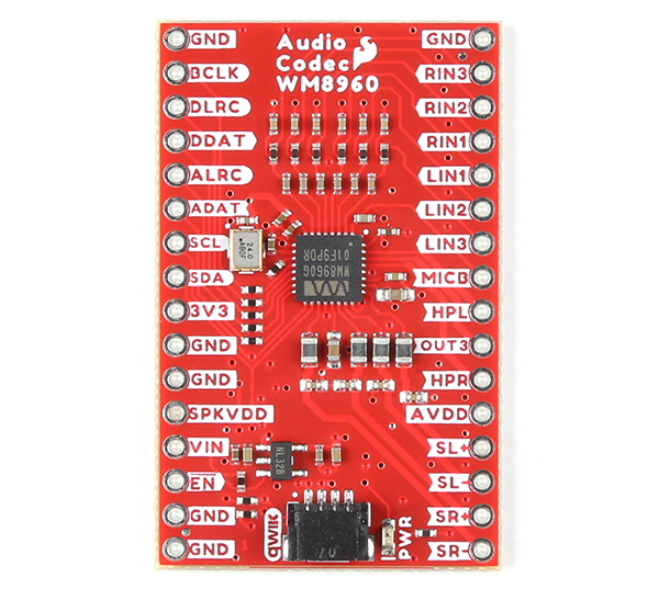
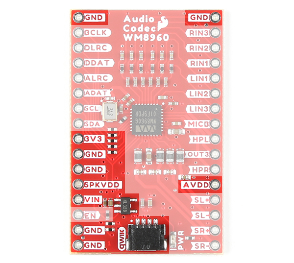
We broke out the pins of the WM8960 onto a breakout board to standard 0.1" spaced PTH. We'll highlight relevant application circuits, hardware, and pins that are broken out in this section.
 |
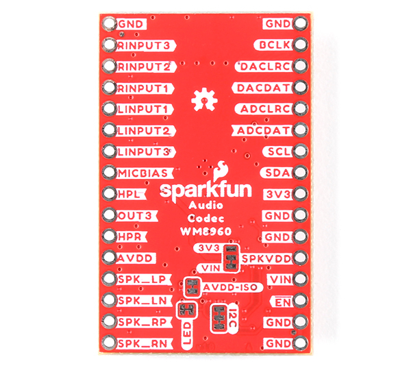 |
| Top View | Bottom View |
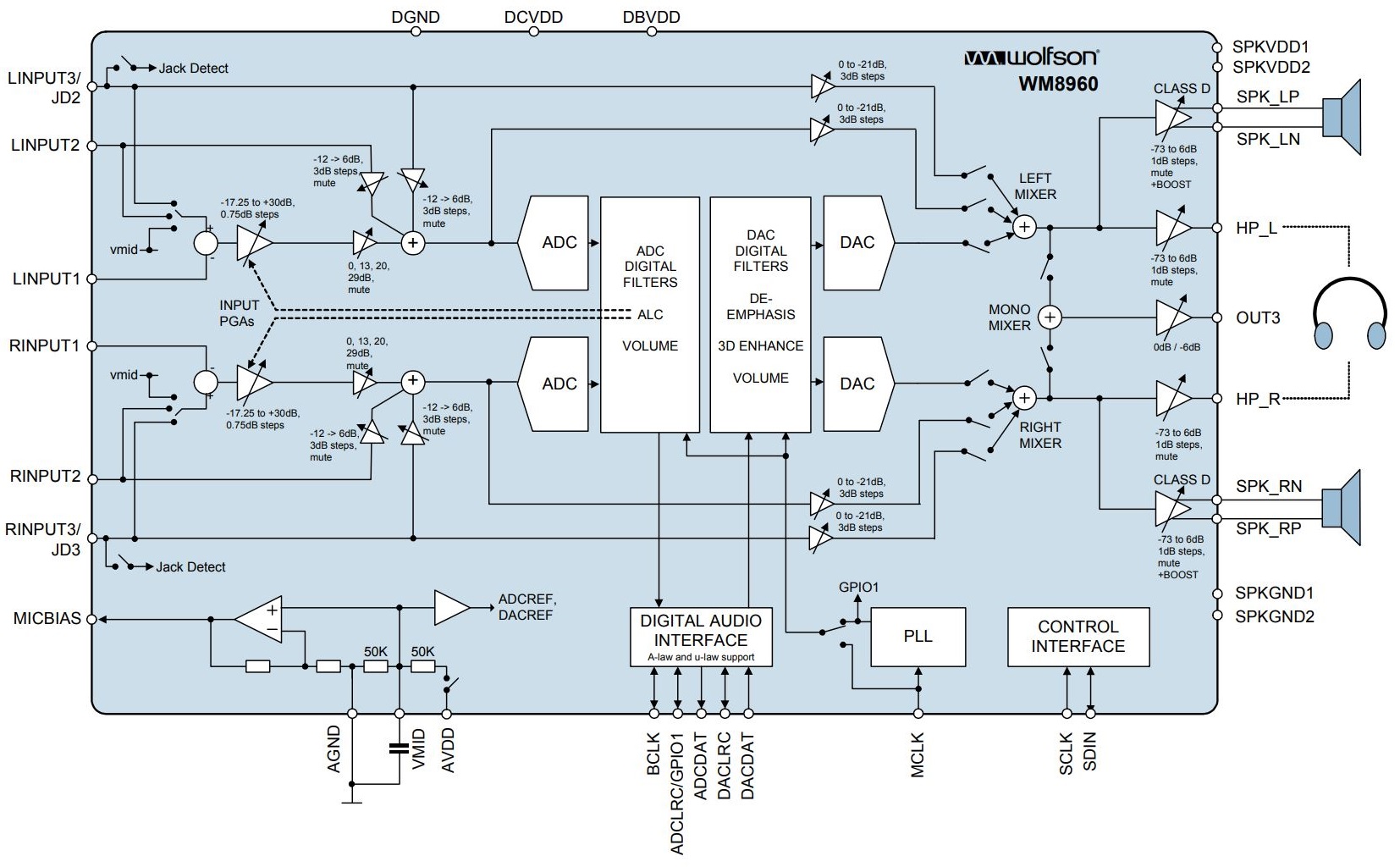
Keep in mind that the WM8960 is chock full of features as you can see from the datasheet's block diagram below. The input and output will depend on your project's needs. We recommend referencing the block diagrams listed in the datasheet to follow along. For more information, check out the datasheet linked in the Resources and Going Further.
Power
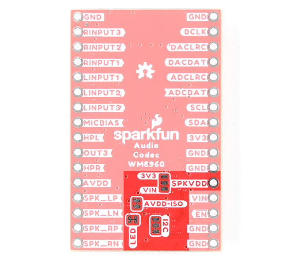
There are a variety of power and power-related nets broken out to the Qwiic connector and through hole pads on the edge of the board. The nets consist of the following.
- VIN - Voltage input for the analog and speaker circuits. The input voltage is between 3.7V and 5.5V.
- SPKVDD - By default, the VIN pin is connected directly to SPKVDD. The connection can be disabled but cutting the jumper on the back between VIN and SPKVDD. There is an option to connect the SPKVDD pad to the 3V3 pin by adding a solder blob between the two pads. If you decide to provide your own voltage, users will need to keep the jumpers open. The recommended voltage for this pin is between 2.7V and 5.5V.
- AVDD - Voltage from the VIN pin is regulated down to 3.3V from the XC6222 3.3V/700mA voltage regulator. This voltage is used to power the analog circuit. For users that want to provide their own voltage, cut the jumper on the back of the board labeled as AVDD-ISO. The recommended voltage for this pin is between 2.7V and 3.6V.
- 3V3 - This pin is broken out on the edge of the board as well as the Qwiic connector. This voltages is used to power the digital circuit. This voltage is tied to the IC's DCVDD and DBVDD pins. Note that this is on a separate net and not connected to the 3.3V voltage regulator. The recommended voltage for this pin is between 1.7V and 3.6V. This will typically be 3.3V when connecting to a microcontroller's 3.3V voltage regulator and Qwiic connector.
- GND - Common, ground voltage (0V reference) for the system.
To get started powering the audio codec, you will just need to provide power to the VIN and 3V3 pins. We recommend using your development board's voltages without adjusting the jumpers. For example, the IoT RedBoard - ESP32 Development Board can provide 5V through the female header and 3.3V through the Qwiic connector. Users can connect 5V to the audio codec's VIN pin to power the analog and speaker circuit. To power the digital circuit, users can provide 3.3V by adding a Qwiic cable between the Qwiic connectors. Of course, you will need to also connect your reference voltage for your system. By using the Qwiic cable, you will be connecting GND on both boards.
For users providing their own power supply for SPKVDD and AVDD, make sure to keep the jumpers open.
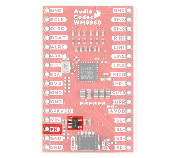
Enable Pin
The enable pin (labeled as EN) on the edge of the board is active low. Pulling the pin low will disable the 3.3V voltage regulator XC6222 that is connected to AVDD.
Digital Audio Interface
The board breaks out pins for the digital audio interface. This is used for inputting DAC data into the WM8960 and outputting ADC data from the IC.
- BCLK - Bit clock, for synchronization. This can be set as an input or output depending on the configuration.
- DLRC or DACLRC - DAC data left and right alignment clock. This can be set as an input or output depending on the configuration.
- DDAT or DACDAT - DAC data input.
- ALRC or ADCLRC - ADC data left and right alignment clock. This can be set as an input or output depending on the configuration.
- This pin can also be configured as a GPIO pin (e.g. GPIO1). As stated in the datasheet, the ADC will use the DACLRC as a frame clock for the ADCs and DACs. The ADCLRC/GPIO1 pin function should not be modified when the ADC is enabled. For more information check out the section about the Digital Audio Interface in the datasheet on pg 48.
- ADAT or ADCDAT - ADC data output.
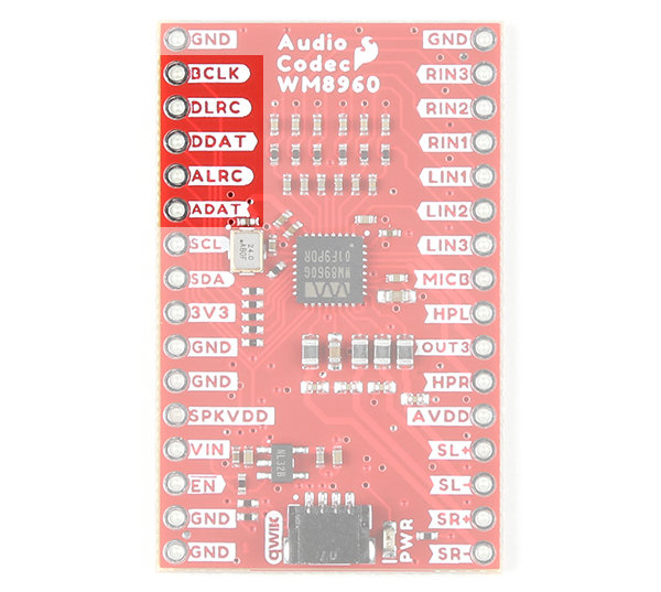
Four audio data formats listed below are supported.
- Left justified
- Right justified
- I2S (not to be confused with I2C)
- DSP
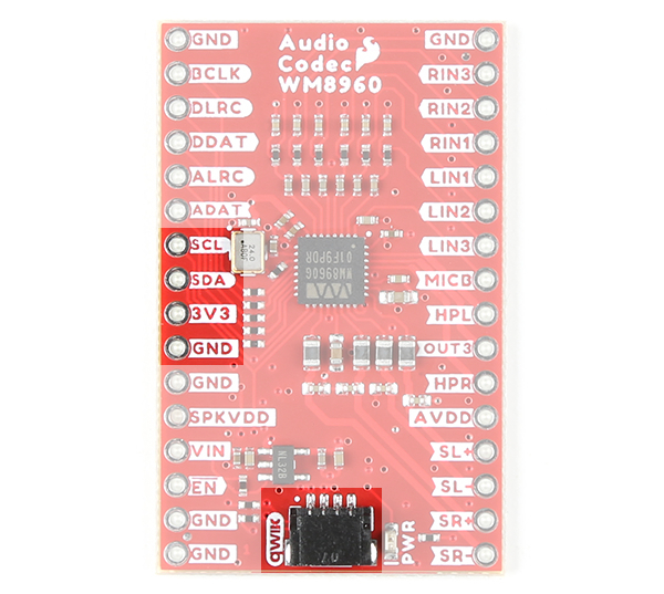
Qwiic and I2C
The board includes one Qwiic connector to configure the I2S settings and analog audio path. For users that need to solder directly to the board, the pins are also broken out on the edge PTH. The I2C data and clock lines are also tied to 2.2kΩ pull-up resistors. The default address of the WM8960 is 0x1A. Note that the datasheet shows the address as 0x34h, which is 0x1A shifted left 1 bit and then includes the appended "0" (aka write bit).
Stereo Input
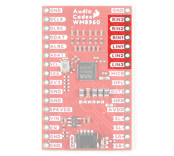
The WM8960 includes 6x flexible analog input pins. These pins can be used for line level or microphone level (balanced or un-balanced). Note that balanced microphones refers to differential microphones while un-balanced microphones refers to single-ended microphones.
- RIN3 / RINPUT3 - Right analog input 3 pin. This is connected to RINPUT3 or JD3.
- right channel, line input
- right channel, differential +MIC input
- jack detect input pin
- RIN2 / RINPUT2 - Right analog input 2 pin. This is connected to RINPUT2.
- right channel, line input
- right channel, differential +MIC input
- RIN1 / RINPUT1 - Right analog input 1 pin. This is connected to RINPUT1.
- right channel, single-ended MIC input
- right channel, differential -MIC input
- LIN1 / LINPUT1 - Left analog input 1 pin. This is connected to LINPUT1.
- left channel, single-ended MIC input
- left channel differential -MIC input
- LIN2 / LINPUT2 - Left analog input 2 pin. This is connected to LINPUT2.
- left channel, line input
- left channel, differential +MIC input
- LIN3 / LINPUT3 - Left analog input 3 pin. This is connected to LINPUT3 or JD2.
- left channel, line input
- left channel, differential +MIC input
- jack detect input pin
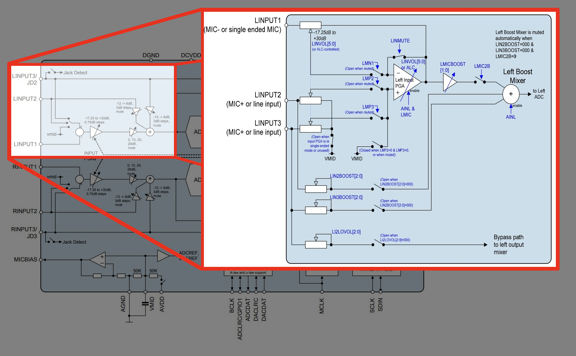
Remember the block diagram that was linked earlier just before soldering the headers to the board? The datasheet goes into more detail with the input path for the left and right channel.
Below is a modified image of the block diagram that highlights the input signal path before the left ADC for the left input channels on page 19.
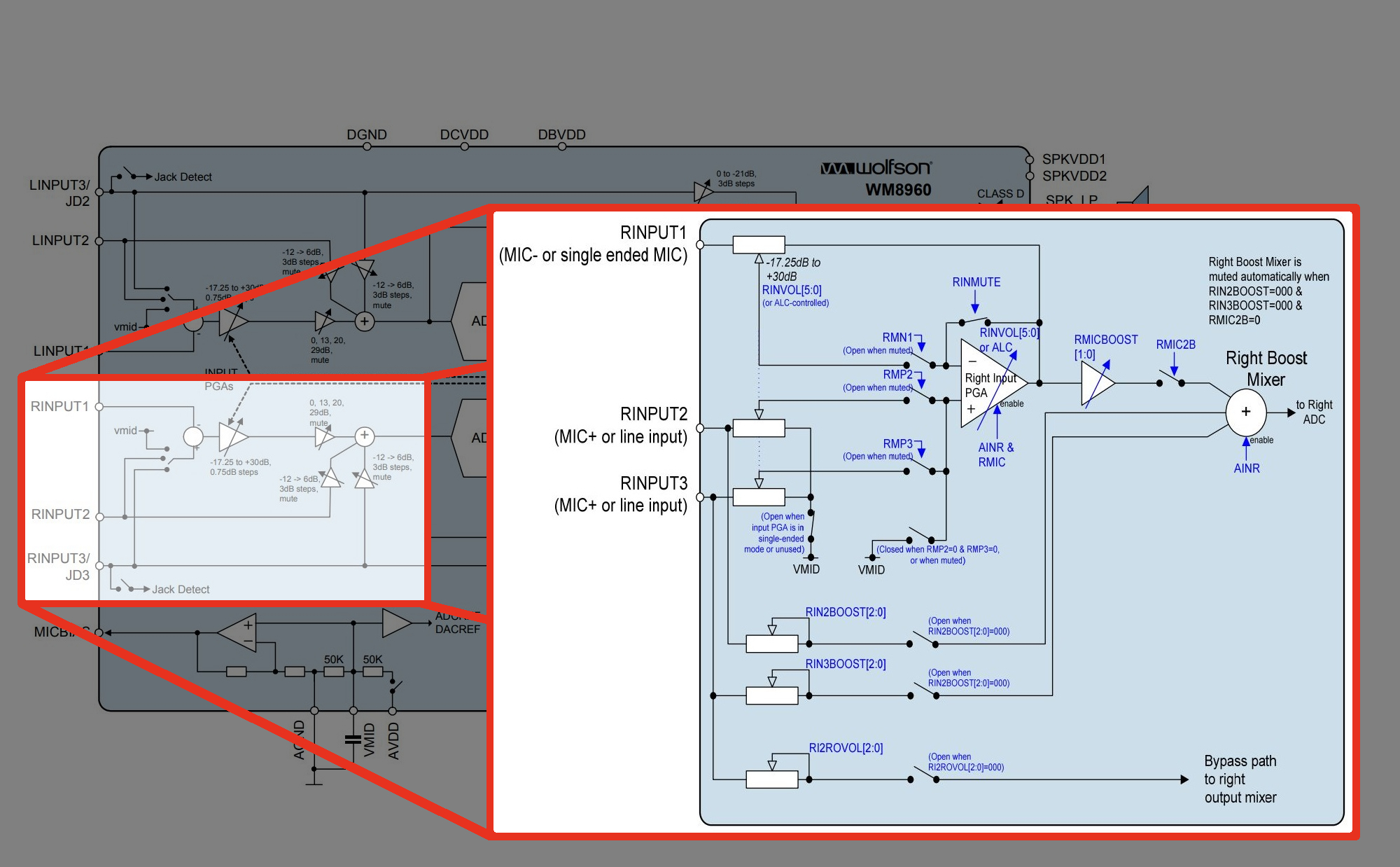
Below is a modified image of the block diagram that highlights the input signal path before the right ADC for the right input channels on page 20.
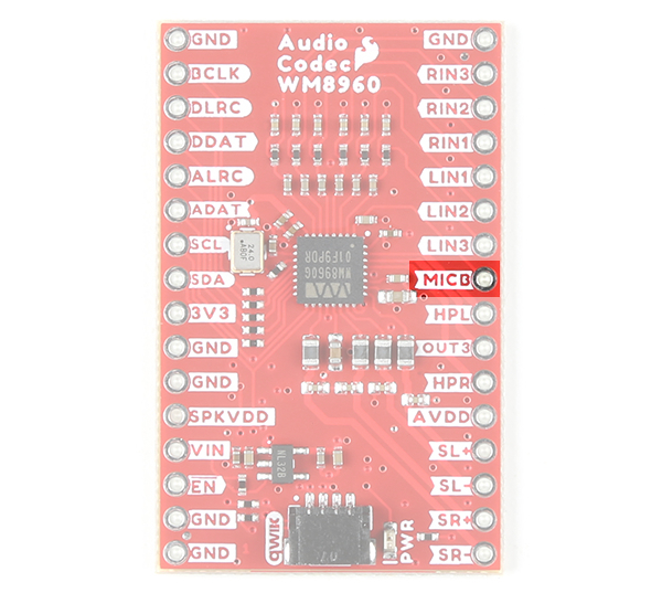
Microphone Bias
The MICB or MICBIAS provides a low noise reference voltage for biasing eletret condenser microphones (ECMs).
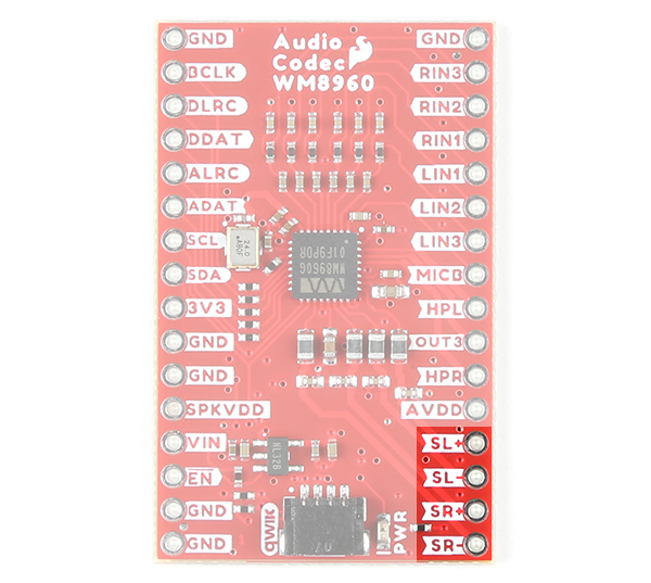
Speaker Out
The WM8960 includes differential stereo speaker outputs for the left and right speaker. The speaker is rated as a class D speaker driver and can drive 1W into 8Ω speakers. For users looking to power the speakers with a separate power supply, you can cut the jumper between the pads labeled as SPKVDD and VIN on the back of the board.
- SL+ / SPK_LP - Speaker left positive output.
- SL- / SPK_LN - Speaker left negative output.
- SR+ / SPK_RP - Speaker right positive output.
- SR- / SPK_RN - Speaker right negative output.
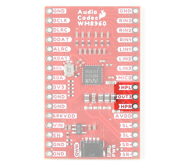
Headphones Output
The WM8960 can drive 16Ω and 32Ω headphones. The connection will depend on your setup. Make sure to check out the Headphone Output in the datasheet on page 41 for more information.
- HPL - The left headphone out will be connected to the Tip of a TRS connector.
- OUT3 - This is connected to the Sleeve of a TRS connector. If using DC blocking capacitors, connect this pin to AGND.
- HPR - The right headphone out will be connected to the Ring of a TRS connector.
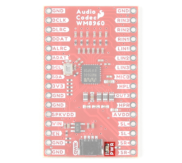
LED
The board includes one LED labeled as PWR. This indicates when there is power on the 3.3V net to power the IC's digital circuit. You can disable it with the jumper on the back of the board.
Jumpers
The following ten jumpers are included on the Audio Codec Breakout - WM8960.
- VIN, SPKVDD, and 3V3 - This 3-pad jumper allows users to select a voltage source for the speaker VDD (SPKVDD). By default, the center pad (SPKVDD) is closed on the VIN pad. Cut this trace and add a solder blob on the 3V3 side to provide SPKVDD with 3.3V. Leave both jumpers open to provide an external voltage for SPKVDD from the header pin.
- AVDD-ISO - By default, this jumper is closed. Cut this jumper to isolate AVDD from the voltage regulator to provide a VDD from the header pin.
- LED - By default, this jumper is closed and located on the bottom of the board. Cut this trace to disable the LED that is connected to the output of the 3.3V voltage regulator.
- I2C - By default, this 3-pad jumper is closed and located on the bottom of the board. The 2.2kΩ pull-up resistors are attached to the primary I2C bus; if multiple devices are connected to the bus with the pull-up resistors enabled, the parallel equivalent resistance will create too strong of a pull-up for the bus to operate correctly. As a general rule of thumb, disable all but one pair of pull-up resistors if multiple devices are connected to the bus.
For users providing their own power supply for SPKVDD and AVDD, make sure to keep the jumpers open.
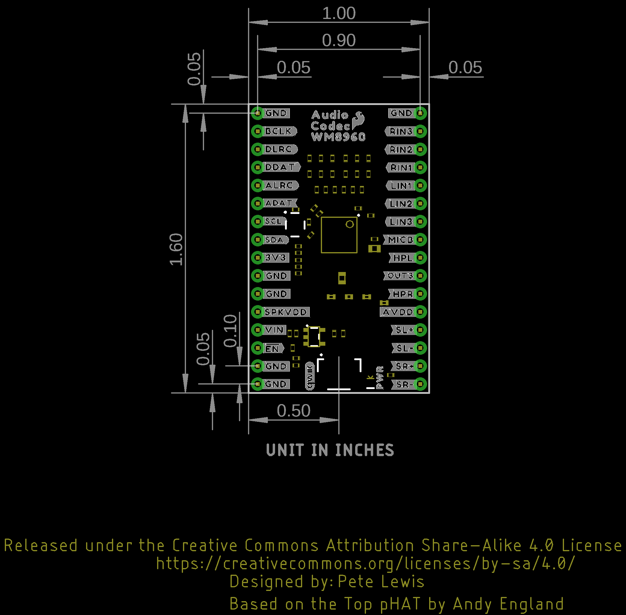
Board Dimensions
The board dimensions of the Audio Codec Breakout - WM8960 is 1.60" x 1.00".