I2C
 SFUptownMaker
 Introduction
In this tutorial, you will learn all about the I2C communication protocol, why you would want to use it, and how it's implemented.
The Inter-Integrated Circuit (I2C) Protocol is a protocol intended to allow multiple "peripheral" digital integrated circuits ("chips") to communicate with one or more "controller" chips. Like the Serial Peripheral Interface (SPI), it is only intended for short distance communications within a single device. Like Asynchronous Serial Interfaces (such as RS-232 or UARTs), it only requires two signal wires to exchange information.
Suggested Reading
Stuff that would be helpful to know before reading this tutorial:
Serial Communication
Serial Peripheral Interface (SPI)
Binary
Shift Registers
Logic Levels
Why Use I2C?
To figure out why one might want to communicate over I2C, you must first compare it to the other available options to see how it differs.
What's Wrong with Serial UART Ports?
Because serial ports are asynchronous (no clock data is transmitted), devices using them must agree ahead of time on a data rate. The two devices must also have clocks that are close to the same rate, and will remain so--excessive differences between clock rates on either end will cause garbled data.
Asynchronous serial ports require hardware overhead--the UART at either end is relatively complex and difficult to accurately implement in software if necessary. At least one start and stop bit is a part of each frame of data, meaning that 10 bits of transmission time are required for each 8 bits of data sent, which eats into the data rate.
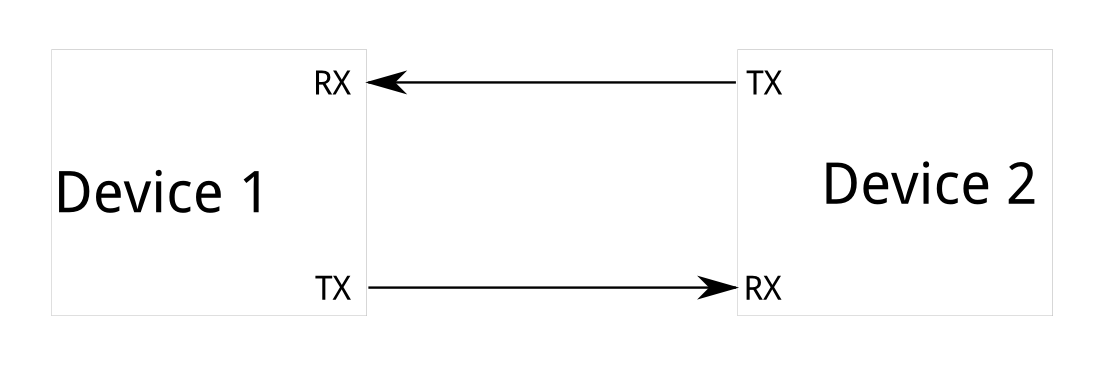
Another core fault in asynchronous serial ports is that they are inherently suited to communications between two, and only two, devices. While it is possible to connect multiple devices to a single serial port, bus contention (where two devices attempt to drive the same line at the same time) is always an issue and must be dealt with carefully to prevent damage to the devices in question, usually through external hardware.
Finally, data rate is an issue. While there is no theoretical limit to asynchronous serial communications, most UART devices only support a certain set of fixed baud rates, and the highest of these is usually around 230400 bits per second.
What's Wrong with SPI?
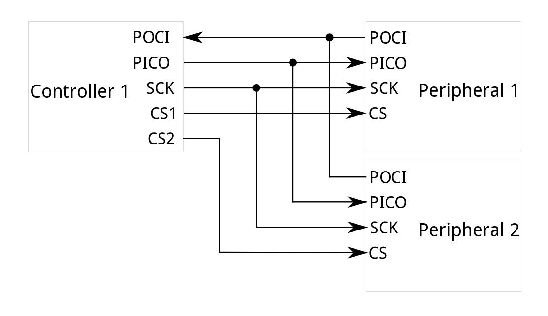
The most obvious drawback of SPI is the number of pins required. Connecting a single controller [1] to a single peripheral [1] with an SPI bus requires four lines; each additional peripheral device requires one additional chip select I/O pin on the controller. The rapid proliferation of pin connections makes it undesirable in situations where lots of devices must be connected to one controller. Also, the large number of connections for each device can make routing signals more difficult in tight PCB layout situations.
SPI only allows one controller on the bus, but it does support an arbitrary number of peripherals (subject only to the drive capability of the devices connected to the bus and the number of chip select pins available).
SPI is good for high data rate full-duplex (simultaneous sending and receiving of data) connections, supporting clock rates upwards of 10MHz (and thus, 10 million bits per second) for some devices, and the speed scales nicely. The hardware at either end is usually a very simple shift register, allowing easy implementation in software.
Enter I2C - The Best of Both Worlds!
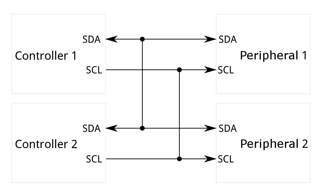
I2C requires a mere two wires, like asynchronous serial, but those two wires can support up to 1008 peripheral devices. Also, unlike SPI, I2C can support a multi-controller system, allowing more than one controller [1] to communicate with all peripheral [1] devices on the bus (although the controller devices can't talk to each other over the bus and must take turns using the bus lines).
Data rates fall between asynchronous serial and SPI; most I2C devices can communicate at 100kHz or 400kHz. There is some overhead with I2C; for every 8 bits of data to be sent, one extra bit of meta data (the "ACK/NACK" bit, which we'll discuss later) must be transmitted.
The hardware required to implement I2C is more complex than SPI, but less than asynchronous serial. It can be fairly trivially implemented in software.
| Obsolete Name | Replacement Name |
|---|---|
| Master | Controller |
| Slave | Peripheral |
A Brief History of I2C
I2C was originally developed in 1982 by Philips for various Philips chips. The original spec allowed for only 100kHz communications, and provided only for 7-bit addresses, limiting the number of devices on the bus to 112 (there are several reserved addresses, which will never be used for valid I2C addresses). In 1992, the first public specification was published, adding a 400kHz fast-mode as well as an expanded 10-bit address space. Much of the time (for instance, in the ATMega328 device on many Arduino-compatible boards), device support for I2C ends at this point. There are three additional modes specified:
- fast-mode plus, at 1MHz
- high-speed mode, at 3.4MHz
- ultra-fast mode, at 5MHz
In addition to "vanilla" I2C, Intel introduced a variant in 1995 call "System Management Bus" (SMBus). SMBus is a more tightly controlled format, intended to maximize predictability of communications between support ICs on PC motherboards. The most significant difference between SMBus is that it limits speeds from 10kHz to 100kHz, while I2C can support devices from 0kHz to 5MHz. SMBus includes a clock timeout mode which makes low-speed operations illegal, although many SMBus devices will support it anyway to maximize interoperability with embedded I2C systems.
I2C at the Hardware Level
Signals
Each I2C bus consists of two signals: SDA and SCL. SDA (Serial Data) is the data signal and SCL (Serial Clock) is the clock signal. The clock signal is always generated by the current bus controller; some peripheral devices may force the clock low at times to delay the controller sending more data (or to require more time to prepare data before the controller attempts to clock it out). This is called "clock stretching" and is described on the protocol page.
Unlike UART or SPI connections, the I2C bus drivers are "open drain", meaning that they can pull the corresponding signal line low, but cannot drive it high. Thus, there can be no bus contention where one device is trying to drive the line high while another tries to pull it low, eliminating the potential for damage to the drivers or excessive power dissipation in the system. Each signal line has a pull-up resistor on it, to restore the signal to high when no device is asserting it low.
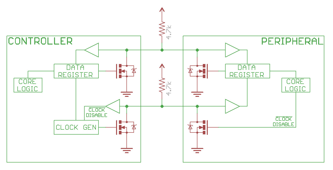
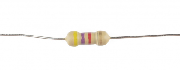
Resistor selection varies with devices on the bus, but a good rule of thumb is to start with 4.7kΩ resistor and adjust down if necessary. I2C is a fairly robust protocol, and can be used with short runs of wire (2-3m). For long runs, or systems with lots of devices, smaller resistors are better.
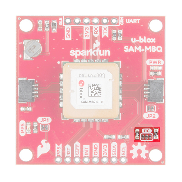
Most I2C devices offered in the SparkFun catalog usually include pull-up resistors for the SCL and SDA pins. If you have many I2C devices on the same bus, you may need to adjust the equivalent value for the pull-up resistors by disconnecting the pull-up resistors on a few of the devices. Depending on what is connected to the bus and the design, you can include about 7x I2C devices on the same bus. However, if you are having any issues, you can cut the two traces connecting to the center jumper pad using an hobby knife or remove solder on the three jumper pads using a soldering iron to disconnect the resistors on certain boards. As you can see, the design of the GPS board on the left used traces to connect the jumper pads for the pull-up resistors. The design of the GPS board on the right used solder to connect the jumper pads for the pull-up resistors.
 |
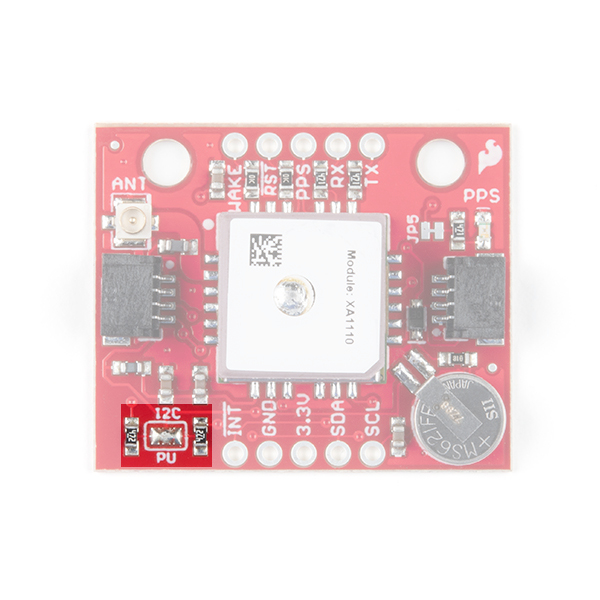 |
| Trace Connecting Jumper Pads on the SAM-M8Q | Solder Connecting Jumper Pads on the XA1110 |
If your design requires longer runs of wire, you can use a dedicated IC to extend the signal such as the PCA9615 in the following products.
SparkFun QwiicBus Hookup Guide
Qwiic Differential I2C Bus Extender (PCA9615) Hookup Guide
Signal Logic Levels
Since the devices on the bus don't actually drive the signals high, I2C allows for some flexibility in connecting devices with different I/O voltages. In general, in a system where one device is at a higher voltage than another, it may be possible to connect the two devices via I2C without any level shifting circuitry in between them. The trick is to connect the pull-up resistors to the lower of the two voltages. This only works in some cases, where the lower of the two system voltages exceeds the high-level input voltage of the the higher voltage system--for example, a 5V Arduino and a 3.3V accelerometer. Depending on the design of the Arduino or the I2C device, we recommend using a logic level converter to be consistent and avoid damaging any device on the bus.
If the voltage difference between the two systems is too great (say, 5V and 2.5V), SparkFun offers a simple I2C level shifter board — e.g. the PCA9306 Level Translator Breakout. This dedicated level shifter board the board also includes an enable line, it can be used to disable communications to selected devices. This is useful in cases where more than one device with the same address is to be connected to a single controller — Wii Nunchucks are a good example. There are also bi-directional logic level converters that can be used.
Protocol
Communication via I2C is more complex than with a UART or SPI solution. The signalling must adhere to a certain protocol for the devices on the bus to recognize it as valid I2C communications. Fortunately, most devices take care of all the fiddly details for you, allowing you to concentrate on the data you wish to exchange.
Basics
Messages are broken up into two types of frame: an address frame, where the controller indicates the peripheral to which the message is being sent, and one or more data frames, which are 8-bit data messages passed from controller to peripheral or vice versa. Data is placed on the SDA line after SCL goes low, and is sampled after the SCL line goes high. The time between clock edge and data read/write is defined by the devices on the bus and will vary from chip to chip.
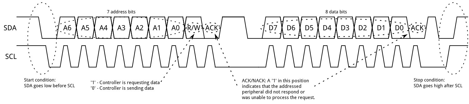
Start Condition
To initiate the address frame, the controller device leaves SCL high and pulls SDA low. This puts all peripheral devices on notice that a transmission is about to start. If two controllers wish to take ownership of the bus at one time, whichever device pulls SDA low first wins the race and gains control of the bus. It is possible to issue repeated starts, initiating a new communication sequence without relinquishing control of the bus to other controller(s); we'll talk about that later.
Address Frame
The address frame is always first in any new communication sequence. For a 7-bit address, the address is clocked out most significant bit (MSB) first, followed by a R/W bit indicating whether this is a read (1) or write (0) operation.
The 9th bit of the frame is the NACK/ACK bit. This is the case for all frames (data or address). Once the first 8 bits of the frame are sent, the receiving device is given control over SDA. If the receiving device does not pull the SDA line low before the 9th clock pulse, it can be inferred that the receiving device either did not receive the data or did not know how to parse the message. In that case, the exchange halts, and it's up to the controller of the system to decide how to proceed.
Data Frames
After the address frame has been sent, data can begin being transmitted. The controller will simply continue generating clock pulses at a regular interval, and the data will be placed on SDA by either the controller or the peripheral, depending on whether the R/W bit indicated a read or write operation. The number of data frames is arbitrary, and most peripheral devices will auto-increment the internal register, meaning that subsequent reads or writes will come from the next register in line.
Stop condition
Once all the data frames have been sent, the controller will generate a stop condition. Stop conditions are defined by a 0->1 (low to high) transition on SDA after a 0->1 transition on SCL, with SCL remaining high. During normal data writing operation, the value on SDA should not change when SCL is high, to avoid false stop conditions.
Advanced Protocol Topics
10-bit Addresses
In a 10-bit addressing system, two frames are required to transmit the peripheral address. The first frame will consist of the code b11110xyz, where 'x' is the MSB of the peripheral address, y is bit 8 of the peripheral address, and z is the read/write bit as described above. The first frame's ACK bit will be asserted by all peripherals which match the first two bits of the address.
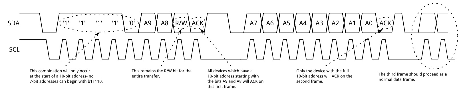
As with a normal 7-bit transfer, another transfer begins immediately, and this transfer contains bits 7:0 of the address. At this point, the addressed peripheral should respond with an ACK bit. If it doesn't, the failure mode is the same as a 7-bit system.
Note that 10-bit address devices can coexist with 7-bit address devices, since the leading '11110' part of the address is not a part of any valid 7-bit addresses.
Repeated Start Conditions
Sometimes, it is important that a controller be allowed to exchange several messages in one go, without allowing other controllers on the bus to interfere. For this reason, the repeated start condition has been defined.
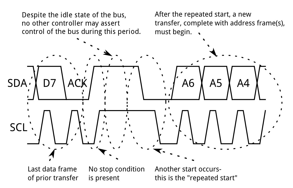
To perform a repeated start, SDA is allowed to go high while SCL is low, SCL is allowed to go high, and then SDA is brought low again while SCL is high. Because there was no stop condition on the bus, the previous communication wasn't truly completed and the current controller maintains control of the bus.
At this point, the next message can begin transmission. The syntax of this new message is the same as any other message--an address frame followed by data frames. Any number of repeated starts is allowed, and the controller will maintain control of the bus until it issues a stop condition.
Clock Stretching
At times, the controller's data rate will exceed the peripheral's ability to provide that data. This can be because the data isn't ready yet (for instance, the peripheral hasn't completed an analog-to-digital conversion yet) or because a previous operation hasn't yet completed (say, an EEPROM which hasn't completed writing to non-volatile memory yet and needs to finish that before it can service other requests).

In this case, some peripheral devices will execute what is referred to as "clock stretching". Nominally, all clocking is driven by the controller — peripherals simply put data on the bus or take data off the bus in response to the controller's clock pulses. At any point in the data transfer process, an addressed peripheral can hold the SCL line low after the controller releases it. The controller is required to refrain from additional clock pulses or data transfer until such time as the peripheral releases the SCL line.
CCS811 Air Quality Breakout Hookup Guide
Interested in learning more foundational topics?
See our Engineering Essentials page for a full list of cornerstone topics surrounding electrical engineering.
Qwiic Connect System
The SparkFun Qwiic Connect System was developed by Nate in SparkX and released in 2017. If you are unfamiliar, the Qwiic Connect System is an ecosystem of I2C sensors, actuators, shields, cables and more, that make prototyping faster and less prone to error.

All Qwiic-enabled boards use a common 1 mm pitch, 4-pin JST connector which takes out the extra steps required to solder and strip wires between boards. The connector reduces the amount of required PCB space, and polarized connections mean you can’t hook it up wrong. Boards can be daisy chained together which allows multiple devices to be connected on the same bus. For more information, check out the Qwiic's Frequently Asked Questions or the video below!

no soldering
Qwiic cables (4-pin JST) plug easily from development boards to sensors, shields, accessory boards and more, making easy work of setting up a new prototype.
polarized connector
There's no need to worry about accidentally swapping the SDA and SCL wires on your breadboard. The Qwiic connector is polarized so you know you’ll have it wired correctly every time, right from the start.
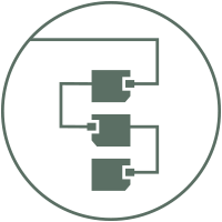
daisy chain-able
It’s time to leverage the power of the I2C bus! Most Qwiic boards will have two or more connectors on them, allowing multiple devices to be connected.
Resources and Going Further
I2C is a relatively complex interface, and there are many resources out there to help you deal with it. Below are some of the more informative ones.
- Wikipedia Article on I2C - Not great, but not a terrible place to start.
- Standards Doc - Phillips Semiconductor became NXP a few years back; this is the official standards doc for I2C.
- I2C primer - The official primer on I2C and related technologies.
- Linux Tools for I2C - A nice set of tools for working with I2C and related buses in embedded Linux environments, like pcDuino or Raspberry Pi.
- Open Source Hardware Association: A Resolution to Redefine SPI Signal Names
- Qwiic Connect System
To use I2C over long distances, check out the dedicated PCA9615 differential I2C bus extender.
Qwiic Differential I2C Bus Extender (PCA9615) Hookup Guide
Or check out our SPI and I2C tutorial with a Raspberry Pi.
Raspberry Pi SPI and I2C Tutorial
Need some inspiration for your next project? Check out some of these related tutorials:
Qwiic HAT for Raspberry Pi Hookup Guide
SparkFun Qwiic MicroPressure Hookup Guide
Qwiic 6DoF - ISM330DHCX Hookup Guide
Getting Started with u-blox Thingstream and PointPerfect
Looking for more inspiration? Check out some of these blog posts for ideas: