GNSS Correction Data Receiver (NEO-D9S) Hookup Guide
 bboyho,
  PaulZC
Hardware Overview
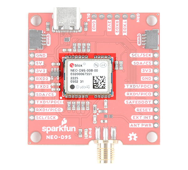
The NEO-D9S-00B is a satellite data receiver for L-band correction broadcast, which can be configured for use with a variety of correction services. It decodes the satellite transmission and outputs a correction stream, enabling a high precision GNSS receiver to reach accuracies down to centimeter level! In this section, we'll highlight important parts of the board. For more information about the NEO-D9S, check out the Resources and Going Further for more information.
Power
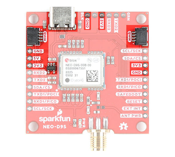
Power for this board is 3.3V and we have provided multiple power options. This first and most obvious is the USB-C connector. Secondly, are the Qwiic Connectors on the left and right of the board for ground and 3.3V. Thirdly, there is a 5V pin on the PTH header along the left side of the board that is regulated down to 3.3V with the 3.3V/600mA AP2112K voltage regulator (as indicated with the 5-pin component next to the 3V3 pin). Make sure that power you provide to this pin does not exceed 6 volts. Just below the 5V pin is a 3V3 pin that should only be provided a clean 3.3V power signal. 3V3 are also broken out on the USB-to-serial port and on the other side of the board. GND is also provided near each power pin.
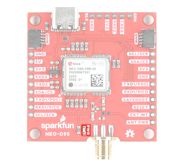
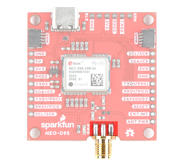
LED
There is one power LED labeled as PWR. The LED will illuminate when 3.3V is activated. This can be disabled by cutting the jumper on the back of the board labeled as "PWR" as well.
Qwiic and I2C
There are two pins labeled SDA and SCL which indicates the I2C data and clock lines. Similarly, you can use either of the Qwiic connectors to provide power and utilize I2C. The Qwiic ecosystem is made for fast prototyping by removing the need for soldering. All you need to do is plug a Qwiic cable into the Qwiic connector and voila!
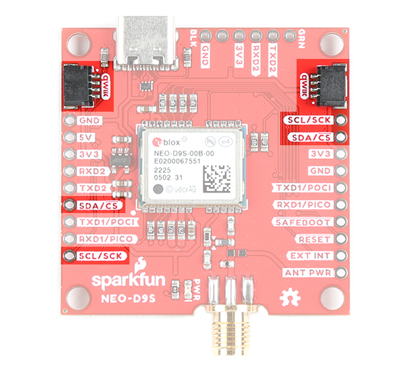
SPI
There are four pins that are labeled with their corresponding SPI functionality. These pins are broken out on both sides of the board. As mentioned in the jumpers section, you'll need to close the SPI jumper on the underside to enable SPI.
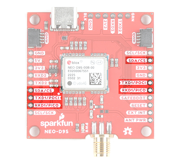
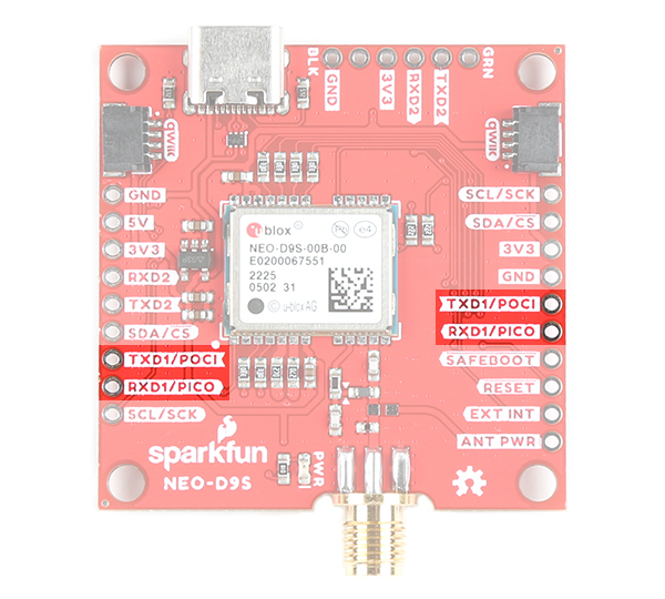
UART
There are two pins labeled as TXD1/POCI and RXD1/PICO. The UART pins are shared with the SPI pins. By default, the UART interface is enabled. Be sure that the SPI jumper on the back of the board is open.
- TXD1/POCI = TX out from NEO-D9S
- RXD1/PICO = RX into NEO-D9S
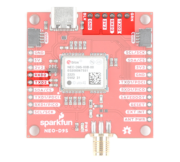
There is also a second UART port. You can connect this to a u-blox F9 module that supports correction data output from the NEO-D9S. The datasheet indicates that you could potentially use any high precision GNSS receiver from the u-blox F9 platform as denoted as the ZED-F9X, where the "X" indicates different variant. Make sure to check the latest u-blox F9 product Integration Manual for more information on whether the correction data is supported with the respective module
Broken Out Pins
There are four other pins broken out:
- SAFEBOOT: The safeboot pin (
SAFEBOOT) is used to start up the IC in safe boot mode, this could be useful if you somehow manage to corrupt the module's Flash memory. - RESET: The reset pin (
RESET) resets the chip. - EXT INT: The interrupt pin (
EXT INT) can be used to wake the chip from power save mode. - ANT PWR: The antenna power pin (
ANT PWR) is available for advanced users that want to power their L-band 3.3V active antenna with an external power source.- Isolate VCC_RF: You will need to isolate the VCC_RF. Users will need to make sure to cut the trace between the two arrows (i.e. ▶ ◀) to disable the VCC_RF antenna power. You can also shift the surface mount component that connects to the trace by moving it so that it does not connect to the SMA connector.
- Install SMD Component: You will then need to populate the board where L1 is located (i.e. the pads that are not currently populated and connects to the ANT PWR PTH) with a 0603 part with impedance >500 Ohms at 1.5GHz.
- Inject Power: When ready, connect a clean DC power supply voltage between ANT PWR and GND.
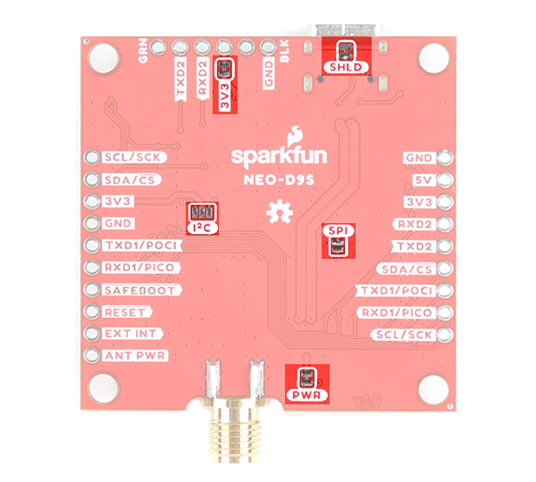
Jumpers
If you flip the board over, you will notice a few jumper pads. For more information on modifying the jumpers, check out our tutorial on working with jumper pads and PCB traces.
- SHLD: This jumper connects the USB Type C connector's shield pin to GND. Cut this to isolate the USB Type C connector's shield pin.
- 3V3: This jumper connects 3.3V to the UART2 port. By default, this is closed and will provide power to the your GNSS receiver. Cut this jumper if you are connecting a 3.3V USB-to-Serial converter with its own power source, or if the GNSS receiver is being powered with its own power source.
- I2C: This three way jumper labeled
I2Cwill connect to two pull-up resistors to the I2C data and clock lines when closed. For users with that do not have pull-up resistors attached to the I2C lines on their microcontroller, make sure to close the jumpers with a little solder blob. - PWR: The jumper labeled
PWRconnects to the power LED. If you cut this trace, it will disconnect the Power LED. - SPI: The jumper labeled
SPIenables the SPI data bus, thus disabling the UART functions on those lines. This also disables I2C interface.
SMA Connector
The board is equipped with a SMA connector. You will need an active antenna that can receive signals from an L-Band satellite between 1525.0 MHz to 1559.0 MHz as stated in the datasheet. The specific frequency between the L-Band that the NEO-D9S uses depends on your region and service provider. Make sure to check the antenna's datasheet, region, and service provider for more information.
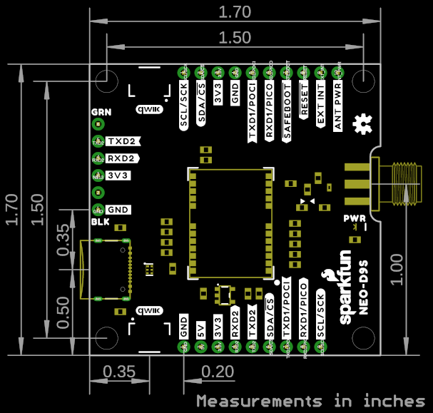
Board Dimensions
The board dimensions are 1.70"x1.70". This does not include the dimensions for the SMA connector and USB Type C connector. There are four mounting holes by each corner of the board.