SparkFun Qwiic 3-Axis Accelerometer (ADXL313) Hookup Guide
 QCPete
Hardware Overview
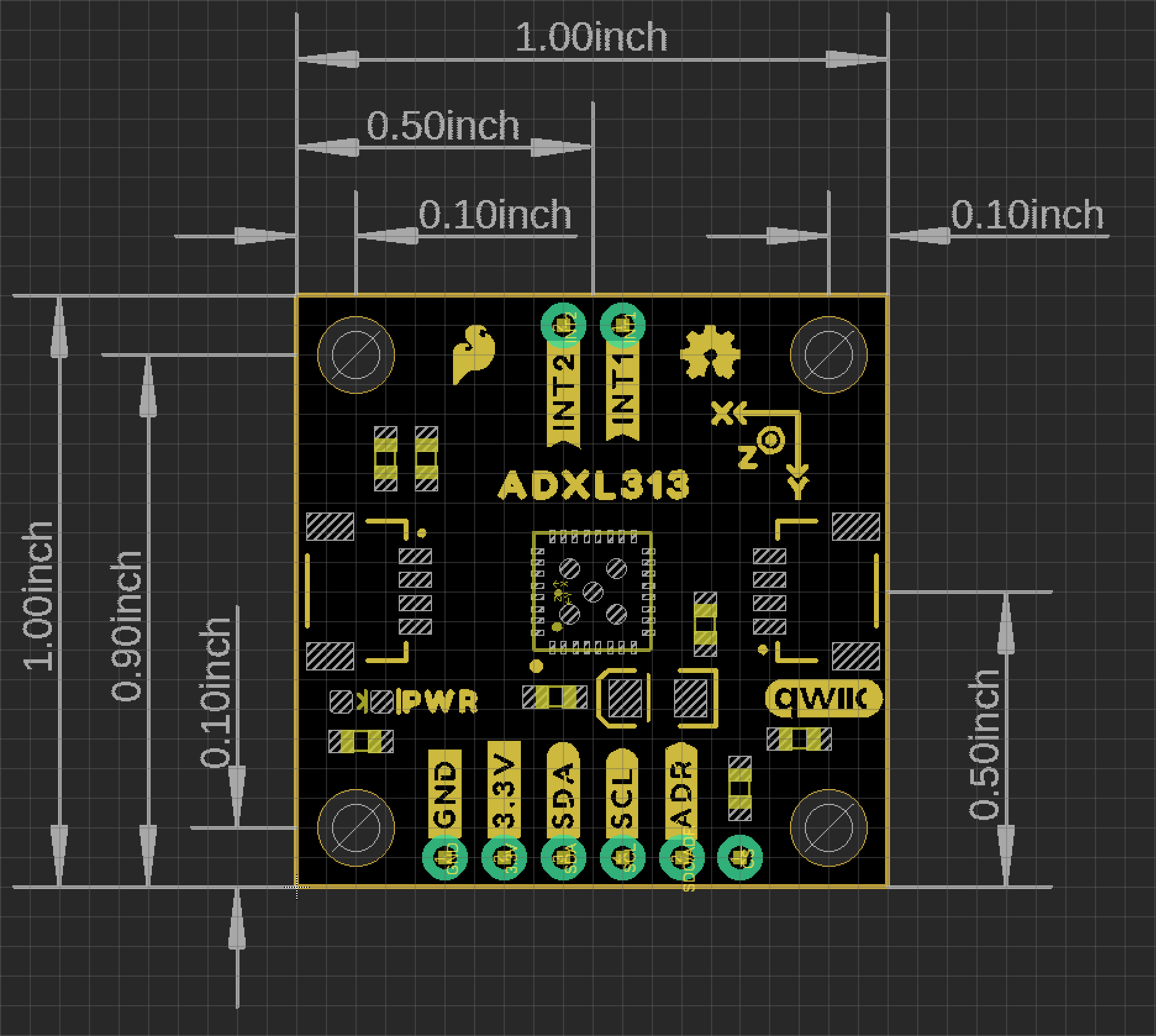
Board Dimensions
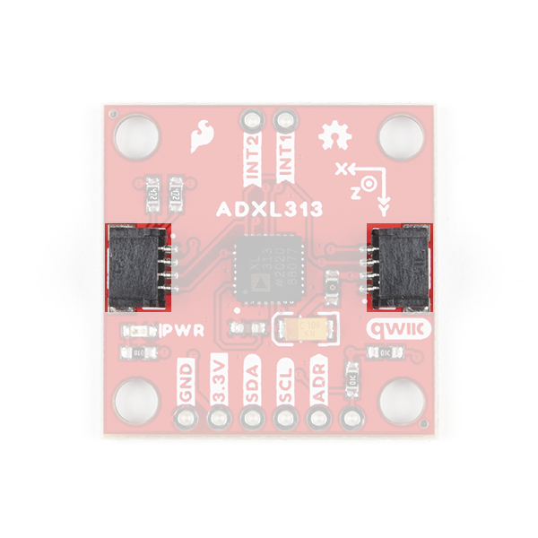
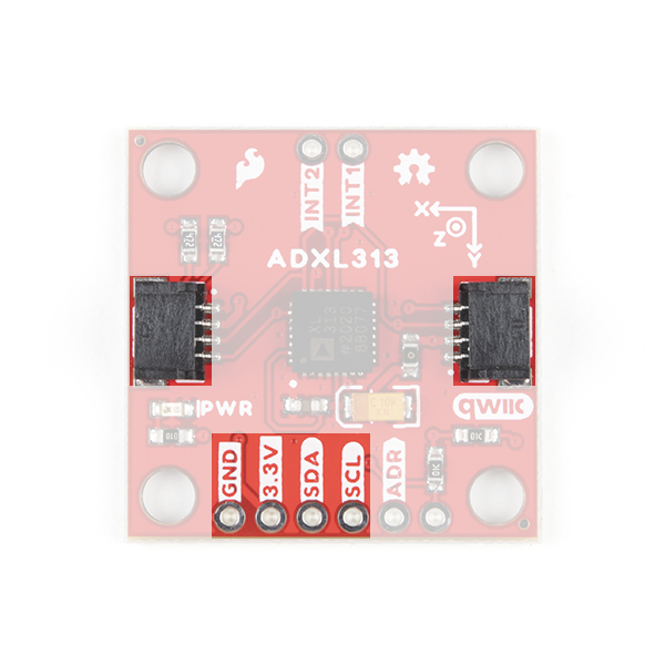
The SparkFun 3-Axis Digital Accelerometer Breakout - ADXL313 (Qwiic) is laid out on the standardized 1" x 1" (2.54 x 2.54 cm) Qwiic breakout board and includes the standard four 0.13" mounting holes, which are compatible with 4-40 screws.
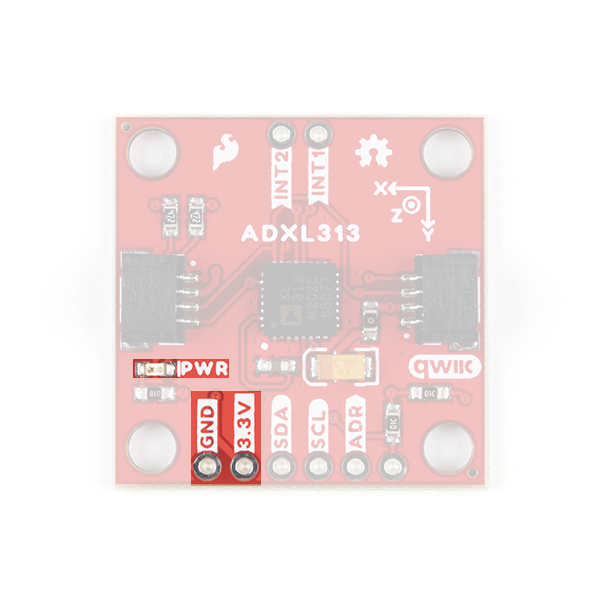
Power
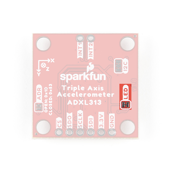
There is a power status LED to help make sure that your Qwiic ADXL313 Accelerometer is getting power. You can power the board either through the polarized Qwiic connector system or the breakout pins (3.3V and GND) provided. The Qwiic system is meant to run on 3.3V, be sure that you are NOT using another voltage when using the Qwiic system. A jumper is available on the back of the board to remove power to the LED for low-power applications (see Jumpers section below).
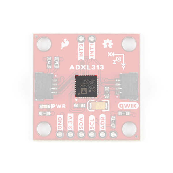
ADXL313 Accelerometer
The ADXL313 accelerometer from Analog Devices is a low cost, low power, up to 13-bit resolution, 3-axis accelerometer with a 32-level FIFO stack capable of measuring up to ±4g. The shock rating for the sensor (IC only, not board) is up to 10,000g, which is great for data loggers like black boxes. The sensor also has automotive applications including car alarms, hill start aid (HSA) systems, and electronic parking brakes.
Theory of Operation
The sensor mechanism contains a polysilicon structure built above a silicon wafer. The polysilicon structure includes a central mass with springs to suspend it over the surface of the wafer. An acceleration creates a deflection of the structure, which is measured with differential capacitors, resulting in a sensor output whose amplitude is proportional to acceleration. Phase-sensitive demodulation is used to determine the magnitude and polarity of the acceleration.
For more details, check out these articles from Analog Devices:
- Dual Axis, Low g, Fully Integrated Accelerometers
- Sonic Nirvana: Using MEMS Accelerometers as Acoustic Pickups in Musical Instruments
Sensor Characteristics
Below, is a table of the characteristics of the accelerometer. For more details, please refer to the datasheet.
| Characteristic | Description |
|---|---|
| Power |
Supply Voltage: 2.0 - 3.6V Supply Cuurent:
|
| Measurement Range | ±.5g, ±1g, ±2g, ±4g |
| Resolution |
All Ranges: 10 bits (Default) ±.5g Range: 10 bits (Full Resolution) ±1g Range: 11 bits (Full Resolution) ±2g Range: 12 bits (Full Resolution) ±4g Range: 13 bits (Full Resolution) |
| FIFO Stack | 32 levels |
| Data Rate | 6.25 - 3200Hz |
| I2C Address (7-bit) | 0x1D (Default), 0x53 |
| SPI Configuration | 3-wire or 4-wire Operation |
Power Modes
By default, with standard operation, the ADXL313 automatically modulates its power consumption based on the output data rate. For increased power savings, an optional low power mode is available for data rates below 400 Hz. The available power savings for the low power mode (VS = 3.3V) is detailed in the table below. In addition, there are two power configurations for minimal power consumption. For more details, please refer to the datasheet.
| Output Data Rate (Hz) | Bandwidth (Hz) | Current Consumption (at VS = 3.3V): IDD (µA) | |
|---|---|---|---|
| Std. Operation | Low Power Mode | ||
| 3200 | 1600 | 170 | --- |
| 1600 | 800 | 115 | --- |
| 800 | 400 | 170 | --- |
| 400 | 200 | 170 | 115 |
| 200 | 100 | 170 | 82 |
| 100 | 50 | 170 | 65 |
| 50 | 25 | 115 | 57 |
| 25 | 12.5 | 82 | 50 |
| 12.5 | 6.25 | 65 | 43 |
| 6.25 | 3.125 | 57 | --- |
Autosleep Mode
Autosleep mode provides additional power savings by automatically switching the ADXl313 into sleep mode during periods of inactivity. The inactivity level is determined by two factors, a threshold value and a time period. Based upon their configuration, if the sensor doesn't detect an acceleration in excess of the threshold value for the specified time period, the ADXL313 will automatically transition into sleep mode.
Standby Mode
Placing the ADXL313 into standby mode discontinues any measurements, preserves the contents of the FIFO stack, and reduces current consumption down to 0.1 µA.
FIFO Operation
The ADXL313 includes a 32-level FIFO stack management system that is utilized to minimize the burden on the host microcontroller. The buffer has four different modes of operation: Bypass, FIFO, Stream, and Trigger. For more details, please refer to the datasheet.
Note: For users unfamiliar with how a FIFO typically operates, check out this example from the Qwiic Keypad hookup guide.
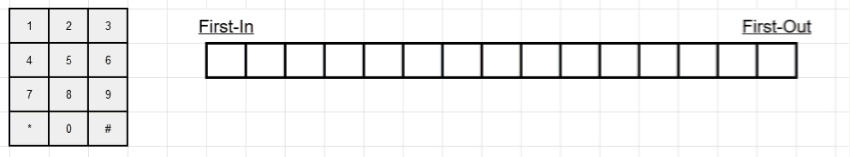
Demonstration of the FIFO: (1) Filling the FIFO stack with inputs, (2) overwriting old inputs, and (3) incrementing & reading the FIFO.
Bypass Mode
The FIFO is bypassed and no values are stored.
FIFO Mode
The FIFO collects up to 32 values and then stops collecting data and triggers the watermark interrupt, collecting new data only when FIFO is not full. The accelerometer will continue to operate after the FIFO is full, so that features such as activity detection can still be utilized. The watermark interrupt will continue to trigger until the number of samples in FIFO is less than the threshold.
Stream Mode
The FIFO holds the latest 32 data values. When FIFO is full, the oldest data is overwritten with newer data and the watermark interrupt will trigger. The watermark interrupt will continue to trigger until the number of samples in FIFO is less than the threshold.
Trigger Mode
When triggered by the trigger bit, FIFO holds the last data samples before the trigger event and then continues to collect data until full. New data is collected only when FIFO is not full. Additional trigger events will not function in this mode until the trigger mode is cleared.
Self Test Operation
A unique feature of the ADXL313 is the self test operation, which can test the sensor's mechanical and electronic systems simultaneously. When enabled, an electrostatic force is exerted on the mechanical sensor and moves the mechanical sensing element in the same manner as an acceleration would. This creates an additive acceleration that is proportional to VS2. For more details, please refer to the datasheet.
Qwiic and I2C
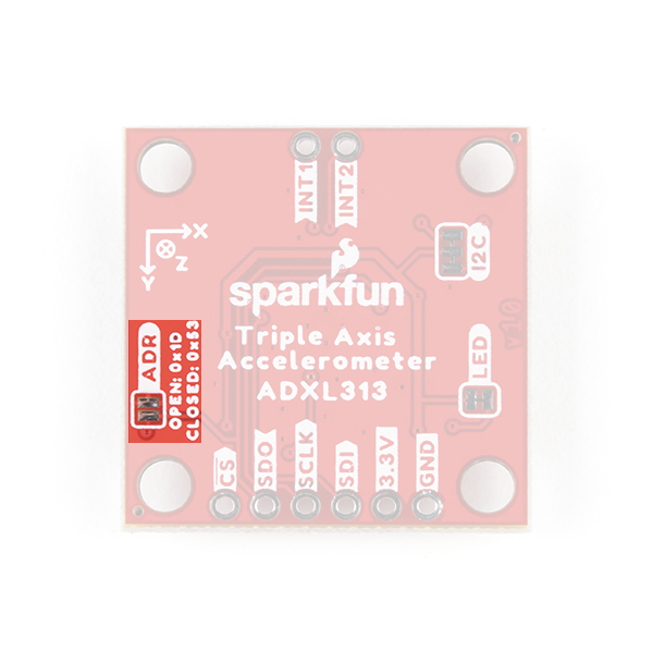
I2C Address
The Qwiic ADXL313 Accelerometer’s I2C address, 0x1D (7-bit), is factory set. An alternate I2C address of 0x53 (7-bit) can be configured by modifying the ADDR jumper or by pulling the ADR pin low.
Qwiic Connectors
The simplest way to use the Qwiic ADXL313 Accelerometer is through the Qwiic connect system. The connectors are polarized for the I2C connection and power. (*They are tied to the corresponding power and I2C breakout pins.)
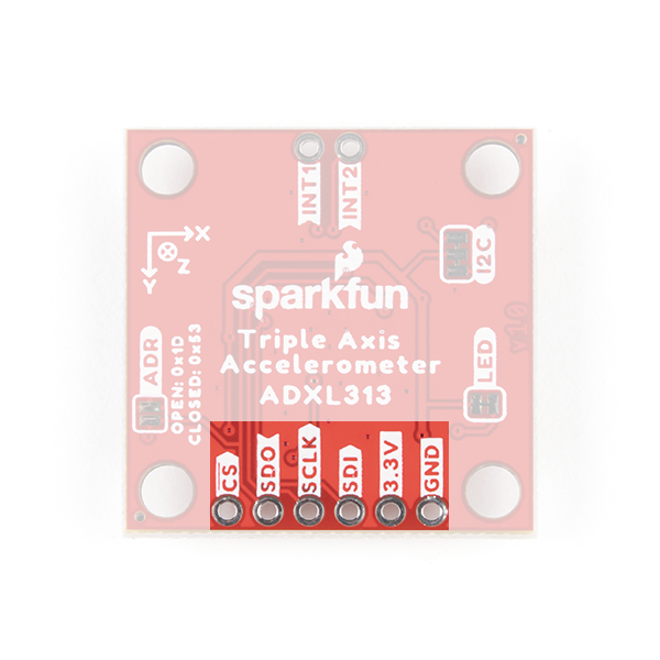
Breakout Pins
The board also provides eight labeled breakout pins.

I2C
You can connect these lines to the I2C bus of your microcontroller and power pins (3.3V and GND), if it doesn't have a Qwiic connector. The interrupt pins are also broken out to use for triggered events.
SPI
You can connect these lines to the SPI bus of your microcontroller and power pins (3.3V and GND); the sensor can operate in either a 3-wire or 4-wire configuration. The interrupt pins are also broken out to use for triggered events.
Interrupt Pins
The interrupt pins (active high) are used to indicate various states of the ADXL313, depending on how they are configured and if they are enabled. The interrupt pins can be configured for the following modes:
- Activity - Triggers when the acceleration is greater than a stored threshold.
- Inactivity - Triggers when the acceleration is lower than a store threshold for a specified amount of time (up to 255 seconds).
- Watermark - Triggers when the number of samples stored in the FIFO reaches a specific value.
- Overrun - Triggers when the FIFO is overrun (new data replaces unread data in the stack).
Additionally, the interrupts can be used to trigger measurements into the FIFO, when the FIFO is configured for Trigger Mode.

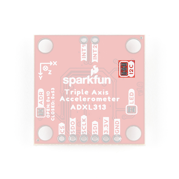
Jumpers
There are three jumpers on the board. Not sure how to cut or modify a jumper? Read here!
Power LED
Cutting the LED jumper will remove the 1kΩ resistors and PWR LED from the 3.3V power. This is useful for low power applications.
I2C Pull-Up
Cutting the I2C jumper will remove the 4.7kΩ pull-up resistors from the I2C bus. If you have many devices on your I2C bus you may want to remove these jumpers.
Address Pull-up
Soldering the ADR jumper connect a 10kΩ pull-up resistor to the SDO/ADR pin. This can be used to configure the default I2C address of the device to 0x53 (7-bit) on power up.