Qwiic Keypad Hookup Guide
 QCPete, santaimpersonator
Hardware Overview
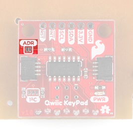
Keypad
This is a basic 12 button keypad that has been designed for easy user input and functionality. The buttons are set up in a matrix format. This allows the ATtiny84 to scan the 7 output pins to see which of the 12 buttons are being pressed.
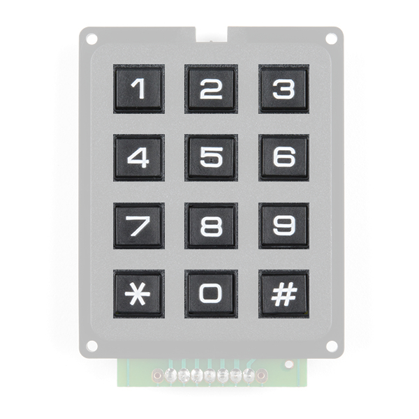
Each of the keypad's 12 buttons has been labeled 1, 2, 3, 4, 5, 6, 7, 8, 9, 0, *, and # and has been formatted to into the same layout as a telephone keypad. Each keypress resistance ranges between 10 - 150Ω.
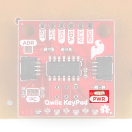
Power LED
There is a power status LED to help make sure that your Qwiic Keypad is getting power. You can power the board either through the polarized Qwiic connector system or the breakout pins (PWR and GND) provided. The Qwiic system is meant to run on 3.3V, be sure that you are NOT using another voltage when using the Qwiic system. Qwiic Keypad is very low power and uses less than 4mA at 3.3V.
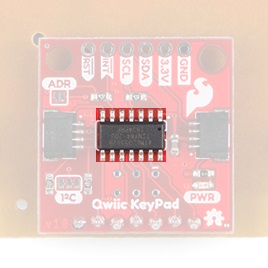
ATtiny84
With the pre-installed firmware, the ATtiny84 acts as an intermediary (microcontroller) multiplexing the buttons for inputs. This allows the Qwiic Keypad to store the button presses in the FIFO stack to be read over I2C. Although the ATtiny84 has a wide voltage range, since this is a Qwiic product, users should power the board with the labeled 3.3V.
First-In, First-Out (FIFO) Stack
In the firmware, the FIFO stack stores the most recent 15 button inputs. Once the stack is full, any previous inputs are overwritten. The FIFO stack is manually incremented using the FIFO Command register. If there are no more values stored in the FIFO stack, the output will be 0x00 or Null.
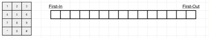
The condition for a FIFO incrementation is a request event (register is read) after the updateFIFO register has already been set to 0x01.
Order of operations for FIFO incrementation:
- Input: Set updateFIFO register to 0x01.
- Firmware: Wait for request event.
- Input: Create a request event (read a register).
- Firmware:
- Set updateFIFO register to 0x00.
- Increment new index for the FIFO buffer.
- Determines the "next button" value.
- Calculates time since the "next button" was pressed.
- Updates register with new values (for the "next button" and time since the "next button" was pressed).
- Input: Wait for next updateFIFO command.
Qwiic and I2C
I2C Address
In the firmware, the Qwiic Keypad’s I2C address is configurable so you can add a bunch of them to the same bus without collision issues.
Factory Default I2C Slave Address: 0x4B
I2C Registers
| Address | Description |
|---|---|
| 0x00 | Default I2C Slave Address (Stored in EEPROM) |
| 0x01 - 0x02 | Firmware Version (MSB First) |
| 0x03 | Oldest Button Press (aka First-Out from FIFO stack) |
| 0x04 - 0x05 | Time in ms since the button was pressed (MSB First, 16-bit = Max Value of 65,535 ms). |
| 0x06 | FIFO Increment Command: Set bit 0 to increment FIFO. |
| 0x07 | Current/Set I2C Slave Address (Write). Stored in EEPROM. |
Connections
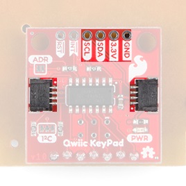
The simplest way to use the Qwiic Keypad is through the Qwiic connect system. The connectors are polarized for the I2C connection and power. (*They are tied to their corresponding breakout pins.)
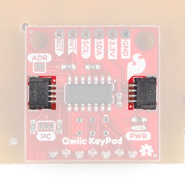
However, the board also provides six labeled breakout pins. You can connect these lines to the I2C bus of your microcontroller and power pins (3.3V and GND), if it doesn't have a Qwiic connector. The interrupt and reset pins are also broken out to use for triggered events.
Interrupt Pin
The interrupt pin (active low) is used to indicate that there are available entries in the FIFO stack. Effectively, if it is tied to an interrupt on your microcontroller and you are using it to increment the FIFO stack, then it will get triggered every time a button is pressed. The INT pin is pulled up with a 4.7kΩ resistor and will be low if there are entries. The INT pin will return high once the FIFO has been cleared.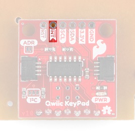
Reset Pin
Reset pin tied to the reset pin on the ATtiny. When pulled low, this will effectively reset the Qwiic Keypad and restart the device, loading the I2C address that was stored in EEPROM. It is mostly, broken out for reprogramming the ATtiny84.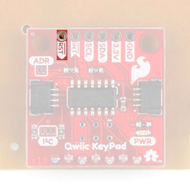
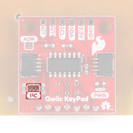
Jumpers
There are jumpers on the board allowing the user to select between different I2C addresses as well as to remove the pull up resistors from the I2C pins, if needed.
I2C Address
Bridging the I2C address jumper changes the slave address from the value stored in EEPROM to the I2C Jumper Default (or alternate): 0x4A.
- Open/Cut: Factory or Set I2C Slave Address: 0x4B (Factory Set) or 0x## (User Set)
- Bridged: I2C Jumper Default Slave Address: 0x4A (Alternate)
I2C Pull-Up
Cutting the I2C jumper will remove the 2.2kΩ pull-up resistors from the I2C bus. If you have many devices on your I2C bus you may want to remove these jumpers. Not sure how to cut a jumper? Read here!