Cellular Function Board - Blues Wireless Notecarrier
 El Duderino
Hardware Overview
Let's take a closer look at the Notecard module and other hardware present on this Function Board.
Blues Wireless Notecard - NOTE_NBGL-500
The Blues Wireless Notecard module offers a low-power cellular connection from a connected device to the cloud through either the Notehub service or alternate cellular service with a supported external SIM. The module has a built-in SIM card that includes a 10 year subscription and 500MB of data in the initial purchase price. The built-in SIM on the Notecard works in over 140 countries with varying levels of cellular coverage, for a complete list of compatible countries, refer to the Cellular Service section of the Notecard datasheet. The Cellular Function Board ships with the NOTE_NBGL-500 Notecard which operates over narrowband global networks (LTE-M, NB-IoT and GPRS).
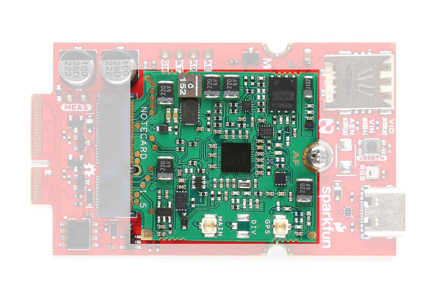
The Notecard uses the BG95-M3 cellular module with integrated GNSS from Quectel. The GNSS supports GPS, GLONASS, BeiDou, Galileo and QZSS constellations. The Notecard also has an on-board 3-axis accelerometer with an on-chip temperature sensor. For a complete overview of the Notecard, refer to the datasheet.
USB-C Connector
The USB-C connector provides a direct serial interface with the Notecard over a USB connection.
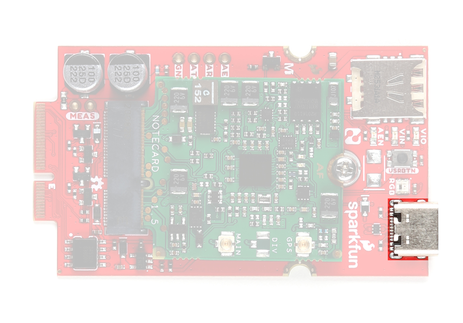
This connection allows you to use the Notecard with Blues Wireless' browser-based CLI, Notecard Playground. This CLI is very helpful for configuring and testing the Notecard quickly over USB. Those who prefer to download and use the CLI application locally can find it here.
Nano-SIM Slot
The Function board includes a Nano-SIM slot for users who prefer to use their own nano SIM card instead of the built-in one on the Notecard module.
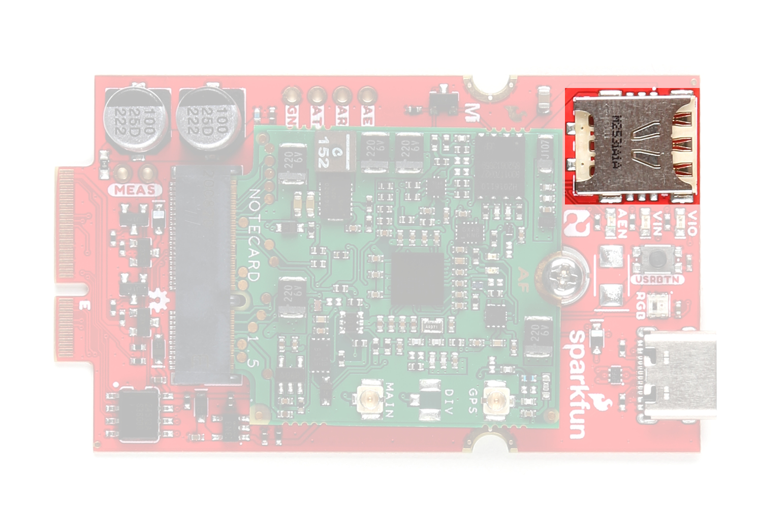
Enabling the external SIM capability requires updating several settings on the Notecard. Refer to this guide from Blues Wireless for detailed instructions for configuring the Notecard to work with an external SIM card. Reminder, this Function Board uses the NOTE_NBGL-500 Notecard so it only supports narrowband LTE networks (no 3G or 4G networks).
AUX UART PTH Header
The Function Board routes the auxiliary UART pins used for Outboard DFU on the Notecard to a 0.1"-spaced PTH header along with the Auxiliary Enable pin.

This interface allows for users to connect directly to the Notecard's auxiliary UART (AUX RX and AUX TX) as well as the Auxiliary Enable pin to toggle the auxiliary UART. The Function Board also routes the AUX1 to a pushbutton labeled "USRBTN" to allow for a user-configurable manual input on that pin.
LEDs
The board has three power indication LEDs labeled VIO, VIN, and AEN as well as a WS2812 RGB LED tied to the Notecard's AUX2 pin.
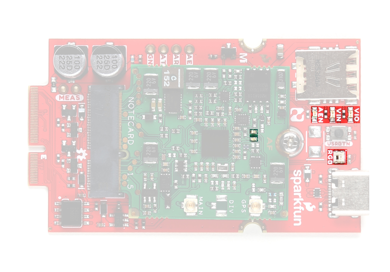
- VIO - 3.3V I/O voltage status. LED turns on when 3.3V from the MicroMod connector is present.
- VIN - Notecard power status. LED turns on when the Notecard is powered.
- AEN - Auxiliary UART status. LED turns on when the AEN pin is pulled HIGH to enable the auxiliary UART on the Notecard.
- RGB - AUX2 RGB LED. The data input for the WS2812 LED connects to AUX2 on the Notecard to allow for user-configured LED statuses. The data input also connects to F5 on the Function Board's MicroMod M.2 connector for users who prefer to manipulate the LED through a connected Processor.
The Notecard has two LEDs. The green LED reports modem activity and the red LED reports user activity.
Solder Jumpers
The Function Board has eight solder jumpers labeled: SHLD, VIO_LED, PWR_LED, AUX_EN_LED, RGB, ANT_PWR, WP, and MEAS
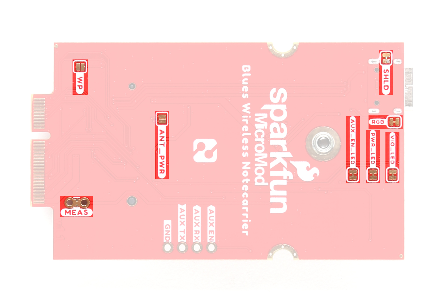
The table below outlines the jumpers labels, functions, default states and any notes regarding their behavior.
| Jumper Label | Default State | Function | Notes |
|---|---|---|---|
| SHLD | CLOSED | Connects USB-C Shield pin to Ground. | Manipulate this jumper to adjust whether or not the USB-C cable shield pin connects to the PCB's ground plane. |
| VIO_LED | CLOSED | Completes VIO status LED circuit. | Open to disable the labeled LED. |
| PWR_LED | CLOSED | Completes Notecard Power status LED circuit. | |
| AUX_EN_LED | CLOSED | Completes Auxiliary Enable status LED circuit. | |
| RGB | CLOSED | Completes the RGB LED circuit. | |
| ANT_PWR | OPEN | Enables power for external antenna. | Close to enable power for using an active GNSS antenna. |
| WP | OPEN | EEPROM write protection. | Close to disable write protection for the EEPROM IC. |
| MEAS | CLOSED | Measure Function Board current draw. | Open the jumper and use a digital multimeter to measure the current draw of the Function Board. Note, opening this jumper interrupts the voltage input circuit. |
MicroMod Pinout
As mentioned previously, we recommend using this Function Board with the latest versions of the MicroMod Single Main Board and Double Main Board as the revisions benefit this Function Board and the recommended STM32 Processor. Check out the MicroMod Main Board Hookup Guide v2 for details on all changes made to these Main Boards. The tables below outline the complete MicroMod Pinout and pins used by the Cellular Function Board:
| AUDIO | UART | GPIO/BUS | I2C | SDIO | SPI0 | Dedicated |
| Function | Bottom Pin |
Top Pin |
Function | ||||||
|---|---|---|---|---|---|---|---|---|---|
| (Not Connected) | 75 | GND | |||||||
| 3.3V | 74 | 73 | G5 / BUS5 | ||||||
| RTC_3V_BATT | 72 | 71 | G6 / BUS6 | ||||||
| SPI_CS1# | SDIO_DATA3 (I/O) | 70 | 69 | G7 / BUS7 | |||||
| SDIO_DATA2 (I/O) | 68 | 67 | G8 | ||||||
| SDIO_DATA1 (I/O) | 66 | 65 | G9 | ADC_D- | CAM_HSYNC | ||||
| SPI_CIPO1 | SDIO_DATA0 (I/O) | 64 | 63 | G10 | ADC_D+ | CAM_VSYNC | |||
| SPI COPI1 | SDIO_CMD (I/O) | 62 | 61 | SPI_CIPO (I) | |||||
| SPI SCK1 | SDIO_SCK (O) | 60 | 59 | SPI_COPI (O) | LED_DAT | ||||
| AUD_MCLK (O) | 58 | 57 | SPI_SCK (O) | LED_CLK | |||||
| CAM_MCLK | PCM_OUT | I2S_OUT | AUD_OUT | 56 | 55 | SPI_CS# | |||
| CAM_PCLK | PCM_IN | I2S_IN | AUD_IN | 54 | 53 | I2C_SCL1 (I/O) | |||
| PDM_DATA | PCM_SYNC | I2S_WS | AUD_LRCLK | 52 | 51 | I2C_SDA1 (I/O) | |||
| PDM_CLK | PCM_CLK | I2S_SCK | AUD_BCLK | 50 | 49 | BATT_VIN / 3 (I - ADC) (0 to 3.3V) | |||
| G4 / BUS4 | 48 | 47 | PWM1 | ||||||
| G3 / BUS3 | 46 | 45 | GND | ||||||
| G2 / BUS2 | 44 | 43 | CAN_TX | ||||||
| G1 / BUS1 | 42 | 41 | CAN_RX | ||||||
| G0 / BUS0 | 40 | 39 | GND | ||||||
| A1 | 38 | 37 | USBHOST_D- | ||||||
| GND | 36 | 35 | USBHOST_D+ | ||||||
| A0 | 34 | 33 | GND | ||||||
| PWM0 | 32 | 31 | Module Key | ||||||
| Module Key | 30 | 29 | Module Key | ||||||
| Module Key | 28 | 27 | Module Key | ||||||
| Module Key | 26 | 25 | Module Key | ||||||
| Module Key | 24 | 23 | SWDIO | ||||||
| UART_TX2 (O) | 22 | 21 | SWDCK | ||||||
| UART_RX2 (I) | 20 | 19 | UART_RX1 (I) | ||||||
| CAM_TRIG | D1 | 18 | 17 | UART_TX1 (0) | |||||
| I2C_INT# | 16 | 15 | UART_CTS1 (I) | ||||||
| I2C_SCL (I/0) | 14 | 13 | UART_RTS1 (O) | ||||||
| I2C_SDA (I/0) | 12 | 11 | BOOT (I - Open Drain) | ||||||
| D0 | 10 | 9 | USB_VIN | ||||||
| SWO | G11 | 8 | 7 | GND | |||||
| RESET# (I - Open Drain) | 6 | 5 | USB_D- | ||||||
| 3.3V_EN | 4 | 3 | USB_D+ | ||||||
| 3.3V | 2 | 1 | GND | ||||||
| Description | Function | Bottom Pin |
Top Pin |
Function | Description |
|---|---|---|---|---|---|
| (Not Connected) | 75 | GND | |||
| - | 74 | 73 | 3.3V | Power Supply: 3.3-6V | |
| - | 72 | 71 | Power EN | Power Enable | |
| - | 70 | 69 | - | ||
| DFU Reset pin and Notecard AUX4 GPIO | AUX4/DFU_RST | 68 | 67 | - | |
| DFU Boot pin and Notecard AUX3 GPIO | AUX3/DFU_BOOT | 66 | 65 | - | |
| - | 64 | 63 | - | ||
| - | 62 | 61 | - | ||
| - | 60 | 59 | - | ||
| - | 58 | 57 | AUX2/RGB | Notecard AUX2 GPIO and RGB LED | |
| - | 56 | 55 | AUX_PWR | Notecard AUX pins enable control | |
| - | 54 | 53 | ATTN | Notecard attention interrupt | |
| - | 52 | 51 | - | ||
| - | 50 | 49 | - | ||
| - | 48 | 47 | - | ||
| - | 46 | 45 | GND | ||
| - | 44 | 43 | - | ||
| - | 42 | 41 | - | ||
| Write protection pin for the EEPROM. Pull low to enable. | EEPROM_WP | 40 | 39 | GND | |
| - | 38 | 37 | - | ||
| EEPROM I2C address configuration. | EEPROM_A0 | 36 | 35 | - | |
| EEPROM I2C address configuration. | EEPROM_A1 | 34 | 33 | GND | |
| EEPROM I2C address configuration. | EEPROM_A2 | 32 | 31 | Module Key | |
| Module Key | 30 | 29 | Module Key | ||
| Module Key | 28 | 27 | Module Key | ||
| Module Key | 26 | 25 | Module Key | ||
| Module Key | 24 | 23 | - | ||
| - | 22 | 21 | I2C_SCL | I2C - Clock Signal | |
| - | 20 | 19 | I2C_SDA | I2C - Data Signal | |
| - | 18 | 17 | - | ||
| - | 16 | 15 | NOTECARD_RX | Notecard UART RX | |
| - | 14 | 13 | NOTECARD_TX | Notecard UART TX | |
| - | 12 | 11 | - | ||
| Notecard AUX1 and User Button | AUX1/DFU_ACTIVE/USR_BTN | 10 | 9 | - | |
| - | 8 | 7 | - | ||
| AUX_RX/MCU_TX | 6 | 5 | - | ||
| AUX_TX/MCU_RX | 4 | 3 | |||
| - | 2 | 1 | GND |
| Signal Group | Signal | I/O | Description | Voltage | Power | 3.3V | I | 3.3V Source | 3.3V |
|---|---|---|---|---|
| GND | Return current path | 0V | ||
| USB_VIN | I | USB VIN compliant to USB 2.0 specification. Connect to pins on processor board that require 5V for USB functionality | 4.8-5.2V | |
| RTC_3V_BATT | I | 3V provided by external coin cell or mini battery. Max draw=100μA. Connect to pins maintaining an RTC during power loss. Can be left NC. | 3V | |
| 3.3V_EN | O | Controls the carrier board's main voltage regulator. Voltage above 1V will enable 3.3V power path. | 3.3V | |
| BATT_VIN/3 | I | Carrier board raw voltage over 3. 1/3 resistor divider is implemented on carrier board. Amplify the analog signal as needed for full 0-3.3V range | 3.3V | |
| Reset | Reset | I | Input to processor. Open drain with pullup on processor board. Pulling low resets processor. | 3.3V |
| Boot | I | Input to processor. Open drain with pullup on processor board. Pulling low puts processor into special boot mode. Can be left NC. | 3.3V | |
| USB | USB_D± | I/O | USB Data ±. Differential serial data interface compliant to USB 2.0 specification. If UART is required for programming, USB± must be routed to a USB-to-serial conversion IC on the processor board. | |
| USB Host | USBHOST_D± | I/O | For processors that support USB Host Mode. USB Data±. Differential serial data interface compliant to USB 2.0 specification. Can be left NC. | |
| CAN | CAN_RX | I | CAN Bus receive data. | 3.3V |
| CAN_TX | O | CAN Bus transmit data. | 3.3V | |
| UART | UART_RX1 | I | UART receive data. | 3.3V |
| UART_TX1 | O | UART transmit data. | 3.3V | |
| UART_RTS1 | O | UART ready to send. | 3.3V | |
| UART_CTS1 | I | UART clear to send. | 3.3V | |
| UART_RX2 | I | 2nd UART receive data. | 3.3V | |
| UART_TX2 | O | 2nd UART transmit data. | 3.3V | |
| I2C | I2C_SCL | I/O | I2C clock. Open drain with pullup on carrier board. | 3.3V |
| I2C_SDA | I/O | I2C data. Open drain with pullup on carrier board | 3.3V | |
| I2C_INT# | I | Interrupt notification from carrier board to processor. Open drain with pullup on carrier board. Active LOW | 3.3V | |
| I2C_SCL1 | I/O | 2nd I2C clock. Open drain with pullup on carrier board. | 3.3V | |
| I2C_SDA1 | I/O | 2nd I2C data. Open drain with pullup on carrier board. | 3.3V | |
| SPI | SPI_PICO | O | SPI Peripheral Input/Controller Output. | 3.3V |
| SPI_POCI | I | SPI Peripheral Output/Controller Input. | 3.3V | |
| SPI_SCK | O | SPI Clock. | 3.3V | |
| SPI_CS# | O | SPI Chip Select. Active LOW. Can be routed to GPIO if hardware CS is unused. | 3.3V | |
| SPI/SDIO | SPI_SCK1/SDIO_CLK | O | 2nd SPI Clock. Secondary use is SDIO Clock. | 3.3V |
| SPI_PICO1/SDIO_CMD | I/O | 2nd SPI Peripheral Input/Controller Output. Secondary use is SDIO command interface. | 3.3V | |
| SPI_POCI1/SDIO_DATA0 | I/O | 2nd SPI Controller Output/Peripheral Input. Secondary use is SDIO data exchange bit 0. | 3.3V | |
| SDIO_DATA1 | I/O | SDIO data exchange bit 1. | 3.3V | |
| SDIO_DATA2 | I/O | SDIO data exchange bit 2. | 3.3V | |
| SPI_CS1/SDIO_DATA3 | I/O | 2nd SPI Chip Select. Secondary use is SDIO data exchange bit 3. | 3.3V | |
| Audio | AUD_MCLK | O | Audio master clock. | 3.3V |
| AUD_OUT/PCM_OUT/I2S_OUT/CAM_MCLK | O | Audio data output. PCM synchronous data output. I2S serial data out. Camera master clock. | 3.3V | |
| AUD_IN/PCM_IN/I2S_IN/CAM_PCLK | I | Audio data input. PCM syncrhonous data input. I2S serial data in. Camera periphperal clock. | 3.3V | |
| AUD_LRCLK/PCM_SYNC/I2S_WS/PDM_DATA | I/O | Audio left/right clock. PCM syncrhonous data SYNC. I2S word select. PDM data. | 3.3V | |
| AUD_BCLK/PCM_CLK/I2S_CLK/PDM_CLK | O | Audio bit clock. PCM clock. I2S continuous serial clock. PDM clock. | 3.3V | |
| SWD | SWDIO | I/O | Serial Wire Debug I/O. Connect if processor board supports SWD. Can be left NC. | 3.3V |
| SWDCK | I | Serial Wire Debug clock. Connect if processor board supports SWD. Can be left NC. | 3.3V | |
| ADC | A0 | I | Analog to digital converter 0. Amplify the analog signal as needed to enable full 0-3.3V range. | 3.3V |
| A1 | I | Analog to digital converter 1. Amplify the analog signal as needed to enable full 0-3.3V range. | 3.3V | |
| PWM | PWM0 | O | Pulse width modulated output 0. | 3.3V |
| PWM1 | O | Pulse width modulated output 1. | 3.3V | |
| Digital | D0 | I/O | General digital input/output pin. | 3.3V |
| D1/CAM_TRIG | I/O | General digital input/output pin. Camera trigger. | 3.3V | |
| General/Bus | G0/BUS0 | I/O | General purpose pins. Any unused processor pins should be assigned to Gx with ADC + PWM capable pins given priority (0, 1, 2, etc.) positions. The intent is to guarantee PWM, ADC and Digital Pin functionality on respective ADC/PWM/Digital pins. Gx pins do not guarantee ADC/PWM function. Alternative use is pins can support a fast read/write 8-bit or 4-bit wide bus. | 3.3V |
| G1/BUS1 | I/O | 3.3V | ||
| G2/BUS2 | I/O | 3.3V | ||
| G3/BUS3 | I/O | 3.3V | ||
| G4/BUS4 | I/O | 3.3V | ||
| G5/BUS5 | I/O | 3.3V | ||
| G6/BUS6 | I/O | 3.3V | ||
| G7/BUS7 | I/O | 3.3V | ||
| G8 | I/O | General purpose pin | 3.3V | |
| G9/ADC_D-/CAM_HSYNC | I/O | Differential ADC input if available. Camera horizontal sync. | 3.3V | |
| G10/ADC_D+/CAM_VSYNC | I/O | Differential ADC input if available. Camera vertical sync. | 3.3V | |
| G11/SWO | I/O | General purpose pin. Serial Wire Output | 3.3V |
Board Dimensions
This Function Board matches the standard Function Board footprint but as the Notecard module stacks on top of it, it's vertical profile is larger than most other Function Boards.
