Beginner's Guide to KiCad
Exporting Gerbers
We added a component to the schematic, we modified the PCB layout, and we checked for errors. Now we are confident and ready to have our boards made! Time to export the gerber files.
Generate Drill and Gerber Files
Gerber files are the 'artwork' or the layers that the PCB fabrication house will use to construct the board. We've got a great tutorial on the different layers of a PCB so be sure to read up if all this is new to you.
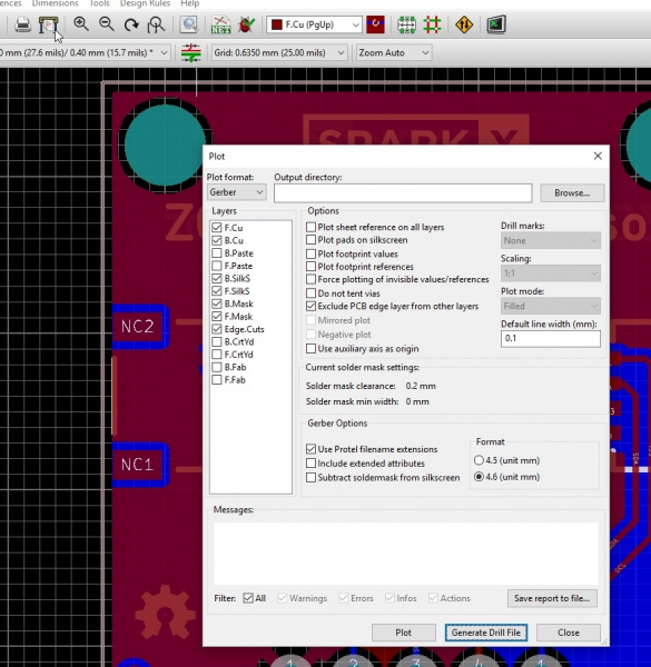
Click on the 'Plot' button next to the printer icon in the top bar to open the 'Plot' window.
In general, there are 8x layers you need to have a PCB fabricated:
- Top Copper (F.Cu)+ Soldermask (F.Mask) + Silkscreen (F.SilkS)
- Bottom Copper (B.Cu) + Soldermask (B.Mask) + Silkscreen (B.SilkS)
- Board outline (Edge.Cuts)
- Drill file
In the Plot window with the Plot format set for Gerber, be sure these Layers are checked:
- ☑ F.Cu
- ☑ B.Cu
- ☑ B.SilkS
- ☑ F.SilkS
- ☑ B.Mask
- ☑ F.Mask
- ☑ Edge.Cuts
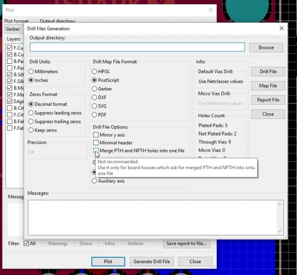
Additionally, click on 'Generate Drill File' button. You can use the defaults here as well. More on the PTH vs. NPTH check box in a minute. For now just click 'Drill File' or press enter to generate the drill file.
Click on 'Close' in the 'Drill Files Generation' window.
Click 'Plot' to generate the gerber files for the layers and then click 'Close'.
Time to Review Your Gerbers
This is the last chance to catch any errors before paying real money. Reviewing the gerber layers often shows you potential errors or problems before you send them off to fab.
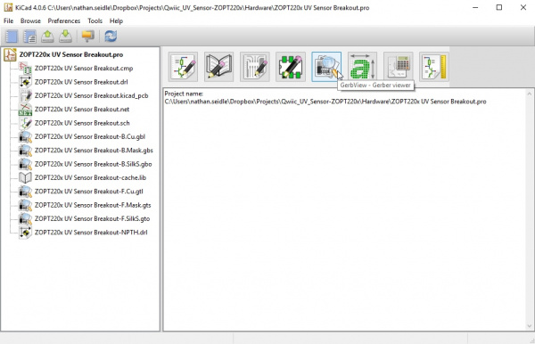
Return to the main KiCad project window and open up GerbView by clicking on the button.
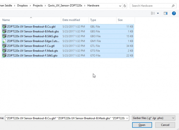
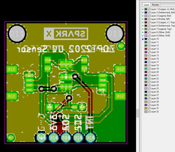
Once KiCad's GerbView is open, click on File -> Load Gerber File. Select all the files shown and click Open.
Next, click File -> Load EXCELLON Drill File. Load your drill files by selecting the all the drill files shown and click 'Open'. They should be in the same directory.
The layout looks very different but this is a good thing. You've been staring at your design for hours and it's hard for your brain to see issues. I generally do not change the layer colors unless I have to. I want the gerber review to be jarring and different from my layout practices so that I'm more likely to catch issues.
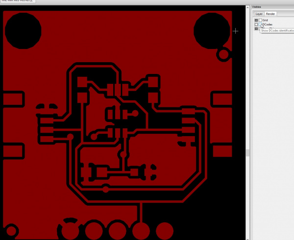
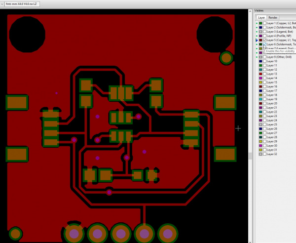
From this view, turn off all the layers but the Top Copper (layer 5). Additionally from the Render menu, turn off the Grid and DCodes. This will make the review less cluttered.
Now step through the different layers by toggling them on and off. You're looking for irregularities and things that look out of place. Here are some things I look for:
- Do any traces have weird routing that could be improved?
- Do the vias line up with the top copper where they should?
- Does the top solder mask make sense with the SMD IC's footprint?
- Are the via's covered in soldermask (also called 'tented vias') or are they exposed?
- Does the top silkscreen look good? Make sense? Everything aligned the way I want it? Are pin 1 indicators clear?
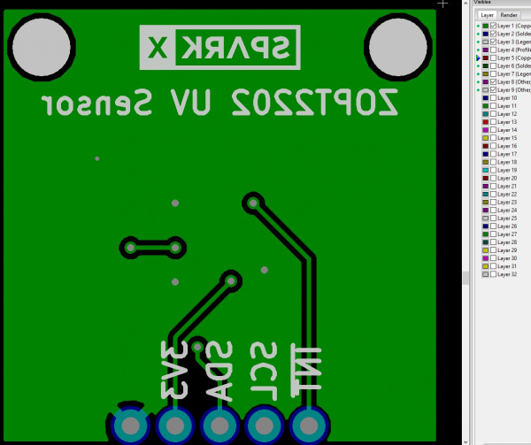
Now turn everything off and repeat for the bottom layers.
Did you catch it? There are a handful of things wrong with this example.
- The bottom silkscreen is missing the GND indicator.
- The top GND silkscreen indicator is in italics.
- There are two drill files for some reason.
Leaving a silkscreen indicator off won't break your board but it's small defects like this that the gerber review is meant to catch.
Homework:
Take a moment and return to the PCB layout window to edit the make these corrections.
- Add the a silkscreen to the bottom layer for GND. To do this, select the bottom silk layer (B.SilkS) in Pcbnew. Click on Place -> Text, type "GND" in the Text: field, and click 'OK'. You can also copy text on the bottom silkscreen layer by right clicking it, selecting Duplicate, and placing text next to the GND pad. Make sure to change text to GND by right clicking the text, selecting Properties, changing the text, and clicking 'OK'.
- Change the top GND indicator so it's not italics. To do this, edit the text properties and change the Style: to Normal.
- Plot new gerber files.
- Review your work in GerbView to verify the fixes.
Now, we need to deal with the two drill files.
PTH vs NPTH
When generating the drill file for this design two files where generated:
- *.drl - The standard EXCELLON drill file you need to send to PCB fab house.
- *-NPTH.drl - The non-plated through hole drill file.
Non-plated through holes are holes on your PCB that do not have copper covering the vertical walls of the hole. This is sometimes required for advanced designs where thorough electrical isolation is needed. However, it is rare. While plated through holes (PTH) are common and cheap, NPTH requires an extra step in the PCB fabrication process and will often cost extra.
We don't need NPTH for this design, so what happened? The 'STAND-OFF' footprint (i.e. used for the drill holes top of the board for mounting holes) was imported from the SparkFun Eagle library and KiCad seems to think it is a non-plated hole for some reason.
To correct this go back to the PCB layout, click on the Plotter, click 'Generate Drill File' and select the box that says 'Merge PTH and NPTH holes into one file'. In a later section, we'll go over how to edit the 'STAND-OFF' footprint to use a regular PTH hole.
Solder Paste Stencils
Are you doing SMD reflow? Need to order a stencil to apply the solder paste to your board? Turn on F.Paste in the Plot window to generate the top paste layer.
This *.gtp file is sent to a stencil fabricator to create the stainless steel or mylar solder paste stencil. If you're unfamiliar with stenciling solder paste we have a fabulous tutorial.
We use OSHStencils for our proto stencils. The top paste layer is not needed to fabricate a PCB.
Order Your Board!
If you're happy with your layout, let's order some PCBs! Every fab house understand and works with gerber files, so navigate to the directory on your computer where your KiCad project resides.
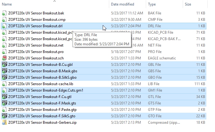
Select and zip the following 8x files:
- *.drl - Drill file
- *.gbl - Gerber Bottom Layer
- *.gbs - Gerber Bottom Soldermask
- *.gbo - Gerber Bottom Silkscreen (Overlay)
- *.Edge.Cuts.gm1 - Board Outline (Gerber Mechanical 1)
- *.gtl - Gerber Top Layer
- *.gts - Gerber Top Soldermask
- *.gto - Gerber Top Silkscreen (Overlay)
You could zip all the files in the directory and send them off to your fab house but I don't recommend it. There are a tremendous number of PCB layout software packages generating all sorts of different file names and formats. It's often difficult to tell if ** *.cmp ** is a gerber file or something else. Does the customer care about the ***.gtp** file or is that just extra? It's better to give the fab house only what you want fabricated.
The final step? Order your boards! The gerbers are the universal way to communicate with a PCB vendor. There are hundreds if not thousands of PCB vendors out there. Shop around!
In addition to your gerbers, you'll need to specify via email or the PCB vendor's website various elements of the PCB:
- What thickness PCB? 1.6mm is standard but 0.8mm is just as rigid and may help with 50 ohm trace impedance matching.
- What color soldermask? Green is default but red looks awesome.
- What color silkscreen? White is most common but other colors are available.
- How many layers? This example is a 2x layer board meaning there is just a top copper and bottom copper. However, some designs need to have 4x, 10x, and even 16x layers to route the board. Additional layers increase the cost significantly.
The Soldermask Looks Big
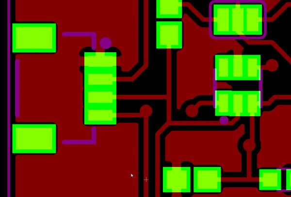
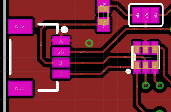
If you had a look at the soldermask on this PCB and wondered why it looked odd, you're not alone. Let's compare the PCB's soldermask for KiCad (as shown in green) and Eagle (as shown in pink). You should notice two things:
- In the KiCad design, I have a pad on the main sensor that looks like it's slightly mis-placed. Pad 1 doesn't line up with the other pads. Weird. It's a problem that needs to be fixed, but the error won't kill the board.
- More importantly, the soldermask on the Eagle design has gaps between the pins on the connector and the sensor IC. This will help reduce solder bridging between pins. In the KiCad version, the mask apertures look too big.
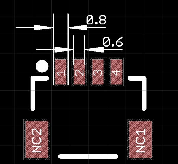
In the image below, we can see the SMD Qwiic connector within Eagle. The default soldermask clearance is 0.1mm per side in Eagle.
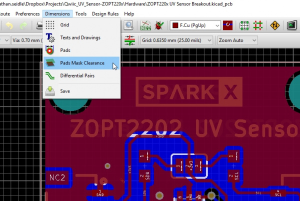
In KiCad's Pcbnew, open the ZOPT220x Breakout and click on Dimensions -> Pads Mask Clearance. KiCad's solder mask clearance has a default of 0.2mm per side. We recommend you change this value to 0.1mm. Most fab houses will use 0.1mm as their default as well. You will then need to re-export your gerbers and load them back into GerbView.
Making the clearance smaller than 0.1mm will cause difficulties for the fab house to get the registration correct.
