Beginner's Guide to KiCad
 Nate
Nate 
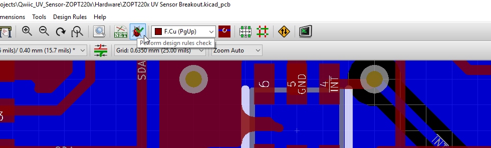
Running Design Rule Check
Click on the ladybug with the green check mark on it to open the Design Rule Check (DRC) window.
Let's take a moment to talk trace width, trace spacing, and vias. In general, SparkFun designs boards with:
- 10mil trace width
- 10mil trace spacing
- 20mil vias
We go smaller than this on many designs but if you're designing your first PCB, do not design it with 4mil traces and 8mil vias. You shouldn't need to go that small on your first board.
Why design in 10mil trace/space when a fab house allows 8mil or smaller for the same price?
Making PCBs is tricky and for each increment of tolerance you remove you increase the chances that the PCB (proto or not) will be fabricated with an error. And those errors can be hard to identify. We design with 10mil trace/space in order to insure and reduce the probability that we'll see PCBs with errors on the production floor. There's nothing worse than troubleshooting a faulty product and asking yourself: "I've tried every rework and soldering trick in the book, is it the PCB that's bad?"
That stated, we are seeing many PCB fab houses charge low prices for 7mil trace/space and 12mil vias. If you've got a complex board with tight layout challenges, it's better use the smaller trace/space and vias. Save yourself the layout time and rely on the PCB fab house to correctly fabricate your board.
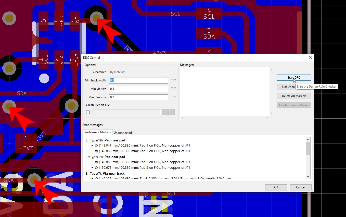
We generally use the KiCad defaults of:
- Clearance: By Netclass
- Min Track Width: 0.2mm = 7.9mil
- Min Via Size: 0.4mm = 15.7mil
Press enter again to run the DRC with the default settings.
ErrType(): Via near track
Aw shucks! What's wrong with my board? The vias marked with red arrows are too close to the traces near by. The error message will show up in the window as an error indicating: "Via near track." Fix them by ripping up (press 'Delete') any traces near the vias and re-route them (press 'x').
After adjusting the traces causing the issues, re-run the DRC. These three flags should disappear.
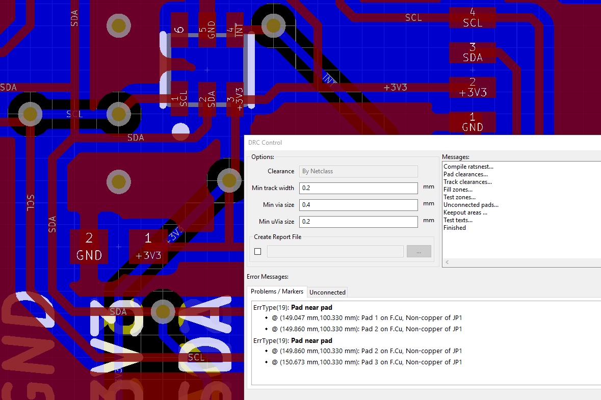
Congrats! You've fixed those "Via near track" issues.
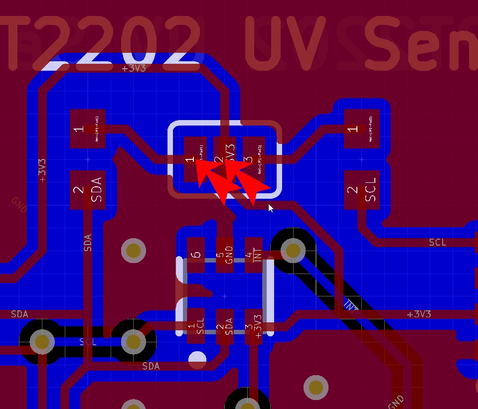
ErrType(): Pad near pad
But wait, we are not done yet! There are still two DRC error arrows left with the error indicating: "Pad near pad". KiCad is trying to tell us the pads on this solder jumper are too close together. SparkFun has used this footprint for years and is comfortable with the design so let's change the Netclass clearance constraint.
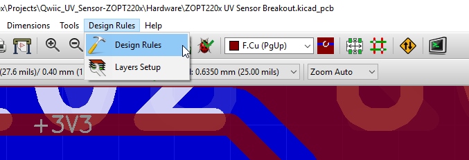
Open the DRC rules from the Design Rules menu.
Here is where you can create specific rules for specific traces and classes of traces. The problem that we are running into is the Default Clearance is 7.9mil (0.2mm). If we decrease this to 7mil (0.1778mm), click 'OK', and re-run the DRC...
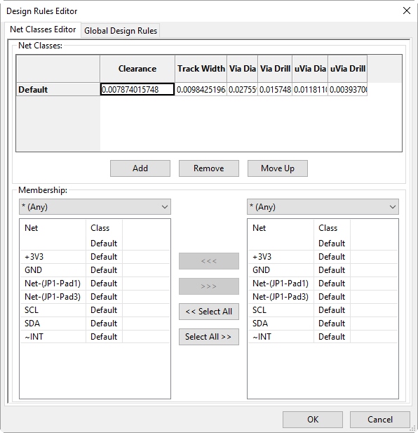
DRC errors resolved! Now reducing the DRC clearances in order to get your board to pass DRC is not an ideal solution. We want the pads on the solder jumper to be close enough to be easily jumpered with solder so increasing the distance between the pads on the footprint would be counterproductive. In general, you should set your DRC rules and stick to them.

Watch Your Airwires!
One last note about DRC: Leaving airwires on your PCB is a sure fire way to generate coasters (bad, unusable PCBs).

From the DRC window there is a 'List Unconnected' button. This will show you the location of any unconnected traces (I had to rip up the SDA trace on the bottom right side of the PCB to show this error). It's very important that you check for airwires before ordering your PCBs. As you progress through your layout, I recommend focusing on the 'Unconnected' count at the bottom of the screen (circled in pink). If you think you are done routing a board but still show a few unconnected wires that you can't find, the DRC window will help you locate them.
Press 'ctrl+s' to save your work.
Well done. You've made it through design rule checking! Now it's time to order boards.