PCB Basics
 SFUptownMaker
 Overview
One of the key concepts in electronics is the printed circuit board or PCB. It's so fundamental that people often forget to explain what a PCB is. This tutorial will breakdown what makes up a PCB and some of the common terms used in the PCB world.
Over the next few pages, we'll discuss the composition of a printed circuit board, cover some terminology, a look at methods of assembly, and discuss briefly the design process behind creating a new PCB.
Suggested Reading
Before you get started you may want to read up on some concepts we build upon in this tutorial:
- What is Electricity?
- What is a Circuit?
- Voltage, Current, Resistance, and Ohm's Law
- Connector Basics
- Soldering 101 - PTH
- Signals
Translations
Minh Tuấn was kind enough to translate this tutorial to Vietnamese. You can view the translation here.
What's a PCB?
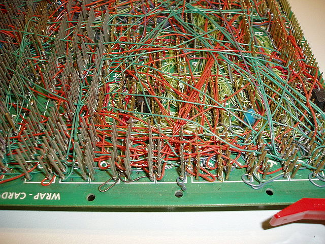
Printed circuit board is the most common name but may also be called "printed wiring boards" or "printed wiring cards". Before the advent of the PCB circuits were constructed through a laborious process of point-to-point wiring. This led to frequent failures at wire junctions and short circuits when wire insulation began to age and crack.
-> 
courtesy Wikipedia user Wikinaut <-
A significant advance was the development of wire wrapping, where a small gauge wire is literally wrapped around a post at each connection point, creating a gas-tight connection which is highly durable and easily changeable.
As electronics moved from vacuum tubes and relays to silicon and integrated circuits, the size and cost of electronic components began to decrease. Electronics became more prevalent in consumer goods, and the pressure to reduce the size and manufacturing costs of electronic products drove manufacturers to look for better solutions. Thus was born the PCB.
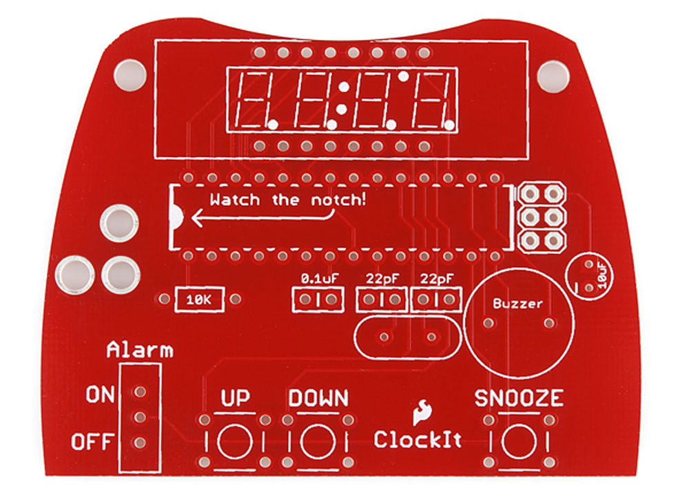
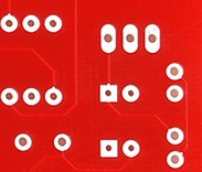
PCB is an acronym for printed circuit board. It is a board that has lines and pads that connect various points together. In the picture above, there are traces that electrically connect the various connectors and components to each other. A PCB allows signals and power to be routed between physical devices. Solder is the metal that makes the electrical connections between the surface of the PCB and the electronic components. Being metal, solder also serves as a strong mechanical adhesive.
Composition
A PCB is sort of like a layer cake or lasagna- there are alternating layers of different materials which are laminated together with heat and adhesive such that the result is a single object.
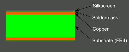
Let's start in the middle and work our way out.
FR4
The base material, or substrate, is usually fiberglass. Historically, the most common designator for this fiberglass is "FR4". This solid core gives the PCB its rigidity and thickness. There are also flexible PCBs built on flexible high-temperature plastic (Kapton or the equivalent).
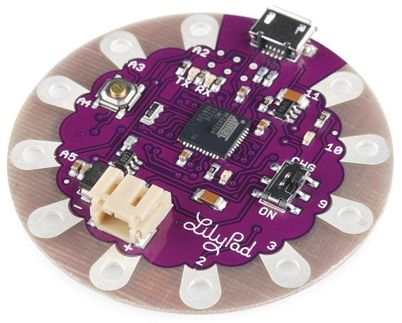
You will find many different thickness PCBs; the most common thickness for SparkFun products is 1.6mm (0.063"). Some of our products- LilyPad boards and Arudino Pro Micro boards- use a 0.8mm thick board.
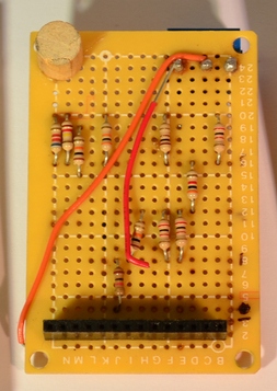
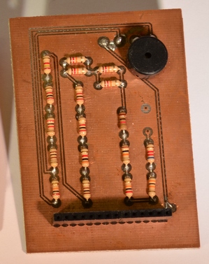
Cheaper PCBs and perf boards (shown above) will be made with other materials such as epoxies or phenolics which lack the durability of FR4 but are much less expensive. You will know you are working with this type of PCB when you solder to it - they have a very distictive bad smell. These types of substrates are also typically found in low-end consumer electronics. Phenolics have a low thermal decomposition temperature which causes them to delaminate, smoke and char when the soldering iron is held too long on the board.
Copper
The next layer is a thin copper foil, which is laminated to the board with heat and adhesive. On common, double sided PCBs, copper is applied to both sides of the substrate. In lower cost electronic gadgets the PCB may have copper on only one side. When we refer to a double sided or 2-layer board we are referring to the number of copper layers (2) in our lasagna. This can be as few as 1 layer or as many as 16 layers or more.
The copper thickness can vary and is specified by weight, in ounces per square foot. The vast majority of PCBs have 1 ounce of copper per square foot but some PCBs that handle very high power may use 2 or 3 ounce copper. Each ounce per square translates to about 35 micrometers or 1.4 thousandths of an inch of thickness of copper.
Soldermask
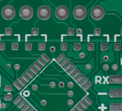
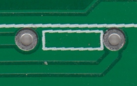
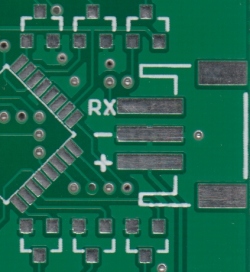
The layer on top of the copper foil is called the soldermask layer. This layer gives the PCB its green (or, at SparkFun, red) color. It is overlaid onto the copper layer to insulate the copper traces from accidental contact with other metal, solder, or conductive bits. This layer helps the user to solder to the correct places and prevent solder jumpers.
In the example below, the green solder mask is applied to the majority of the PCB, covering up the small traces but leaving the silver rings and SMD pads exposed so they can be soldered to.
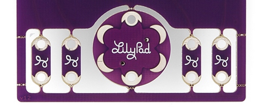
Soldermask is most commonly green in color but nearly any color is possible. We use red for almost all the SparkFun boards, white for the IOIO board, and purple for the LilyPad boards.
Silkscreen
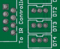
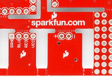
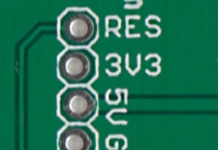
The white silkscreen layer is applied on top of the soldermask layer. The silkscreen adds letters, numbers, and symbols to the PCB that allow for easier assembly and indicators for humans to better understand the board. We often use silkscreen labels to indicate what the function of each pin or LED.
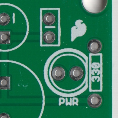
Silkscreen is most commonly white but any ink color can be used. Black, gray, red, and even yellow silkscreen colors are widely available; it is, however, uncommon to see more than one color on a single board.
Terminology
Now that you've got an idea of what a PCB structure is, let's define some terms that you may hear when dealing with PCBs:
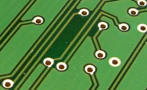
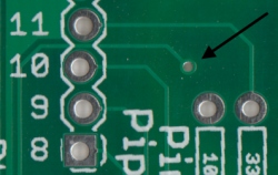
- Annular ring - the ring of copper around a plated through hole in a PCB.
- DRC - design rule check. A software check of your design to make sure the design does not contain errors such as traces that incorrectly touch, traces too skinny, or drill holes that are too small.
- Drill hit - places on a design where a hole should be drilled, or where they actually were drilled on the board. Inaccurate drill hits caused by dull bits are a common manufacturing issue.
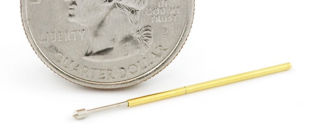
- Finger - exposed metal pads along the edge of a board, used to create a connection between two circuit boards. Common examples are along the edges of computer expansion or memory boards and older cartridge-based video games.
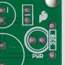
- Mouse bites - an alternative to v-score for separating boards from panels. A number of drill hits are clustered close together, creating a weak spot where the board can be broken easily after the fact. See the SparkFun Protosnap boards for a good example.
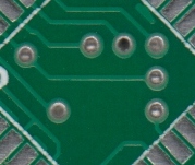
- Pad - a portion of exposed metal on the surface of a board to which a component is soldered.
- Panel - a larger circuit board composed of many smaller boards which will be broken apart before use. Automated circuit board handling equipment frequently has trouble with smaller boards, and by aggregating several boards together at once, the process can be sped up significantly.
- Paste stencil - a thin, metal (or sometimes plastic) stencil which lies over the board, allowing solder paste to be deposited in specific areas during assembly.
- Pick-and-place - the machine or process by which components are placed on a circuit board.
- Plane - a continuous block of copper on a circuit board, define by borders rather than by a path. Also commonly called a "pour".
- Plated through hole - a hole on a board which has an annular ring and which is plated all the way through the board. May be a connection point for a through hole component, a via to pass a signal through, or a mounting hole.
- Pogo pin - spring-loaded contact used to make a temporary connection for test or programming purposes.
- Reflow - melting the solder to create joints between pads and component leads.
- Silkscreen - the letters, number, symbols, and imagery on a circuit board. Usually only one color is available, and resolution is usually fairly low.
- Slot - any hole in a board which is not round. Slots may or may not be plated. Slots sometimes add to add cost to the board because they require extra cut-out time.
- Solder paste - small balls of solder suspended in a gel medium which, with the aid of a paste stencil, are applied to the surface mount pads on a PCB before the components are placed. During reflow, the solder in the paste melts, creating electrical and mechanical joints between the pads and the component.
- Solder pot - a pot used to quickly hand solder boards with through hole components. Usually contains a small amount of molten solder into which the board is quickly dipped, leaving solder joints on all exposed pads.
- Soldermask - a layer of protective material laid over the metal to prevent short circuits, corrosion, and other problems. Frequently green, although other colors (SparkFun red, Arduino blue, or Apple black) are possible. Occasionally referred to as "resist".
- Solder jumper - a small, blob of solder connecting two adjacent pins on a component on a circuit board. Depending on the design, a solder jumper can be used to connect two pads or pins together. It can also cause unwanted shorts.
- Surface mount - construction method which allows components to be simply set on a board, not requiring that leads pass through holes in the board. This is the dominant method of assembly in use today, and allows boards to be populated quickly and easily.
- Thermal - a small trace used to connect a pad to a plane. If a pad is not thermally relieved, it becomes difficult to get the pad to a high enough temperature to create a good solder joint. An improperly thermally relieved pad will feel "sticky" when you attempt to solder to it, and will take an abnormally long time to reflow.
- Thieving - hatching, gridlines, or dots of copper left in areas of a board where no plane or traces exist. Reduces difficulty of etching because less time in the bath is required to remove unneeded copper.
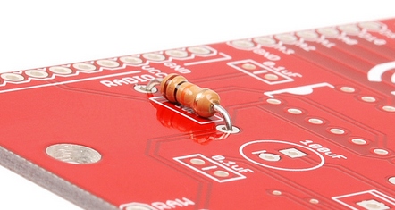
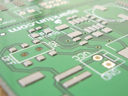
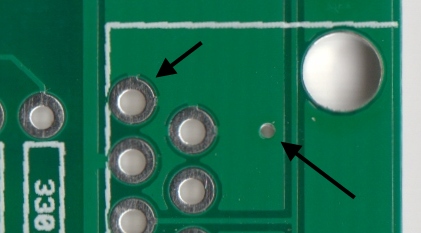
- Trace - a continuous path of copper on a circuit board.
-> A small trace connecting the Reset pad to elsewhere on the board. A larger, thicker trace connects to the 5V power pin. <-
- V-score- a partial cut through a board, allowing the board to be easily snapped along a line.
- Via - a hole in a board used to pass a signal from one layer to another. Tented vias are covered by soldermask to protect them from being soldered to. Vias where connectors and components are to be attached are often untented (uncovered) so that they can be easily soldered.
- Wave solder - a method of soldering used on boards with through-hole components where the board is passed over a standing wave of molten solder, which adheres to exposed pads and component leads.
Designing Your Own!
How do you go about designing your own PCB? The ins and outs of PCB design are way too in depth to get into here, but if you really want to get started, here are some pointers:
- Find a CAD package: there are a lot of low-cost or free options out there on the market for PCB design. Things to consider when choosing a package:
- Community support: are there a lot of people using the package? The more people using it, the more likely you are to find ready-made libraries with the parts you need.
- Ease-of-use: if it's painful to use it, you won't.
- Capability: some programs place limitations on your design- number of layers, number of components, size of board, etc. Most of them allow you to pay for a license to upgrade their capability.
- Portability: some free programs do not allow you to export or convert your designs, locking you in to one supplier only. Maybe that's a fair price to pay for convenience and price, maybe not.
- Look at other people's layouts to see what they have done. Open Source Hardware makes this easier than ever.
- Practice, practice, practice.
- Maintain low expectations. Your first board design will have lots of problems. Your 20th board design will have fewer, but will still have some. You'll never get rid of them all.
- Schematics are important. Trying to design a board without a good schematic in place first is an exercise in futility.
Finally, a few words on the utility of designing your own circuit boards. If you plan on making more than one or two of a given project, the payback on designing a board is pretty good- point-to-point wiring circuits on a protoboard is a hassle, and they tend to be less robust than purpose-designed boards. It also allows you to sell your design if it turns out to be popular.
Resources and Going Further
Interested in learning more foundational topics?
See our Engineering Essentials page for a full list of cornerstone topics surrounding electrical engineering.
PCBs are just the beginning! From here we recommend you explore:
- Soldering 101 - PTH
- How to Read a Schematic
- How to install and setup Eagle PCB software
- How to layout PTH PCBs: Schematic
- How to layout PTH PCBs: Board Layout
- Creating SMD Footprints
- Creating SMD PCBs
- T³: Etching Your Own Circuit Boards
- Electronics Assembly
If you'd like to share your PCB creations with the world, check out these tutorials: