Using EAGLE: Schematic
 jimblom
 Introduction
PCB design in EAGLE is a two-step process. First you design your schematic, then you lay out a PCB based on that schematic. EAGLE's board and schematic editors work hand-in-hand. A well-designed schematic is critical to the overall PCB design process. It will help you catch errors before the board is fabricated, and it'll help you debug a board when something doesn't work.
This tutorial is the first of a two-part Using EAGLE series, and it's devoted entirely to the schematic-designing side of EAGLE. In part 2, Using EAGLE: Board Layout, we'll use the schematic designed in this tutorial as the basis for our example board layout.
Suggested Reading
If you'd like to follow along with this tutorial, make sure you've installed and setup the EAGLE software. Our How to Install and Setup EAGLE tutorial goes over this process step-by-step, and it also covers the basics of what EAGLE is and what makes it great. It also covers how to download and install the SparkFun EAGLE libraries we'll be using in this tutorial. Definitely read through that tutorial before you continue on.
We'd also recommend you read and understand the concepts behind these tutorials:
Create a Project
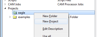
We'll start by making a new project folder for our design. In the control panel, under the "Projects" tree, right click on the directory where you want the project to live (by default EAGLE creates an "eagle" directory in your home folder), and select "New Project".
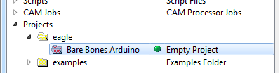
Give the newly created, red project folder a descriptive name. How about "Bare Bones Arduino".
Project folders are like any regular file system folder, except they contain a file named "eagle.epf". The EPF file links your schematic and board design together, and also stores any settings you may have set especially for the project.
Create a Schematic
The project folder will house both our schematic and board design files (and eventually our gerber files too). To begin the design process, we need to lay out a schematic.
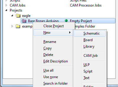
To add a schematic to a project folder, right-click the folder, hover over "New" and select "Schematic".
A new, blank window should immediately pop up. Welcome to the schematic editor!
Adding Parts to a Schematic
Schematic design is a two step process. First you have to add all of the parts to the schematic sheet, then those parts need to be wired together. You can intermix the steps -- add a few parts, wire a few parts, then add some more -- but since we already have a reference design we'll just add everything in one swoop.
Using the ADD Tool
The ADD tool --  (on the left toolbar, or under the Edit menu) -- is what you'll use to place every single component on the schematic. The ADD tool opens up a library navigator, where you can expand specific libraries and look at the parts it holds. With a part selected on the left side, the view on the right half should update to show both the schematic symbol of the part and its package.
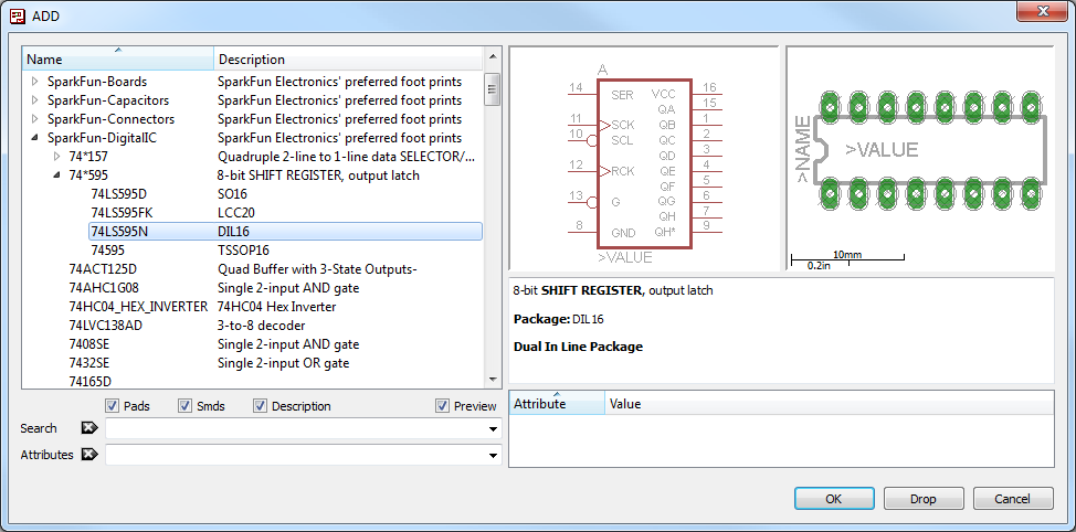
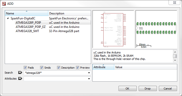
The ADD tool also has search functionality -- very helpful when you have to navigate through dozens of libraries to find a part. The search is very literal, so don't misspell stuff! You can add wildcards to your search by placing an asterisk (*) before and/or after your search term. For example if you search for atmega328 you should find a single part/package combo in the SparkFun-DigitalIC library, but if you search *atmega328* (note asterisks before and after), you'll discover two more versions of the IC (because they're actually named "ATMEGA328P"). You'll probably want to get accustomed to always adding an asterisk before and after your search term.
To actually add a part from a library either select the part you want and click "OK", or double-click your part.
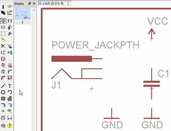
Step 1: Add a Frame
The frame isn't a critical component for what will be the final PCB layout, but it keeps your schematic looking clean and organized. The frame we want should be in the SparkFun-Aesthetics library, and it's named FRAME-LETTER. Find that by either searching or navigating and add it to your schematic.
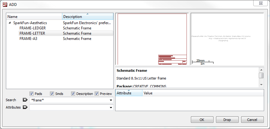
After selecting the part you want to add, it'll "glow" and start hovering around following your mouse cursor. To place the part, left-click (once!). Let's place the frame so its bottom-left corner runs right over our origin (the small dotted cross, in a static spot on the schematic).

After placing a part, the add tool will assume you want to add another -- a new frame should start following your cursor. To get out of the add-mode either hit escape (ESC) twice or just select a different tool.
Step 2: Save (And Save Often)
Right now your schematic is an untitled temporary file living in your computer's ether. To save either go to File > Save, or just click the blue floppy disk icon --  . Name your schematic something descriptive. How about "BareBonesArduino.sch" (SCH is the file format for all EAGLE schematics).
As a bonus, after saving, your frame's title should update accordingly (you may have to move around the screen, or go to View > Redraw).
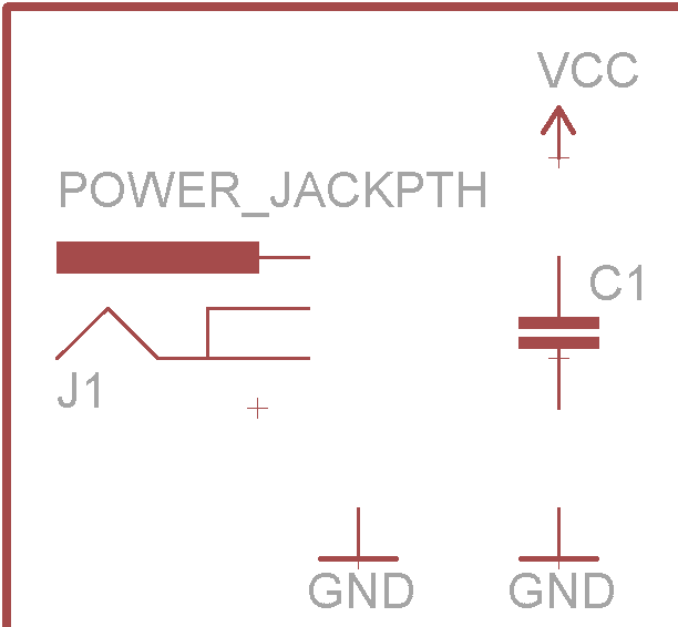
Step 3: Adding the Power Input
Next we'll add four different parts all devoted to our voltage supply input. Use the add tool for these parts:
| Part Description | Library | Part Name | Quantity |
|---|---|---|---|
| 5.5mm Barrel Jack (PTH) | SparkFun-Connectors | POWER_JACKPTH | 1 |
| 0.1µF Ceramic Capacitor | SparkFun-Capacitors | CAPPTH | 1 |
| Voltage Supply Symbol | SparkFun-Aesthetics | VCC | 1 |
| Ground Symbol | SparkFun-Aesthetics | GND | 2 |
All of these parts will go in the top-left of the schematic frame. Arranged like this:
If you need to move parts around, use the MOVE tool --  (left toolbar or under the Edit menu). Left-click once on a part to pick it up (your mouse should be hovering over the part's red "+" origin). Then left click again when it's where it needs to be.
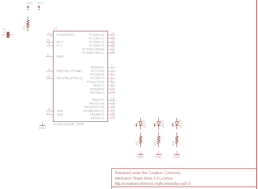
Step 4: Microprocessor and Supporting Circuitry
Next we'll add the main component of the design -- the ATmega328 microprocessor -- as well as some components to support it. Here are the parts we'll add:
| Part Description | Library | Exact Part Name | Quantity |
|---|---|---|---|
| ATmega328P (PTH) | SparkFun-DigitalIC | ATMEGA328P_PDIP | 1 |
| ¼W Resistors | SparkFun-Resistors | RESISTORPTH-1/4W | 4 |
| 5mm LEDs | SparkFun-LED | LED5MM | 3 |
| 0.1µF Ceramic Capacitor | SparkFun-Capacitors | CAPPTH | 1 |
| Voltage Supply Symbol | SparkFun-Aesthetics | VCC | 2 |
| Ground Symbol | SparkFun-Aesthetics | GND | 4 |
To rotate parts as your placing them, either select one of the four options on the rotate toolbar --  -- or right click before placing the part. Place your microcontroller in the center of the frame, then add the other parts around it like so:
Step 5: Adding the Connectors
Three connectors will finish off our design. One 8-pin connector to break out the analog pins, a 6-pin serial programming header, and a 2x3-pin ICSP programming header. Here are the three parts to add for this step:
| Part Description | Library | Exact Part Name | Quantity |
|---|---|---|---|
| 8-Pin 0.1" Header | SparkFun-Connectors | M081X08 | 1 |
| 2x3 AVR Programming Header | SparkFun-Connectors | AVR_SPI_PRG_6PTH | 1 |
| 6-Pin Serial Programming Header | SparkFun-Connectors | ARDUINO_SERIAL_PROGRAMPTH | 1 |
| Voltage Supply Symbol | SparkFun-Aesthetics | VCC | 2 |
| Ground Symbol | SparkFun-Aesthetics | GND | 2 |
Finally! Here's what your schematic should look like with every part added:
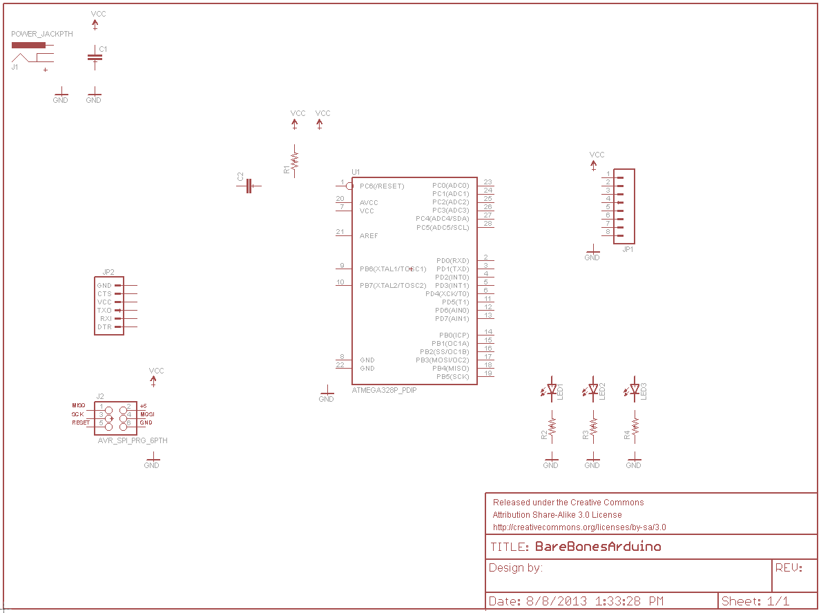
Next we'll wire net them all together.
Wiring Up the Schematic
With all of the parts added to our schematic, it's time to wire them together. There's one major caveat here before we start: even though we're wiring parts on the schematic, we not going to use the WIRE tool --  -- to connect them together. Instead, we'll use the NET tool --
  (left toolbar, or under the Draw menu). The WIRE tool would be better-named as a line-drawing tool, NET does a better job of connecting components.

Using the NET Tool
To use the NET tool, hover over the very end of a pin (as close as possible, zoom in if you have to), and left-click once to start a wire. Now a green line should be following your mouse cursor around. To terminate the net, left-click on either another pin or a net.
The hard part, sometimes, is identifying which part on a circuit symbol is actually a pin. Usually they're recognizable by a thin, horizontal, red line off to the side of a part. Sometimes (not always) they're labeled with a pin number. Make sure you click on the very end of the pin when you start or finish a net route.
Route the Power Input Circuit
Start back in the upper left, and route the power input circuit like so:
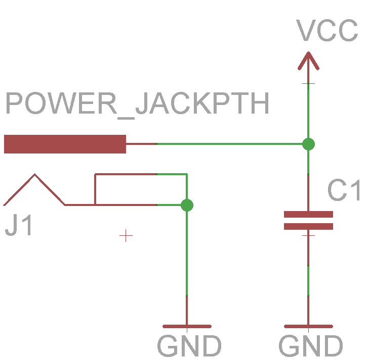
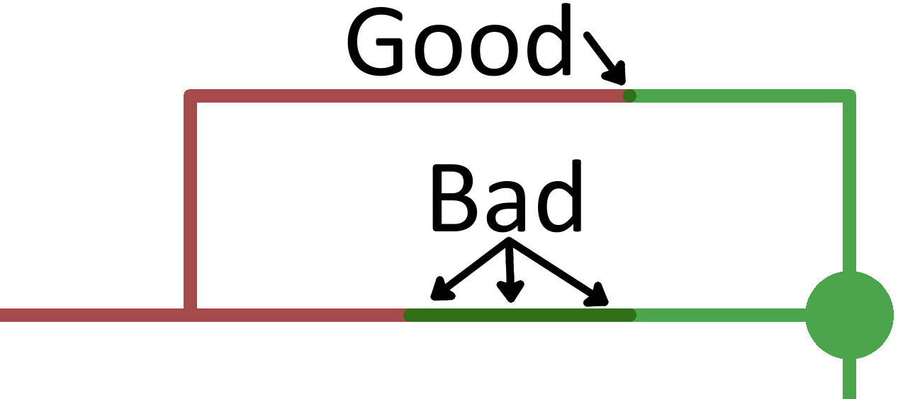
Whenever a net splits in two directions a junction node is created. This signifies that all three intersecting nets are connected. If two nets cross, but there's not a junction, those nets are not connected.
Route the ATmega328 Circuit
Next we'll route the ATmega328 to its supporting circuitry. There's LEDs, a connector, resistor, capacitor and VCC/GND symbols to route to:
Don't forget to add nets between the LEDs, resistors, and GND symbols!
Making Named, Labeled Net Stubs
The remaining nets we have to make are not going to be as easy to cleanly route. For example, we need to connect the TXO pin on JP2 to the ATmega's RXD pin, all the way on the other side. You could do it, it would work, but it'd be really ugly. Instead, we'll make net "stubs" and give them unique names to connect them.
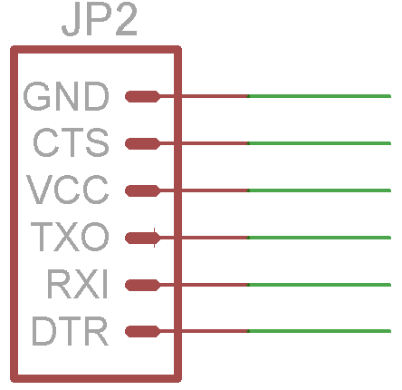
We'll start by adding short, one-sided nets to each of the six pins on the serial connector. Begin by starting a net at a pin, just as you've been doing. Terminate the net by left-clicking a few grid-lengths over to the right of the pin. Then, instead of routing to another pin, just hit ESC to finish the route. When you're done, it should look like this:
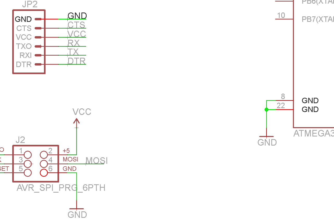
Next, we'll use the NAME tool --  (left toolbar, or under the Edit menu) -- to name each of the six nets. With the NAME tool selected, clicking on a net should open a new dialog. Start by naming the net connected to the top, GND pin. Delete the auto-generated name (e.g. N$14), and replace it with "GND" (sans the quotation marks). This should result in a warning dialog, asking you if you want to connect this net to all of the other nets named "GND" (that would be every net connected to a GND symbol). Thanks for looking out for us EAGLE, but in this case Yes we do want to connect GND to GND.
After naming a net, you should use the LABEL tool --  -- to add a text label. With the LABEL tool selected, left-click on the net you just named. This should spawn a piece of text that says "GND", left-click again to place the label down right on top of your net.
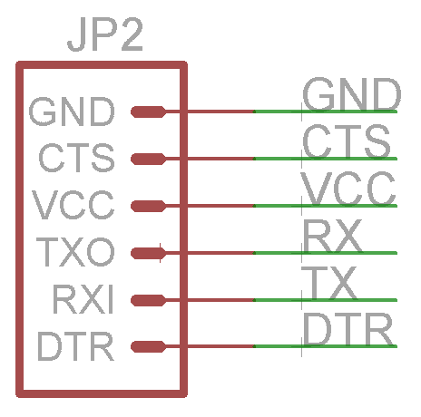
Follow that same order of operations for the remaining five net stubs. In the end, they should look like this (note the net connected to the TXO pin is named "RX", and a "TX" net connects to RXI -- that's on purpose):
VCC should be the only other net that warns you that you'll be connecting to other nets named "VCC" (anything connected to a VCC voltage node). For the other named nets, we'll need to create this same stub somewhere else. Where exactly? Well, we need to add a "RX" and "TX" net on the ATmega328, and a "DTR" nearby as well:
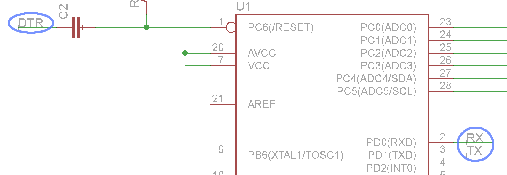
Even though there's no green net connecting these pins, every net with the same, exact name is actually connected.
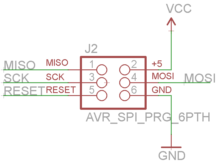
We need to do a lot of the same to connect the 2x3 programming header to the ATmega328. First, wire up the connector like so (naming/labeling MOSI, MISO, SCK, and RESET):
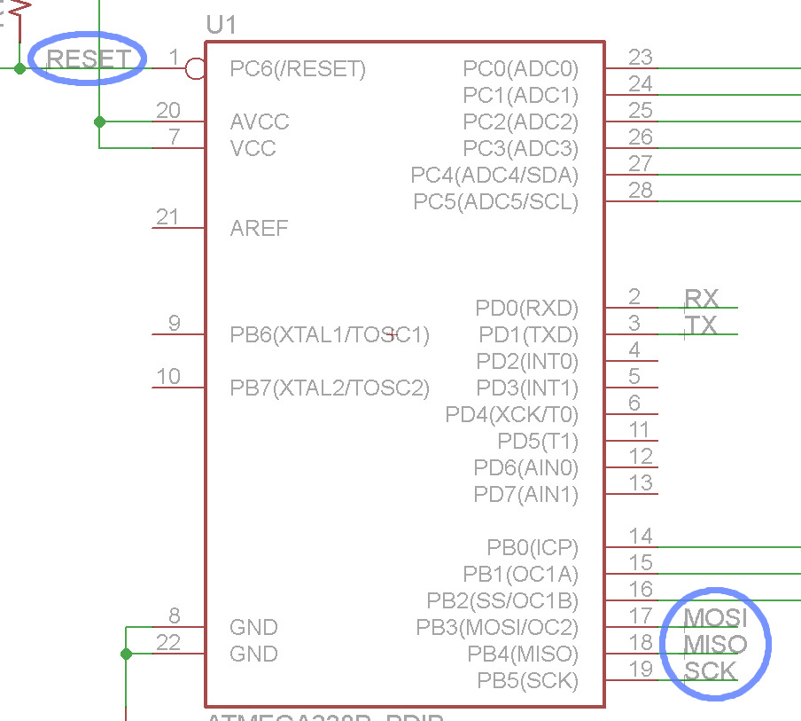
Then, back to the ATmega328, add the same four named/labeled nets:
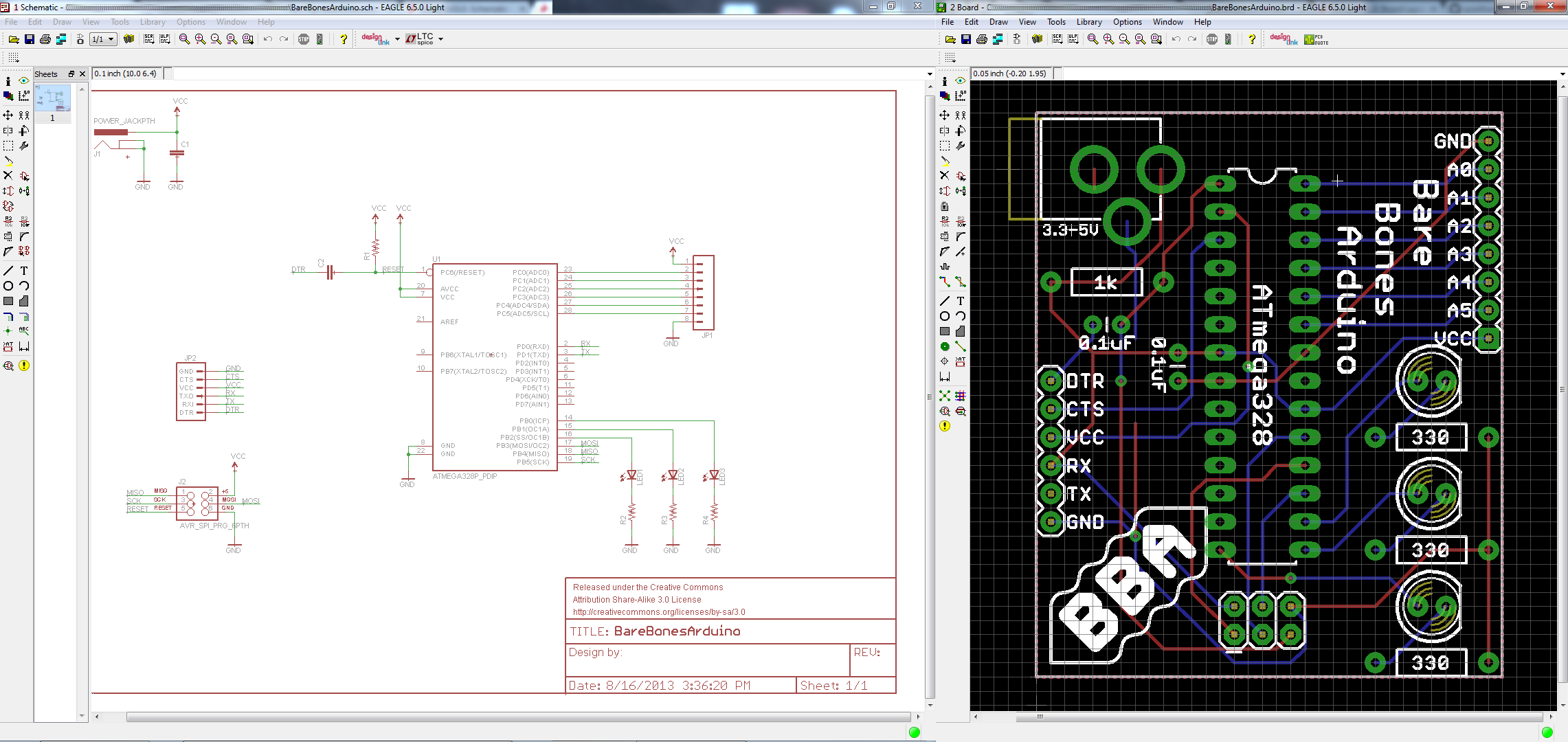
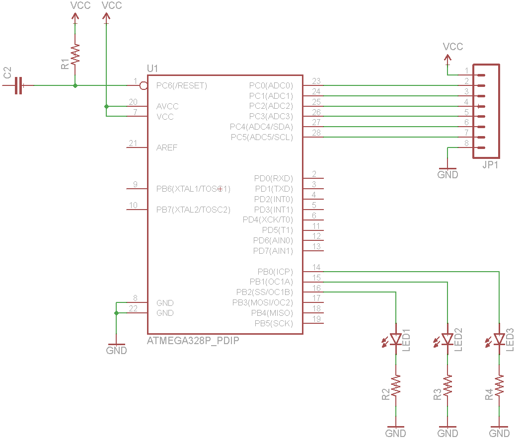
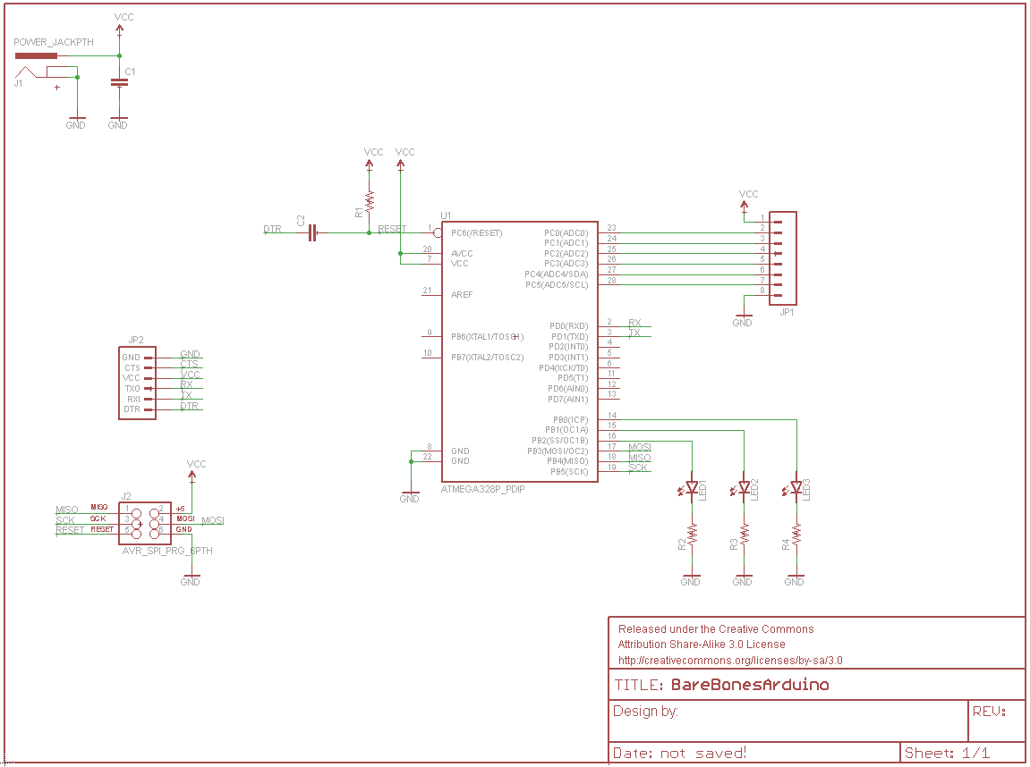
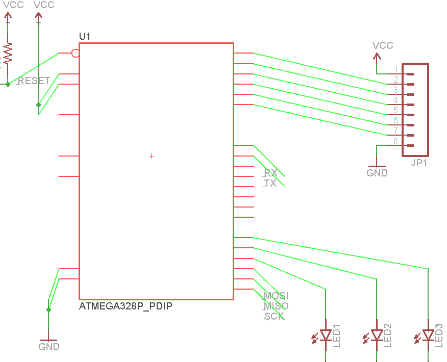
Phew -- you're done. Get excited, it's about time to lay out a PCB! When your schematic is done, it should look a little something like this:
The schematic layout is done, but there are a few tips and tricks we'd like to share before moving over to the PCB layout portion of the tutorial.
Tips and Tricks
Names and Values
Every component on your schematic should have two editable text fields: a name and a value. The name is an identifier like R1, R2, LED3, etc. Every component on the schematic should have a unique name. You can use the NAME tool -- on any component to change the name.
A part's value allows you to define unique characteristics of that part. For example, you can set a resistor's resistance, or a capacitor's capacitance. The importance of a part's value depends on what type of component it is. For parts like resistors, capacitors, inductors, etc. the value is a critical piece of information when you're generating a bill of materials or assembly sheet. To adjust a part's value parameter, use the VALUE tool --  .
.
Verifying Connections
The SHOW tool --  -- is very useful for verifying that pins across your schematic are connected correctly. If you use SHOW on a net, every pin it's connected to should light up. If you're dubious of the fact that two like-named nets are connected, give the SHOW tool a try. SHOW-ing a net connected to GND, for example, should result in a lot of GND nets lighting up.
As an alternative to show, you can temporarily MOVE a part a part to make sure nets are connected to it. Use MOVE to pick a part up, and the nets connected to it should bend and adjust to remain so. Just make sure you hit ESC to not move the part (or UNDO if you accidentally move it).
If a net isn't moving along with the part, it's not connected to the pin correctly. Double check to make sure you routed to the very end of the pin, and not a bit further:
If you have any nets incorrectly connected like above, DELETE --  -- it, and try re-netting.
Group Moving/Deleting/Etc.
Any tool that you use on a single component, can also be used on a group of them. Grouping and performing an action on that group is a two-step process. First, use the group tool --  -- to select the parts you want to modify. You can either hold down the left-mouse button and drag a box around them, or click multiple times to draw a polygon around a group. Once the group is made, every object in that group should glow.
After grouping, select the tool you want to use. The status box in the far bottom-left will have some helpful information pertaining to using the tool on a group:

In order to perform any action on a group, you have to select the tool, then hold down CTRL and right-click the group. After you CTRL+right-click, the tool will operate on the group just as it does a single component.
Copy/Paste
EAGLE's Copy --  -- and Paste --
  -- tools don't work exactly like other copy/paste tools you may have encountered before. Copy actually performs both a copy and paste when it's used. As soon as you copy a part (or any object on the schematic -- name, text, net, etc.) an exact copy will instantly spawn and follow your mouse awaiting placement. This is useful if you need to add multiples of the same part (like GND nodes or resistors).
Paste can only be used to paste a group that has previously been copied to your clipboard. To use paste you first have to create a group, then (with the copy tool selected) CTRL+right-click to copy it, but hit ESC instead of gluing it down. This'll store the copied group into your operating system's clipboard, and you can use paste to place it somewhere. This tool is especially useful if you need to copy parts of one schematic file into another.
Resources and Going Further
This tutorial is the first of a pair. The next tutorial, Using EAGLE: Board Layout, will use the schematic we designed here to lay out a "Bare Bones Arduino" PCB. If you're headed over to that tutorial next, you can get a head start by clicking the Generate/Switch to Board icon --  -- to create a board based on this schematic.
If you'd rather read about other EAGLE-related concepts, here are some tutorials you may want to check out:
- How to Create SMD PCBs -- This is a more advanced and fast-paced EAGLE tutorial. In this one, we focus on laying out a more complex, surface-mount (SMD) design.
- How to Create SMD Footprints -- If you want to create unique parts in a library, check out this tutorial.
- Making Custom Footprints in EAGLE -- Another footprint-making tutorial. This one details a unique process for making a custom 1:1 footprint.
If you'd like to share your PCB creations with the world, check out these tutorials:
Interested in learning more foundational topics?
See our Engineering Essentials page for a full list of cornerstone topics surrounding electrical engineering.
