Designing PCBs: Advanced SMD
How to Create SMD Based PCBs
This tutorial will take you through a more advanced SMD layout. It’s a marathon so get yourself a glass of wine and a mouse with a scroll wheel and then dive in.
We’re going to assume you’ve already read our other tutorials on through-hole PCB layout so you should already have Eagle and the various support files installed. We use keyboard shortcuts liberally so you better have them installed as well.
Let’s create a tool that everyone should have in their toolbox: a USB to serial converter board. The FT230X is a pretty neat USB to serial converter that should do the job nicely for us.
We’re going to assume you’re using our library that contains the FT230X. If you want to learn how to create SMD footprints for Eagle from scratch, please see this tutorial.
Suggested Reading
These are the tutorials and concepts you may want to know before starting this tutorial:
Creating the Schematic
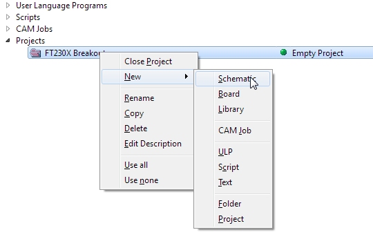
To start, create a new project in Eagle. Right click on the Projects folder and select ‘New Project’. Call the project ‘FT230X Breakout’. Right click on the folder and select New Schematic.
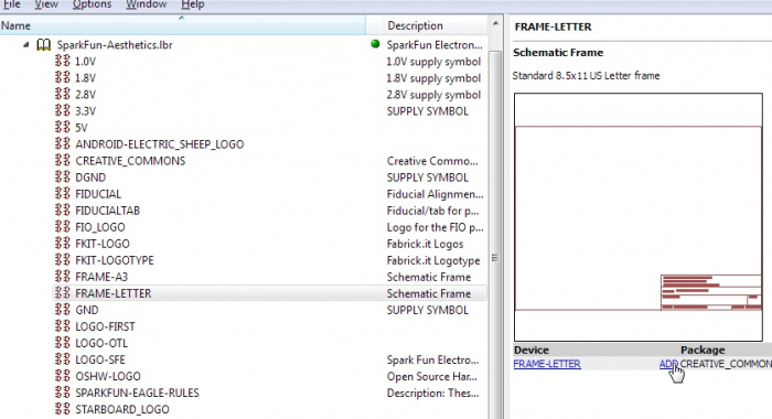
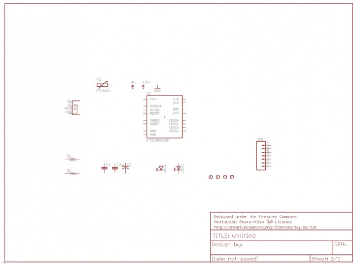
Let’s start by adding a frame to our schematic. From the Eagle main window, navigate to the Libraries folder. Click on the small arrow beside the word 'Libraries' to expand it. Then expand the SparkFun-Aesthetics library (since the frame is just for aesthetics). Navigate to the FRAME-LETTER component and click Add.
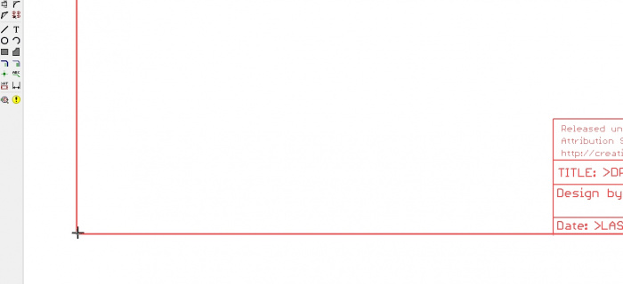
Drop the corner of the frame on the corner of the schematic layout window. Hit escape twice to return to the main schematic window.
Use the scroll wheel to zoom in/out. Press and hold the scroll wheel to drag the schematic window around.
Now let’s add the various bits we’ll need for this example:
- FT230X component from the DigitalICs library. The best way to get to find the component is to click on any component then press ‘f’ to take you to the components that start with ‘f’. Add this to your schematic. Click once to drop the item. Hit escape twice to return to Eagle main window.
- M07 from the Connectors library. You will want the 'M07' device. This is the most common, 7 pin 0.1” header footprint.
- USB from the Connectors library. You will want the ‘USBSMD’ device (it has the ‘USB-miniB’ package type).
- 5V, 3.3V, and GND from the Aesthetics library.
- Two LEDs from the LED library. You will want LED0603. This is the small 0603 sized surface mount LED.
- Two CAPs from Passives library. Get the CAP0603-CAP package.
- CAP_POL from Passives library. Get the CAP_POL1206-KIT package.
- Two Resistors from the Passives library. You will want RESISTOR0603-RES.
- PTC from the PowerIC library. Get the PTCSMD package.
- Four Stand-offs from Electromechanical. Get the STAND-OFF package.
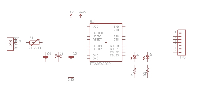
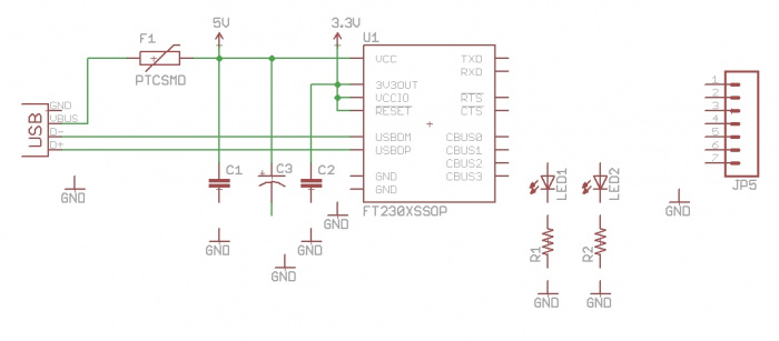
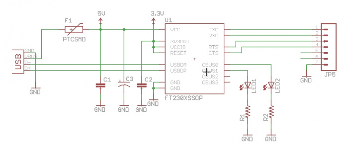
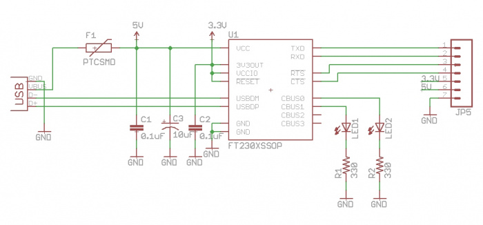
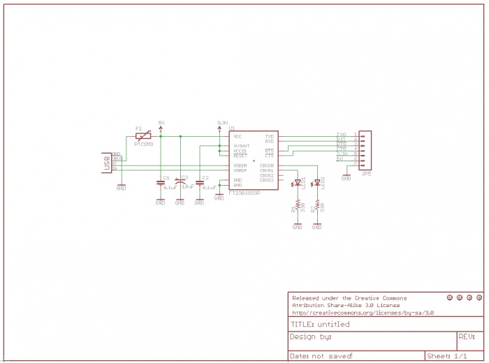
We’ve got all the parts here. Now hit F7 to go into ‘move’ mode. Click on an item and move it around. We’re aiming for the example found in the datasheet. Arrange your components kind of like this:
While you got a component selected and moving, rotate it by right-clicking. Left clicking will set the component down.
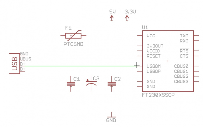
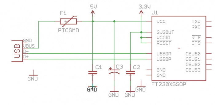
Now press F9 to begin wiring the components together. Click on the end of the D- pin on the USB connector and run it over to the USBDM pin on the FT230X. Click again on the pin and the wire should stop routing indicating that it has been successfully connected.
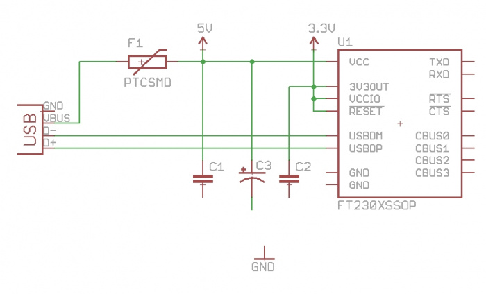
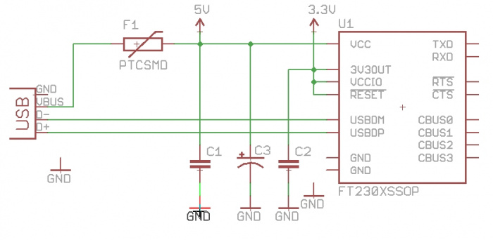
Continue to wire as shown.
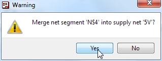
You may get a window that says ‘Merge net segment ‘N$4’ into supply net ‘5V’? or some such warning. The answer is yes you do.
We will need more GND connections. Press F8 to go into copy mode. Click on the GND symbol and create 8 or so copies.
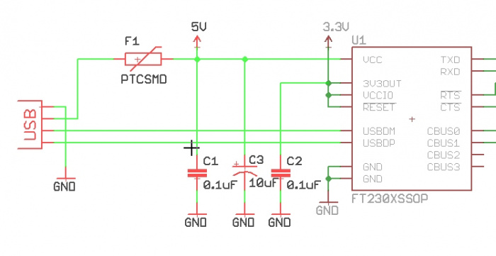
A trick I use a lot is this: Hit F7 to move the GND symbol. Move it directly onto the end of the capacitor and click to drop it.
Now click the same ground symbol and move it down. Eagle will automatically have a wire attached. This saves you from having to do a few wire connections by hand.
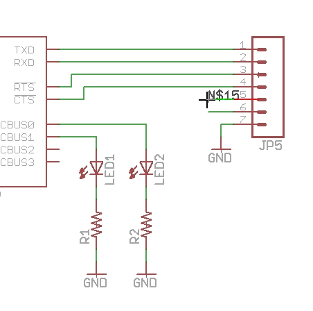
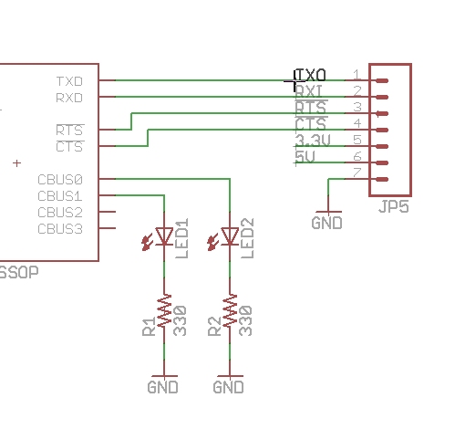
Wire up more stuff. Note the two stubs of wire on pins 5 and 6 on the 7 pin connector. Those are unnamed, unconnected nets.
Press Alt+F9 to go into ‘Label’ mode. Then left-click on one stub. Eagle will highlight the wiring - this is its way of asking if that is the wire you want to be messing with. Left click again to confirm - Eagle will then show a label for the stub. Click again to anchor the label to the stub. Repeat for the 2nd stub.
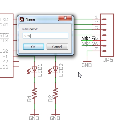
Now press F4 to go into ‘Name’ mode. Click on the first stub. Are you sure you want to connect them? Yes you are. Repeat but name the second net 5V.
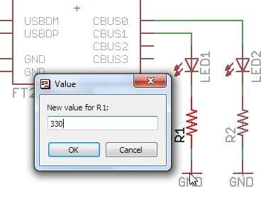
Press F5 to go into ‘Value’ mode. Then click on R1 and set the value to 330. Set the values for the following:
- R2 = 330
- C1 = 0.1uF
- C2 = 0.1uF
- C3 = 10uF
Hey! It’s about time you saved your work! Hit Ctrl+s or the disk icon. Save your work as ‘FT230X-Breakout-v10’. This is the first version so it’s v1.0. If there are changes to be made, save the file as -v11, -v12, etc.
Have a look. The values are sort of running over the wires. Let’s press Alt+F7 to go into ‘Group’ mode.
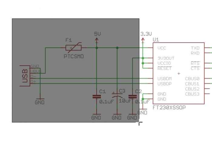
Move the cursor to the upper left corner. Click and hold the button down, then drag to the lower right corner. Note that we are selecting just past C2.
Release the mouse button. You should see a bunch of wires and components selected. Now we've got a group, but we haven't told Eagle what we are doing with this group. Press F7 to go into 'Move' mode. Now let’s move the group! Holding Ctl, click the right mouse button. The group will now be moving with the mouse cursor.
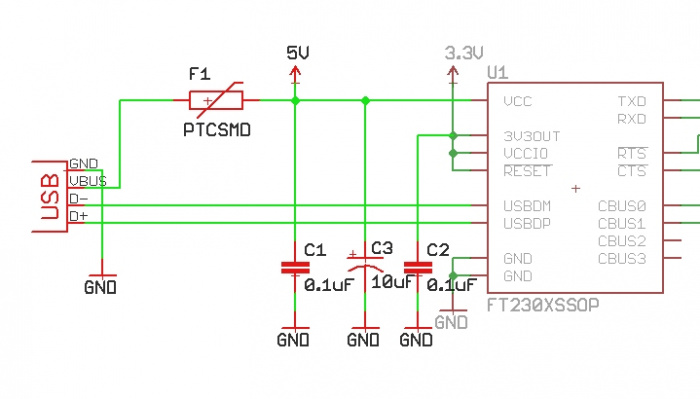
Move it two clicks to the left so that the 0.1uF text doesn't overrun the GND symbol.
Let’s create labels and name the nets near the connector. This will help us in the PCB layout phase. Press Alt+F9 to go into label mode. Click on a wire, Eagle will highlight it. Click again to confirm you want to mess with the highlighted wire. And click a third time to throw a label in that location. Once you have four random labels (such as N$9, N$13, etc), then hit F4 and rename the wires as shown in the picture:
- TXO
- RXI
- !RTS
- !CTS
Note the leading '!' will put a line above the net name (neat!).
Looking pretty good! Let's start laying down traces.
Laying Out the PCB
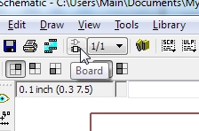
Now let’s click on the ‘Board’ button and start PCB layout!
Yes please create from schematic.
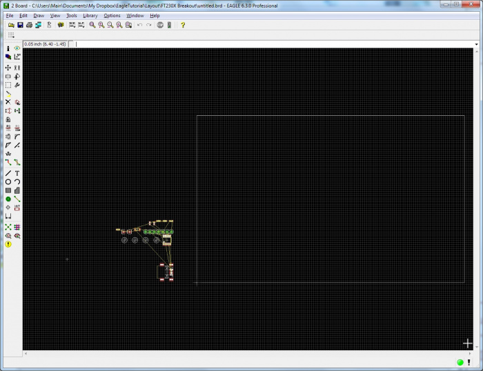
Whoa! Neat! Use the mouse wheel to zoom in and out. Click the mouse wheel and move the mouse to navigate around an area.
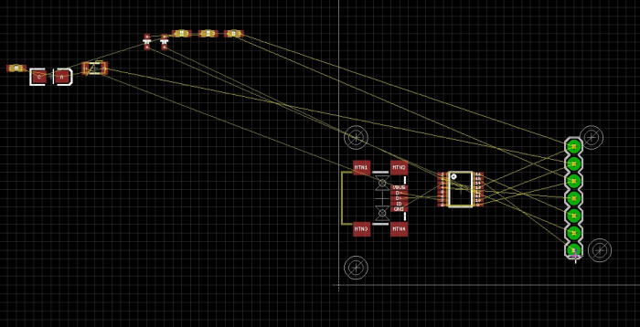
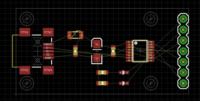
Now press F7 to go into ‘move’ mode. Begin to move the parts to the lower corner of the PCB.
As you’re moving stuff around, right click to rotate a part.
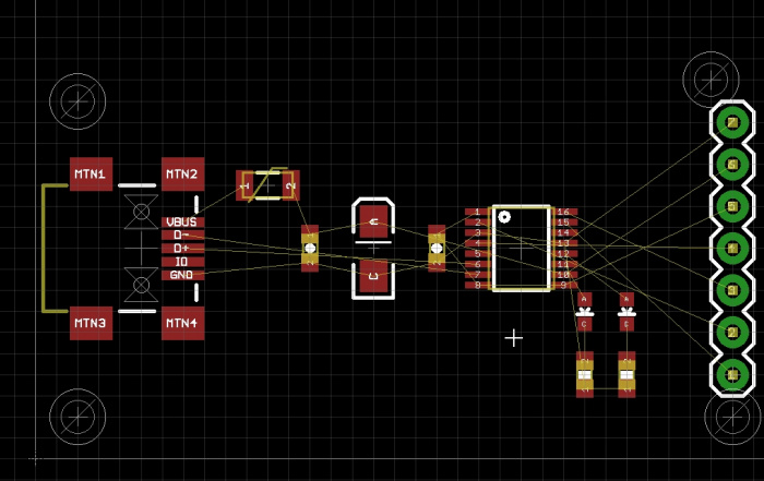
You’ll see the rats nest of airwires update as you go. Be looking to rotate or position a component to try to minimize the overlap of wires. You won’t get it all straightened out but this is the time to be thinking about it. Decent placement at this stage will make routing much easier later on. Regularly press F8 to update the rats nest.
We are getting there.
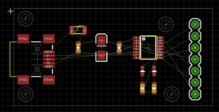
We now need to reduce the board shape to fit our rough arrangement of parts. You should see a thin white wire that makes a big square. This wire is on the dimension layer and represents your outer board shape. Press F7 then click on the white wire and move the sides of the board inward, making a tight box around your components.
Note: The USB connector can hang slightly over the edge.
Also, see the board outline near the cursor is not ‘on grid’? Press F7 to go into ‘move’ mode. Then hold Ctrl while clicking on the corner of the dimension line.
The wire or component (whatever you’re near) will jump onto the grid. This is a valuable trick to get stuff back on grid. Repeat with the upper right corner and lower left corner.
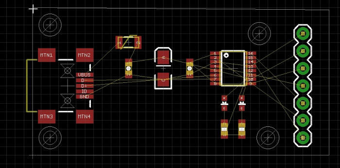
Ok - we’ve got everything packed in together pretty well. Take note of a couple things:
- Draw a horizontal line across the middle of the board. You'll notice I've located a lot of the components along the midline. This helps with aesthetics more than anything but also helps with some routing.
- Do not attempt to pack everything in right next to each other. You will eventually be soldering these parts to the board and will need some room to get the iron and solder wick in there.
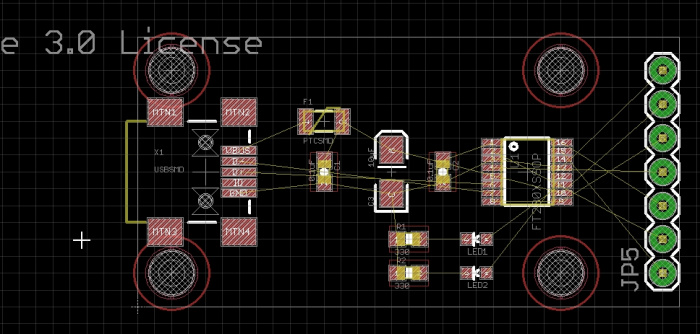
Let’s take a moment to turn on ALL the layers to see if there are any problems. Click on display, then the ‘All’ button, then Ok.
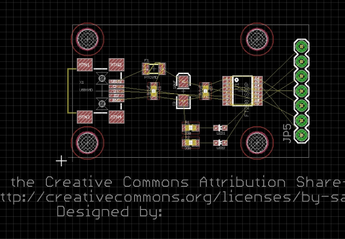
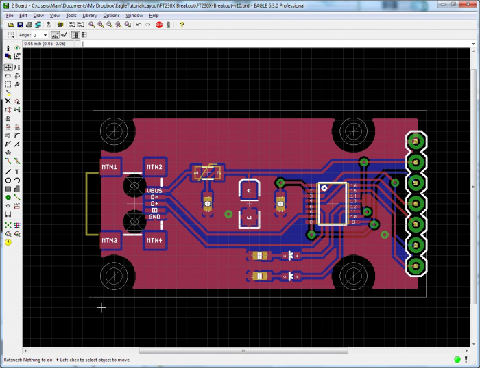
We’ve got a couple problems. There’s some text we didn’t even know about (the creative commons license! Yay!). And you also see red rings around the stand-offs. These rings are on the ‘top keepout’ layer. They are there to show the radius of the head of a standard screw. If we tried to put a screw into the breakout board it would hit the USB connector! Better spread things out.
Use the scroll wheel to zoom out. Hit F7 to grab and move the license below your board.
Remember to use the Alt+F7 group command to group stuff together, then press F7 to go into 'move' mode, then Ctrl+right click to move the group. I used this trick to grab two standoff holes and the frame at the same time and made the board wider. Then grab more bits and bumped them up a few clicks.
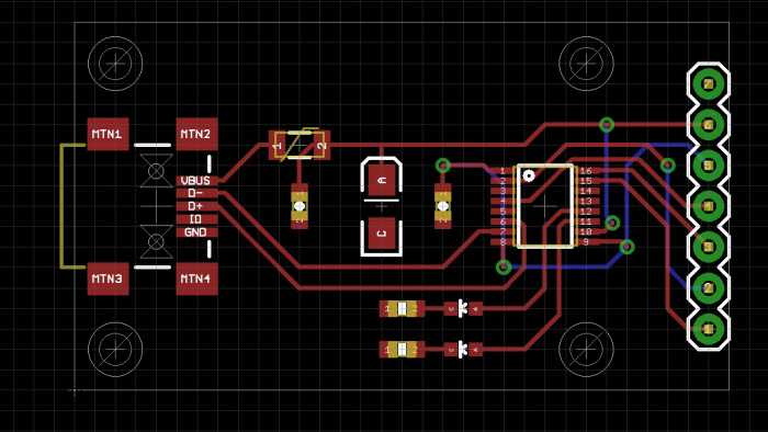
Now press F11 to return all the layers to their original / default viewing state. This allows us to concentrate on layout. Let’s start routing! We’re going to route this board by hand to show more advanced routing techniques. You are welcome to use the auto-router if you please.
At SparkFun we route everything by hand. Yes, everything. This is a change from my views a few years ago. We used to auto-route everything. The boards worked, but they looked awful. We like to think we should be pushing for a board that not only works but also looks good. Did I mention routing a board is like solving a puzzle? And I love puzzles!
Here is a quick breakdown of the key commands we’ll be using:
- Press F9 to lay a trace
- Alt F9 to rip up one
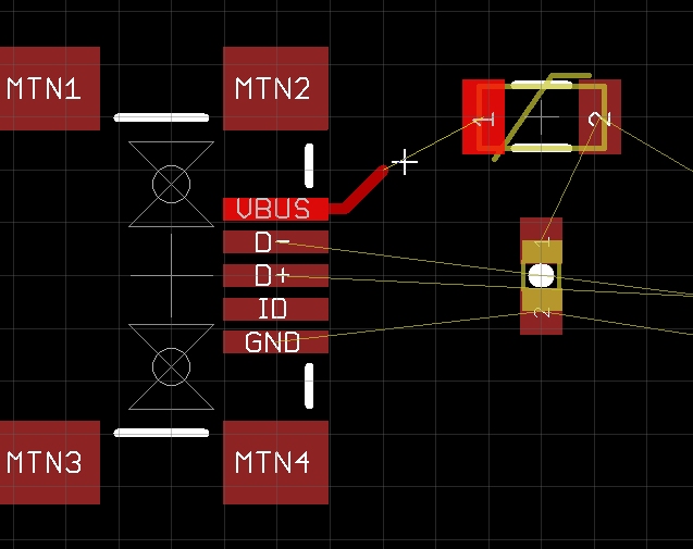
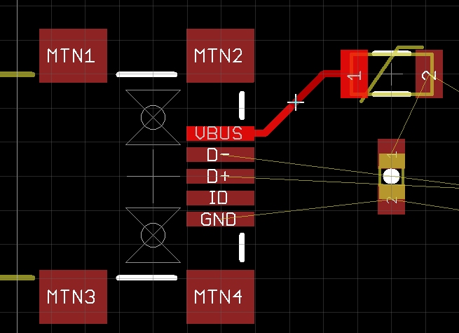
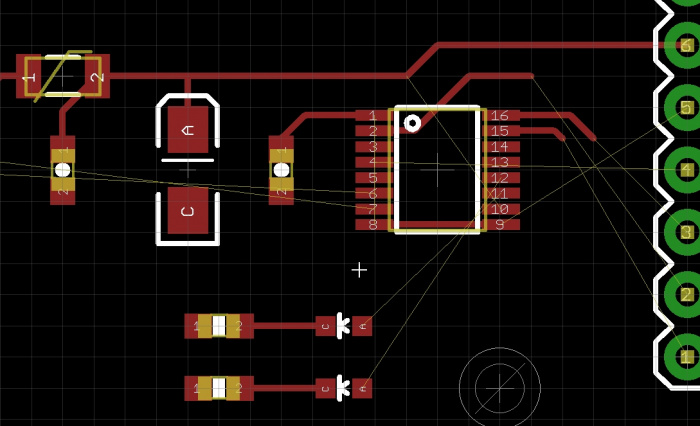
Click on the middle of pad VBUS. Drag out the wire to a grid intersection (it’ll snap to it). Click again to anchor the trace, then click again to stop routing that trace.
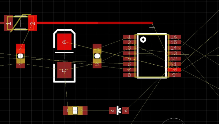
Now start routing from the PTC. Click on the ‘1’ pad. Drag trace out to intersection and down to other trace. You may hear a pleasant ‘ding’ letting you know the trace is completed.
Continue the route after the PTC. Note that it goes down to the right side of the FT230X. I’m worried about boxing out other traces so I’ll just leave a stub of the trace here by double clicking.
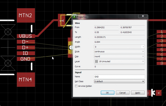
The GND airwires are distracting me. Click on the ‘i’ and then a GND wire. See the box at the bottom that says ‘Airwires Hidden’? Check that box and click ok. This will make all the ground airwires disappear. We’ll get the GND wires with a polygon pour later on.
Start attacking the easiest routes. Leave stubs where you see cross-over problems. See how far you can get without using a via. We'll talk about those next!
Creating Vias
Now let’s talk vias. Vias are a hole in the PCB that have metal running down the inside of the hole so that the traces on the front of the board are electrically connected 'via' the hole to the back of the board.
Press F9 to go into routing mode and look for the Drill box in upper right corner. The default via size in Eagle is 0.02362205” (or more sanely 0.6mm). I change this to 0.02” (or 0.5mm if you please) and press enter to make Eagle save that size.
There is nothing magical about 0.02". This is a size that we've found most PCB fab houses can drill without too many tolerance issues. It’s also small enough to ‘tent’ over with soldermask making the board look a little better.
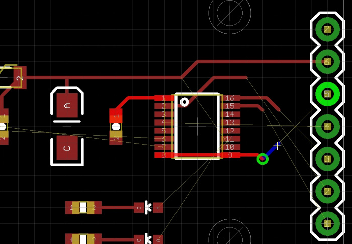
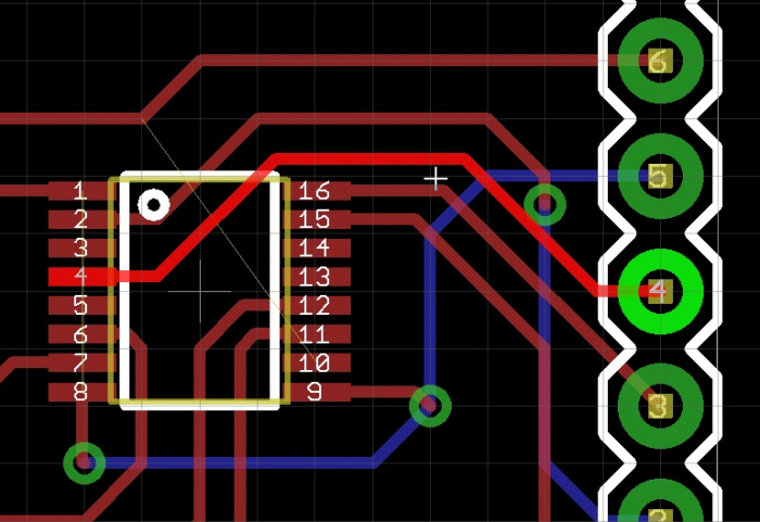
Press F9 to route from a pad. While you’re routing hold the shift key while you left click. This will drop a via and you’ll continue to route on the top layer. Now click the middle mouse wheel. This will drop you to the bottom layer and you can keep routing.
Continue to route some of the other nets.
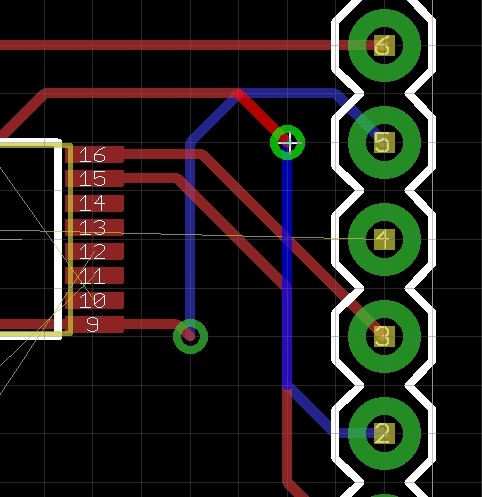
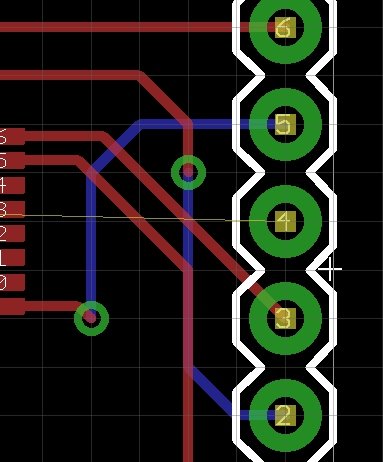
The above routing will work, but if we bump the highlighted via downward, we can straight out the blue trace a bit. Like this:
Nitpicking? Absolutely. But bumping various routes around can make the overall routing a lot cleaner over time.
Note that I keep nearly everything onto the 0.05” grid. This keeps routing and spacing a lot easier. The size (0.05”) is reasonably trivial. The important piece is that all the components and general routing are kept on the same grid.
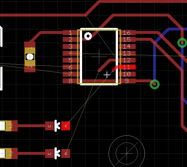
We’ve got two problems here. Two wires could be routed without vias if we ripped up the 8 to 9 route. The two wires also cross over themselves. Re-arranging the LEDs will fix this.
Fixed. However you may note the trace connecting Pin 11 on the FT230 is off grid. While routing, hold the Alt key to jump 'off grid'. Going off grid is perfectly fine but as a rule of thumb, I try to keep on the grid as much as possible.
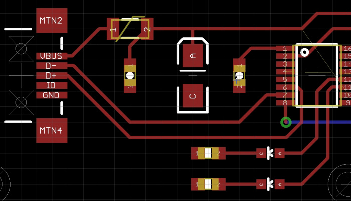
Removing the 8 to 9 route also opened it up so that we could route the D+ and D- traces directly to the IC.
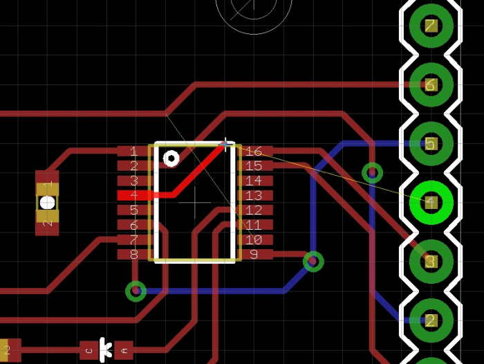
Ah! Neat. If we move some stuff around, we can get !CTS routed without needing a via.
There’s obviously a DRC error here but we can fix it when need be. Let’s just leave it in case other things change.
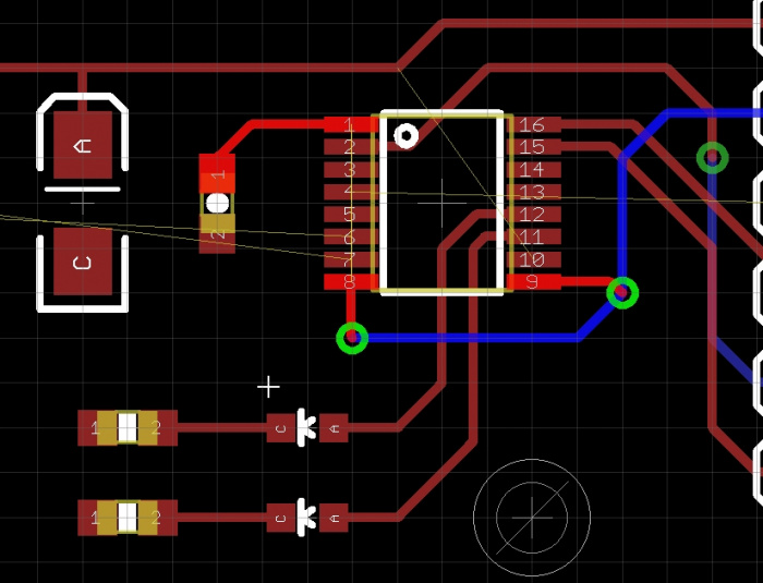
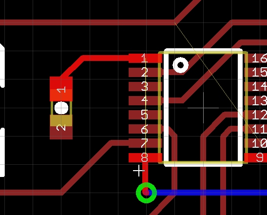
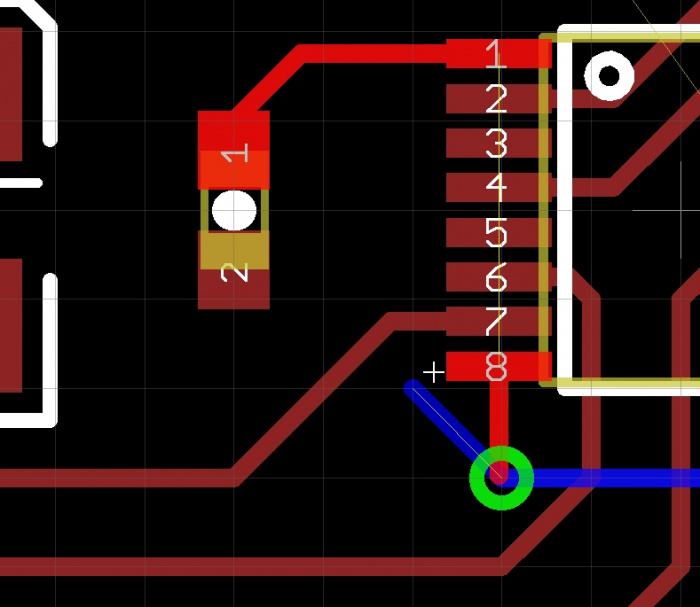
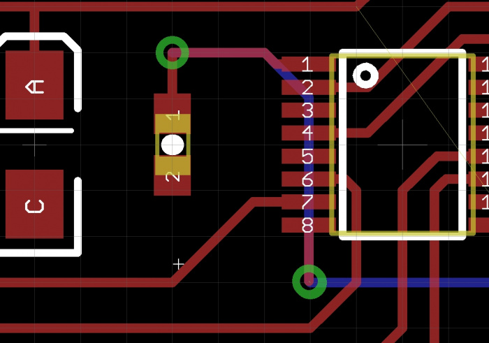
Now I need to get pin 8 connected to pin 1, but Eagle won’t let me start routing from the lower via - it keeps wanting me to route from pin 8. To get around this, I am going to rip up some of the traces near the via so that I can have a starting point. Press Alt+F9 then click on a trace to rip it up.
I ripped up a small trace which gave me an airwire that I started routing from.
Re-routed. Note I still have a very small airwire that I need to route. Not hard, press F9, click on the airwire, click again, and it’ll route.
Next up - we create polygons!
Polygon Pours
Hey! This looks pretty good. Now we need to get GND routed. Let’s do this with a polygon pour.
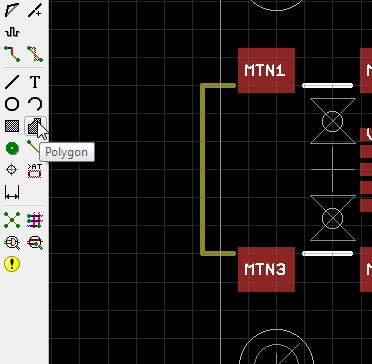
Click Polygon.
Draw a box that follows the dimensional outline, left clicking on each corner.
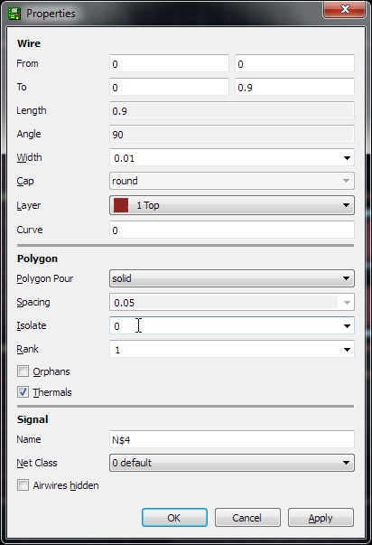
When you close the box it will be come dashed. Now click on ‘i’ and then on the dashed line. This will bring up information about the polygon.
We need to change the isolate from 0 to 0.012”, click ok.
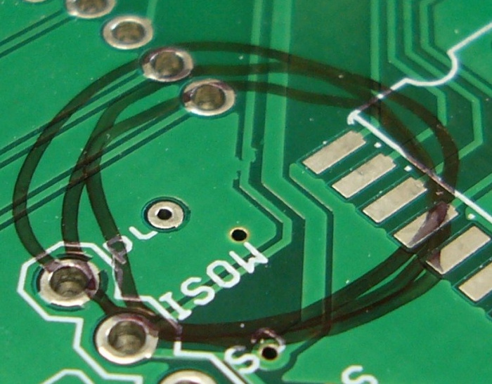
Why change the isolation layer from Eagle's default? We have had multiple PCB fab houses, that produce very high quality PCBs, create polygon pours that accidentally 'run over' onto a trace or pad. This error is rare, but we want to give the PCB fab house an easier job, not a harder one. Increasing the isolation pulls the polygon away from traces and pads just a smidgen, giving the PCB fab house a little more tolerance for error, and increasing the chance that your PCB will come in without errors.
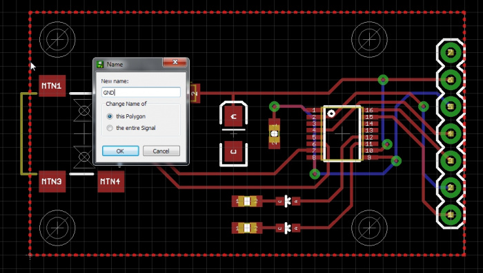
Now to connect the polygon pour to the ground net, press F4 to go into ‘Name’ mode. Then click on the edge of the polygon. Change the net name to GND.
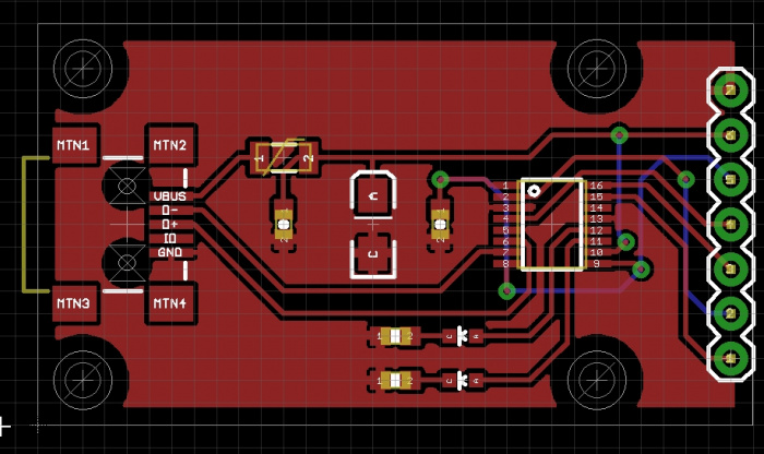
Press F8 to refresh the rats nest. This also causes polygon pours to recalculate. Neat!
Now repeat for the bottom polygon pour. Click polygon, then click the middle scroll wheel and move to the bottom layer. Box the board. Change isolate to 0.012”. Press F4. Name net to GND. Hit F8 to polygon refresh.
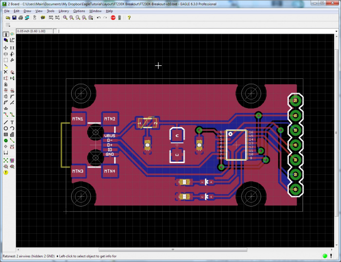
Yay! We have both bottom and top polygons connected to GND. Note the comment in the lower left corner of the window. “Ratsnest: 2 airwires (hidden: 2 GND)”. Uh oh. Looks like we still have a few things to connect. Let’s turn GND airwires back on. Click on the ‘i’, then click on the edge of the polygon. Uncheck ‘Airwires hidden’ and click ok.
Yep. That’s a problem. Let’s create a GND via to connect the various GND islands to the lower layer polygon.
Click on the 'Via' button on the menu and drop the via in a GND island that needs to be connected. This via is not yet connected to GND - it’s unnamed. So press F4, then click again on the via. Name it ‘GND’. Now hit F8 for ratsnest refresh. Neat! One wire gone.
Now that we have a good GND via, we can copy it. Click on the copy button, then click on the GND via we just created. You’ll have a via that is moving with your cursor. Move it towards the GND island on the right end of the board. Drop the via. Hit escape to leave copy mode. Hit F8 to refresh the ratsnest.
Yay! Ratsnest nothing to do! We’ve successfully routed all the airwires. Next we need to label everything on the board.
Adding Labels
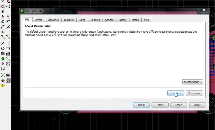
The default DRC rules with Eagle are a little too conservative in some areas, and very bad in others. Let’s load the SparkFun 2 layer standard dru file located here. For this board, we will use Click on the DRC button, then Load.
Double click the SparkFun.dru file then click ‘Select’ in the main DRC window. It should disappear.
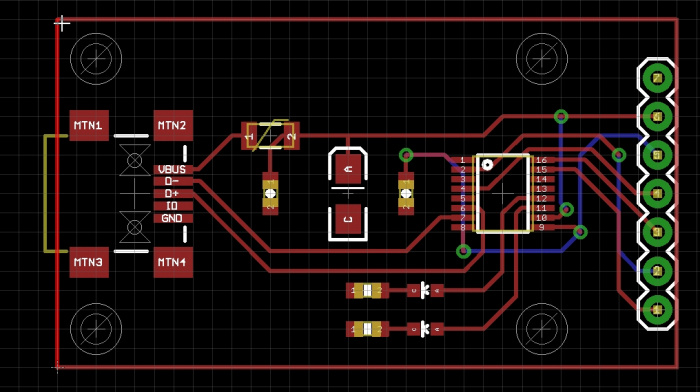
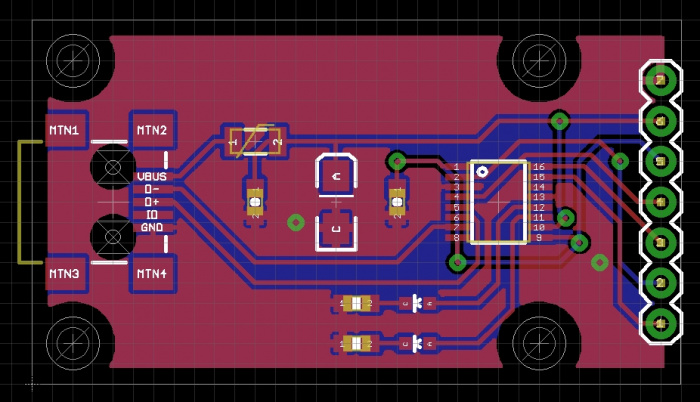
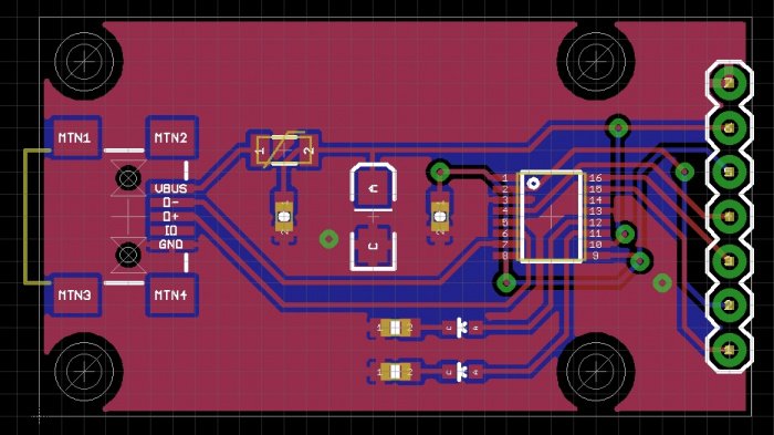
What? It looks the same. But wait! Hit F8 to do a ratsnest refresh. That looks a little better! The SparkFun DRU file reduces the amount of space between the copper layers and the dimension layer (the border of your board) from 40mil to 10mil.
All these vias should work but they are pretty sloppy. The SparkFun design rules file increases the size of the annular rings around your vias. This gives the PCB fab houses a bigger ring to drill through the middle of, thus decreasing the chances the your board will be fabricated with errors.
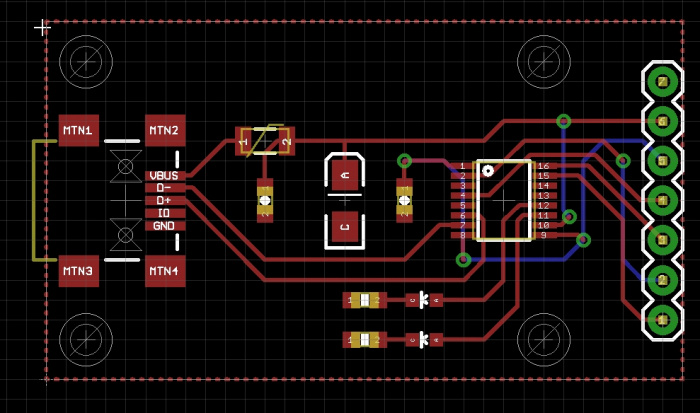
Now let’s increase the width of the board outline from 0” to 0.008”. We do this so that we give the DRC (design rule checker) the chance to tell us if anything is too near the board edge. When the PCB fab house is routing boards apart, they use a very accurate milling machine, but let’s assume they’re not perfect. We use the width of the board outline to give us that level of extra safety.
To change the width of the board edge click on the wrench, then width, then ‘...’. Enter ‘0.008’ then click on the board edge. It will probably highlight the polygon pours. To get around this, right click and the next thing in the stack will highlight - it will probably be the other polygon pour so right click again. Finally the white line that makes up the board outline should be highlighted. Good - now left click to apply the width change. Now do that to the other three sides.
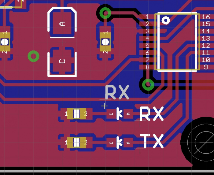
Now it’s time to label everything! Click the ‘Text’ button. A window will pop up, enter ‘TX’.
There will then be text on the bottom layer. No good. Click the middle mouse wheel and select ‘tPlace’. Anything on tPlace will be printed as silk. Hold the alt button and arrange the TX label next to the TX LED.
Pressing escape will bring you back to the text input window. Type 'RX' and add the label next to the other LED.
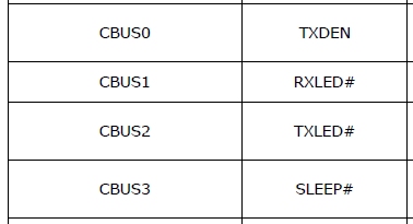
See how the X of TX and RX is bisected? I like centering text. I threw these labels down but I don’t actually know which LED is which. Let’s consult the FT230X datasheet:
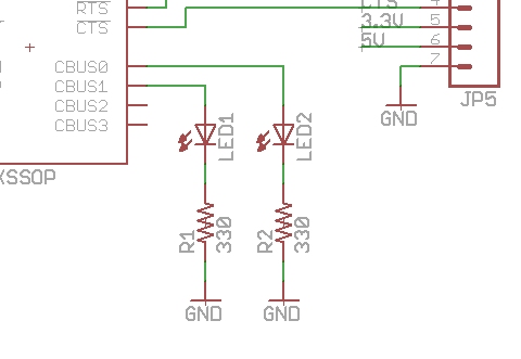
Ok, CBUS1 is RX LED, CBUS2 is TX LED. Let’s go look at our schematic:
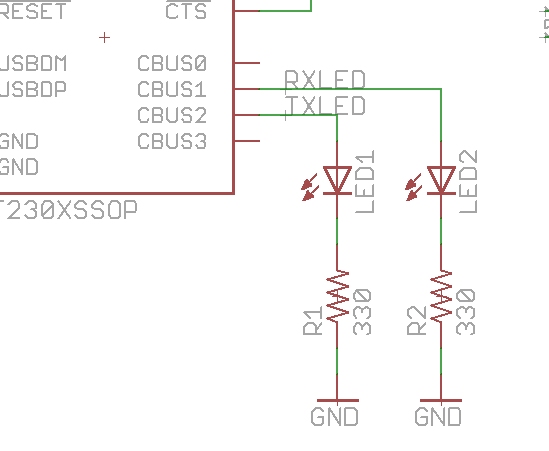
Oh no! I wired it wrong. Let’s delete those two wires (press F3 then click on the wire to remove), group the LED/Resistor/GND (alt+F7 then select, then F7), move them down (ctrl + right click), and add wires back (F9).
Let’s also label the nets so we will know on our layout which is which. Alt+F9 then click on a wire to add a label. Click again to anchor the label to the wire. F4 to rename the wire to RXLED (on CBUS1 pin). Repeat for CBUS2 wire label.
Ok fixed. Let’s go back to our layout.
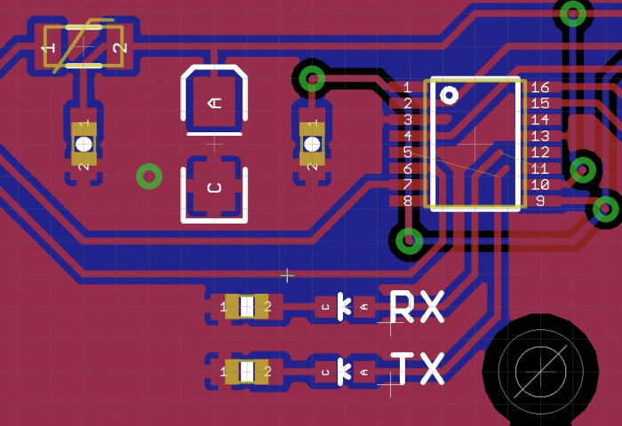
We’ve got some crossed wires. Rip up the traces that were there, swap the LED placement with the alt-F7 group command then re-route.
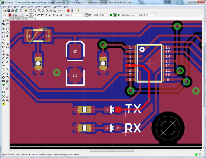
Rerouted. Now press F12 to ‘Show’ trace names and click on a trace. You will see the name of the net in the lower left corner of the Eagle window. ‘TXLED’ is now labeled correctly.
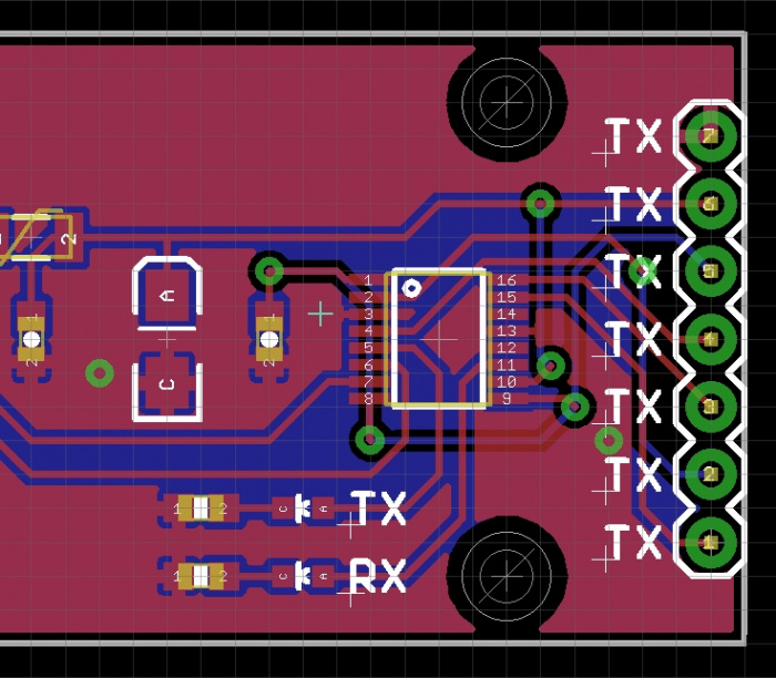
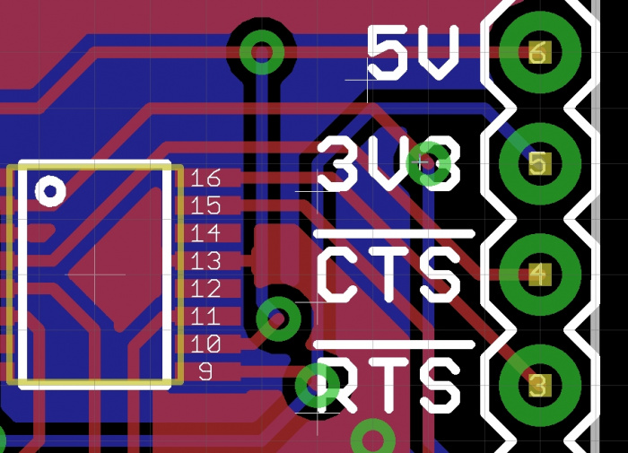
Copy the TX label a bunch more times. Press F12 and click on each trace to figure out what is there (Remember when we named the nets on the schematic? Here’s where it pays off). Then do a ‘Change’ wrench -> Text and change each label to what each pin actually is.
Is the text size a little too large for your taste? You can use the wrench to change 'size' as well. We prefer 0.05" or larger so that the text is easier to read.
Remember: the PCB fab house has limits to what it can do. We've found that anything smaller than 0.04" turns into an unreadable white blob.
Now do some label centering. See those vias in the middle of the labels? The user will probably be able to read the label, but let’s move the two vias in order to make the label unbroken.
Is moving vias out of the way of text unnecessary? I would argue it is necessary. The board only has value if you know how to hook up to it. And I'm not talking about in the next week or two, I'm talking about when you're soldering on a ladder using a head lamp and you're not sure which spot to solder the sensor to... Clear labels make or break a project.
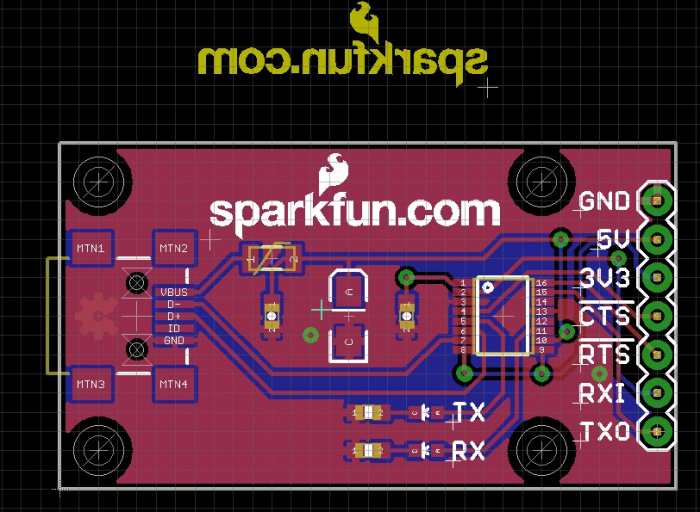
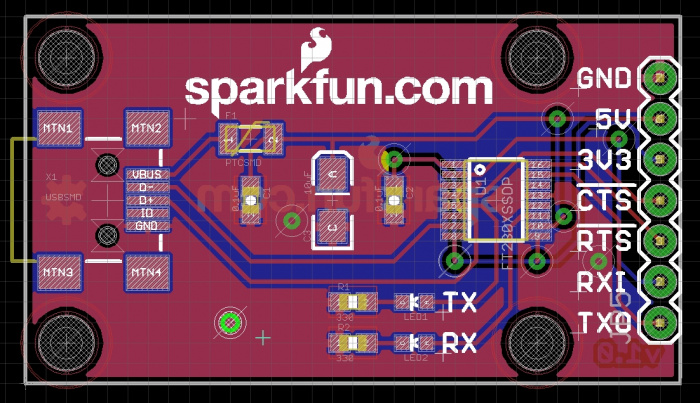
I am getting pretty happy with this layout. Let’s add some finishing touches. Because we’re SparkFun, we throw our logo on everything. We’re also a big proponent of the Open Source Hardware initiative. From the Aesthetics library, let’s add two of the LOGO-SFE and one OSHW-LOGO.
I sometimes have to add some lines on the tDocu layer to show me center point on the board. I draw these in by hand then remove them once I’ve used them to center a logo or text label.
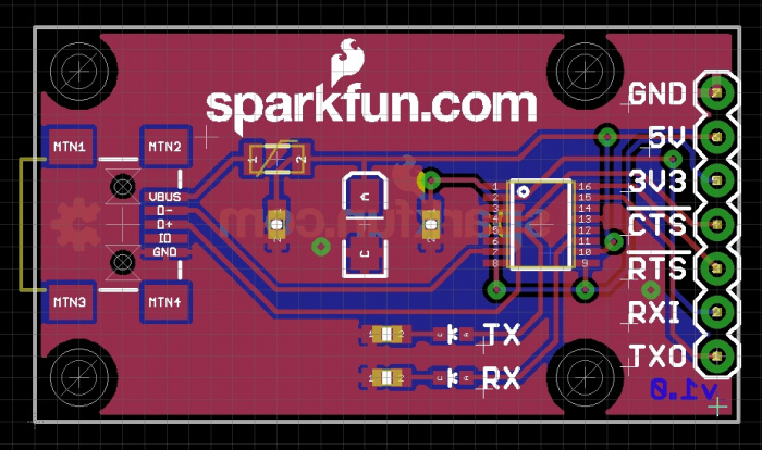
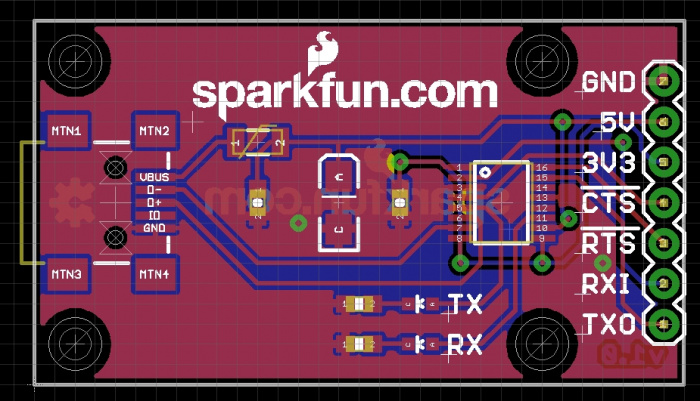
This is version v1.0 of the board so add that text, in copper, to the bottom of the board. Hit F8 to ratsnest refresh and see the text in the bottom copper.
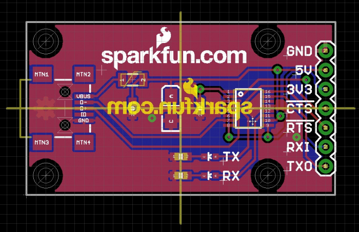
Now for some sanity checking. I’ve turned on all the layers to be sure that the vias will be tented (covered up by the solder mask). You can see in the screenshot that there are white hash marks on most SMD pads and on the large 0.1” connector on the end of the board. The smaller vias however do not have these hash marks. The DRC rules are set up (see the Mask tab under DRC) to mask over any hole 0.020” or smaller. I’ve added a larger via to show this point. This larger via would be exposed.
There are a few circumstances where we expose a via or two - usually for test points. We use a spring loaded pogo pin to make contact with that point on the board so that we can test the board more easily. But in general, all the vias on SparkFun boards are masked over for aesthetic reasons.
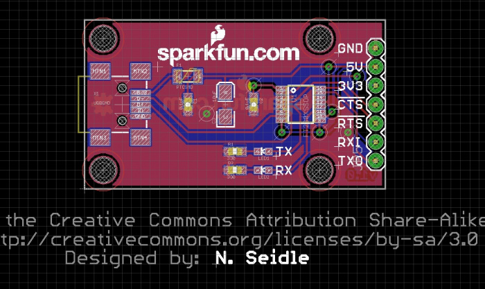
Lastly, we add the designer’s name to the PCB and schematic. This is to maintain attribution whenever the design gets reused or modified. It’s also nice to know who to talk to if there are support questions.
Design Rule Check
Time to run DRC on the board to make sure we've not made any electrical or mechnical mistakes. Let’s turn off the extra layers by pressing F11 and click on the DRC button, then ‘Check’.
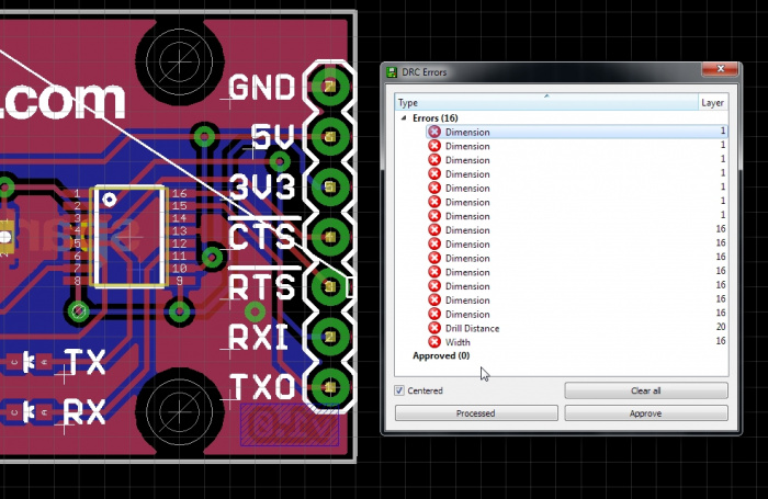
Hmm... We’ve got some errors. This dimension error is because the annular ring of the connector is too close to the edge of the board. Remember when we increased the width of the board outline? This is being raised because of that. The risk here is that when the board is milled out it may nick the annular ring of this connector. SparkFun has a general policy that this is ok and this type of error, on a 0.01” connector can be dismissed. In the rare event that the ring is nicked, the connection and therefore the signal will survive. Click on ‘Approved’ through all the dimension errors.
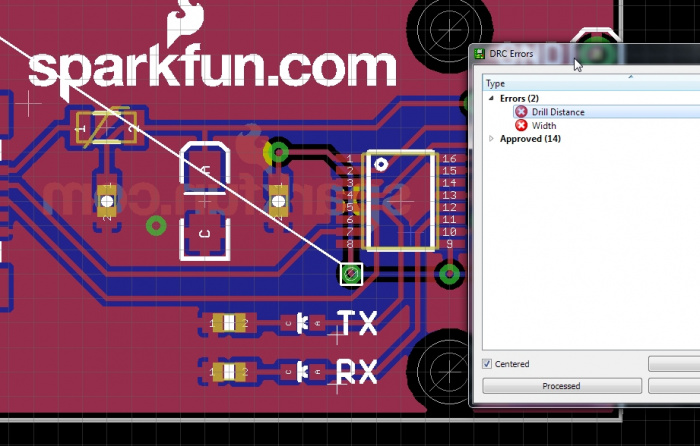
This is a valid error! Looks like I accidentally created two vias, right on top of one another when I was routing that really small airwire. To fix this, let’s alt+F9 rip up and click on that via to see if we can remove one.
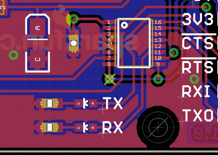
We’ve removed the via but Eagle is trying to tell us (with a big X) that something is still wrong. Hitting F8 ratsnest refresh doesn’t help, so I’m going to rip up those traces and re-route.
I ripped up those traces, then rerouted. I then re-ran DRC and Eagle is now happy. Error cleared.
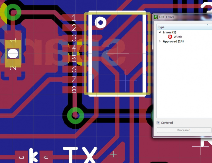
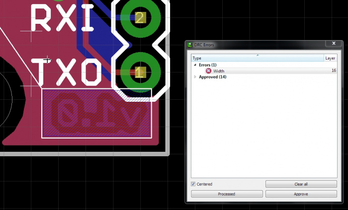
This is Eagle trying to tell us the trace width of this text is too thin. Normally fab houses don’t want traces thinner than 8mil (0.008”). This text violates that. Obviously, we and the fab house don’t care if these traces are broken because 'v1.0' is for informational purposes, not for signals. But the real way to correct this is to increase the text ratio so that the traces get bigger than 8mil. Hit the ‘i’ button, click on the text and increase the ‘ratio’ to 20%. Re-run the DRC and the error should clear.
Ok. We’re close to the finish line. Hit F8 and make sure there are no remaining airwires. Run DRC one last time to make sure there are no DRC errors.
I often turn off everything but the top layer and look at the trace routing. Are there any traces that do anything really silly? Then I do the same for the bottom layer.
Gerber Generation
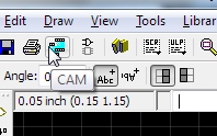
This layout is done! Now let’s generate some gerbers and get this board made! Hit F11 to turn on all the standard layers then click on CAM. If you don’t have the SparkFun CAM file, grab it here and put it in your Eagle\cam directory or, what I recommend, is to put this CAM file on a Dropbox folder that way you use the same CAM file between different version of Eagle and different computers.
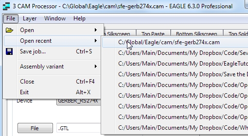
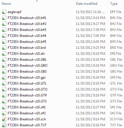
From within the CAM window, click on File->Open and located the sfe-gerb274X file. Once you’ve got the sfe-gerb274x.cam open, click ‘Process Job’. A few windows will pop up then close. Now go look in the folder that contains FT230X-Breakout:
The *.brd and *.sch files are the main Eagle files. If you want to post or share your design with a friend online, these are the two files you need to zip and send them.
All the files ending in *.b#1, .b#2, .s#1, .s#5, etc are backups. Every time you save the schematic or board Eagle will create a new b#_ file and save the previous brd file to it. This is handy if you need to revert back to a version you were working on.
The *.gpi (general photoplotter information) and *.dri (drill information) are generally not needed by the PCB fabrication house.
The main gerber files you need to grab:
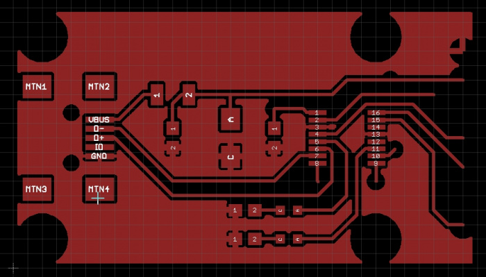
- *.GBL - Bottom copper layer
- *.GBO - Bottom overlay (silkscreen)
- *.GBS - Bottom soldermask
- *.GTL - Top copper layer
- *.GTO - Top overlay (silkscreen)
- *.GTS - Top soldermask
- *.TXT - Drill file (coordinate information)
Note there is no dimension file in this list. The dimension layer gets exported to the top copper layer using our CAM file. Your fab house can probably work with this but may want something different.
You will probably see a *.GTP file. This is the top paste layer. At SparkFun, we use this layer to have a paste stencil cut. Stencil solder paste and doing SMD reflow is super helpful if you are running more than 3 or 4 boards. You can absolutely stencil, build, and reflow PCBs without big, expensive equipment! And you can even cut stencils at home.
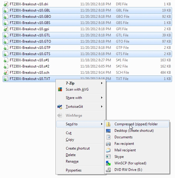
Select the gerber files and drill file, 7 in all. Do this by clicking on the first file, then hold Ctrl, then click on each additional file. Right click and under Windows 7 you can Send To a zip file. Zip together however you are most accustom.
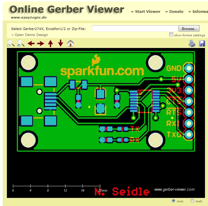
I just recently found www.gerber-viewer.com. They have a pretty good interface for inspecting your gerber files. I highly recommend you use a gerber viewer separate from Eagle before you send them off.
With your gerber files in hand, email your favorite PCB fab house. Most fab houses are setup to do:
- Silkscreen one side
- Green soldermask
- White silkscreen
- 1.6mm thick FR4 PCB
Almost all PCBs have these specs but doing fancier PCBs is getting cheaper and cheaper. All our products are made with red soldermask and have silkscreen on both sides. Our LilyPad line is 0.8mm thick with purple soldermask. If you’re just doing protos, stick with the standard setup. If you’re doing a production run, get creative!
Now go play some Portal 2 while you wait for your PCBs to come back. It can take anywhere from a few days to a few weeks to get PCBs manufactured.
Resources and Going Further
We hope you've enjoyed reading this tutorial on how to layout an SMD based PCB! Now that you know how to layout SMD PCBs, here's some further topics you may enjoy reading:
- Connector Basics
- SMD Soldering
- Stenciling and Reflow
- Creating SMD Footprints
- Electronics Assembly
If you'd like to share your PCB creations with the world, check out these tutorials:
