Electronics Assembly
 Nate
Nate 
The Steps
SparkFun has some very unorthodox methods for assembling electronics. We’ve compiled some of the steps and the lessons we’ve learned over the past decade of DIY PCBA (printed circuit board assembly). We’ve grown to a point where some of this doesn’t make sense to do in the basement of your house, but if you’re wondering how we do what we do (build over 80,000 widgets a month), read on.
We are going to start at the front of production. This means the design has already been vetted, prototyped, reviewed, and ‘gone to red boards’ (once a green colored prototype is ready for production we have the PCB made in red). Now we just have to build the thing!
If you’re completely new to electronics, you might want to checkout PCB Basics.
PCB Basics
An electronic assembly at SparkFun typically goes through seven steps:
- Paste Stenciling
- Placement
- Reflow
- Manual Assembly
- Inspection and Testing
- Washing
- Packaging
Here’s a quick video to show you all the steps in one, awesomely silly, video:
Now let’s go through each step...
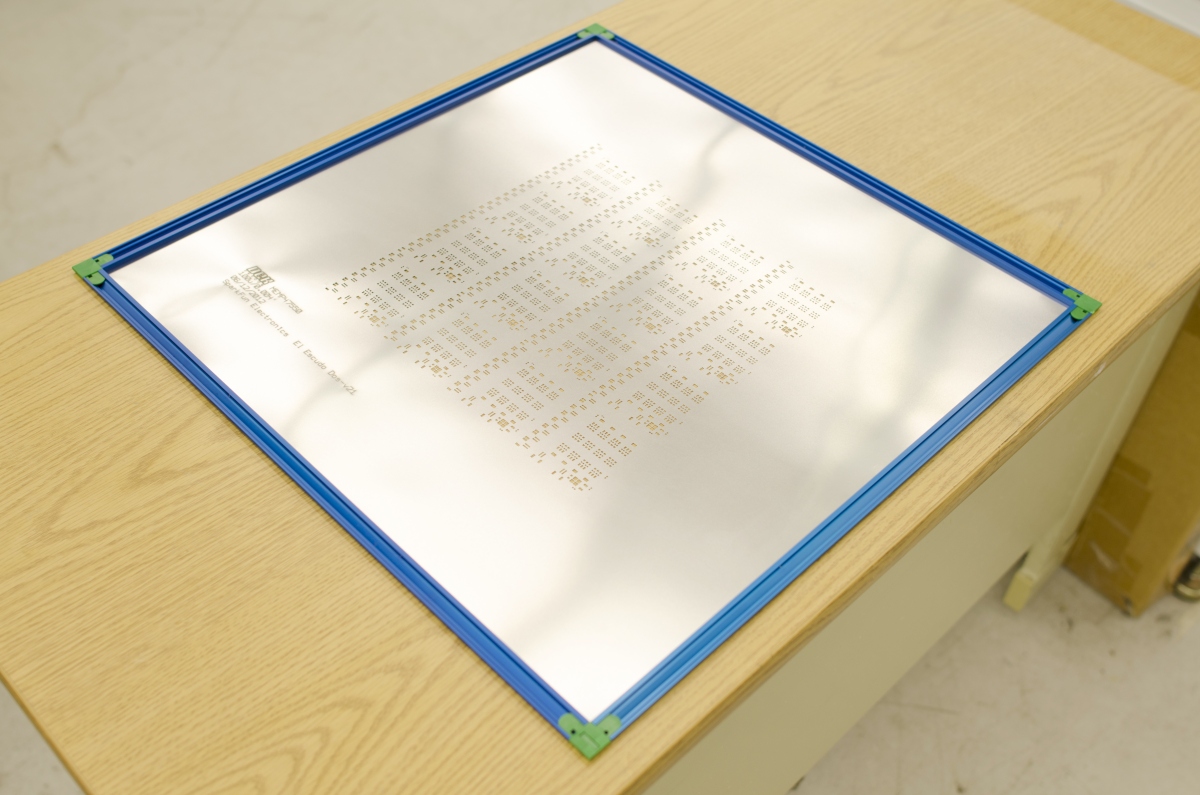
Stenciling
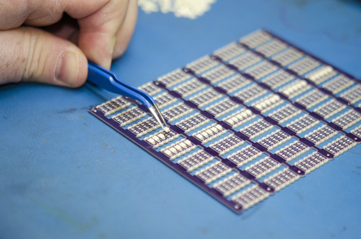
Solder paste stenciling is a lot like silk screen stenciling a t-shirt. You have a mask that you lay over the thing you want to apply ink to. In our case we use a metal stencil to apply paste to very specific parts of a PCB (printed circuit board).
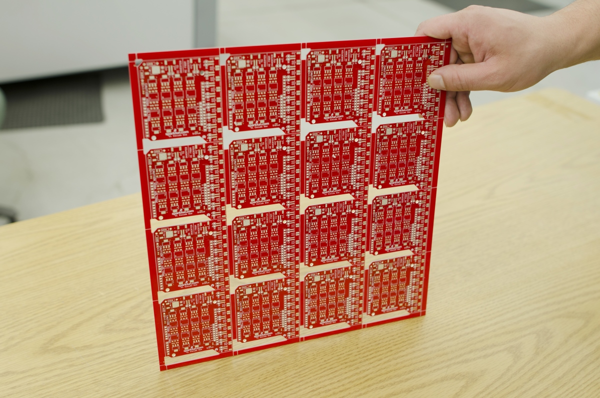
At SparkFun, we start with a PCB panel. Panels are a larger board with the design repeated several times over, to make handling easier. In this case we have 16 copies of the EL Escudo Dos. We make these larger panels so that we can stencil multiple boards at the same time. However, you can just as easily stencil one board at a time.
A small dab of solder paste is placed on each pad where a component will sit. To make this process faster, a stencil is laid over the board, and the paste is smeared over the stencil with a metal squeegee.
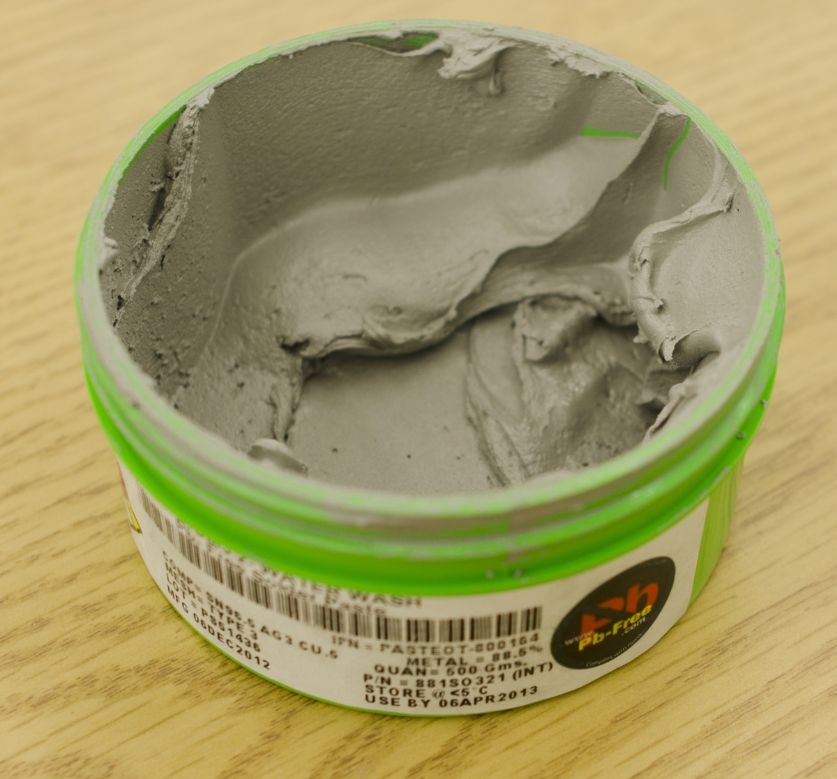
This is what solder paste looks like in the wild. It’s a mixture of metal alloys: 96.5% tin (Sn), 3% silver (Ag), and 0.5% copper (Cu). Most paste has an expiration date and should be stored in a cool place. This has to do with the flux that is added to the metals thus creating the paste consistency. Flux changes the surface tension of the metal when it is in liquid form helping it to flow into the joints.
We use lead-free solder paste but if you’re not planning on selling your widget in Europe then leaded paste is a little more forgiving and easier to use.
We design all our boards in Eagle PCB. The software outputs various layer files that the PCB manufacture uses to create the actual PCB. There are also two layers (top paste and bottom paste) that we send to our stencil fabricator. They use a high power CO2 laser to cut the stencil out of thin stainless steel sheets.
Stenciling can be done by hand. In the video above, Abe does a quick demonstration of how to line up a stencil and apply solder paste. Checkout this awesome presentation for some additional photos and information about stenciling.
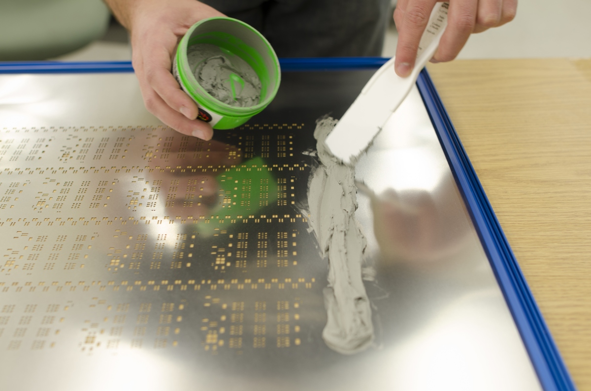
There is no magic when globbing paste onto a stencil. We like to use off the shelf putty knives from the local hardware store.
Here's the stenciling machine at SparkFun. It's a lot of work to setup the machine, but for very large runs (greater than 500 pcs), it makes stenciling a bit easier.
Pick and Place
Once the board has paste applied, the components are placed on top. This can be done by hand or by a machine. Using tweezers is a great way to place components. There is a common fallacy that you need large, expensive machines to make electronics. Not true! A human is quite fast at placing components and the surface tension of liquid metal is such that most components will shift into their correct location during reflow. But humans have a limit to their stamina. After a few hours it becomes harder to place components quickly. The small size of the components also tend to strain eyes.
SparkFun started by placing all the components by hand and we still do! But if we have more than about a hundred units to build we use a pick and place machine to allow us to build lots of boards.
A pick and place (PNP) machine is a robotic assembly device that uses a vacuum to lift a component off of a piece of tape, rotate it to the right orientation, then place it on a circuit board. It takes a few hours to setup a machine to build the assembly, but once everything is running, it is very fast.
In a large factory, a conveyor belt often carries the board directly from an automated paste deposition machine into the pick-and-place machines; at SparkFun, we move our boards manually around the production floor.
Reflow
After pick-and-place, the paste must be reflowed to create a solid solder joint. The boards are put on a conveyor belt that moves slowly through a large oven, exposing the boards to enough heat to melt the solder (about 250°C!). As the board moves through the oven, it encounters different temperature zones, allowing it to warm up and cool down at a controlled rate.
Here we have the control board for the infamous Portable Rotary Phone with components placed on the solder paste. The paste is tacky like butter sticking to a dish. The components stay in place while the board slowly moves through the reflow oven.
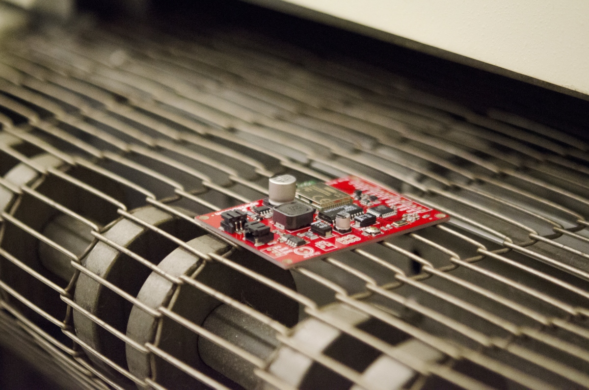
The reflow oven is kind of like a pizza oven. The board is raised in temperature to about 250°C (~480°F) at which point the paste turns to liquid metal. As the board exits the reflow oven, it quickly cools soldering all the components in place.
The video shows a DIY toaster oven showing the various stages of reflow. At the beginning, you can see the little gray blobs of solder paste on the various pads. This paste was probably hand applied rather than stenciled on; you'll see why that sloppiness factor doesn't matter so much later in the video. At about 1:05, the first milestone is passed: the flux within the paste gets runnier and begins to form puddles. The metal solder has not yet melted. At about 3:10, the solder starts to melt, and the surface tension of the molten solder causes the puddles of melted solder to form the smallest possible object: a blob centered on a pad.
You can also see the degree to which the solder can move the parts around as it reflows. Some of the parts end up misplaced and will need to be reworked later. However, this tendency to contract and move parts means that small misalignments and stray solder tend to be largely self-correcting problems. With really tiny parts, however, if one end of the part is pulled harder than the other, the result can be a part standing on end; that's called tombstoning, and it causes a functional defect in the board.
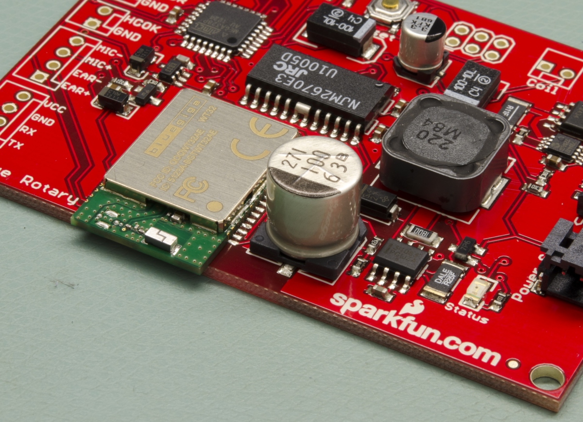
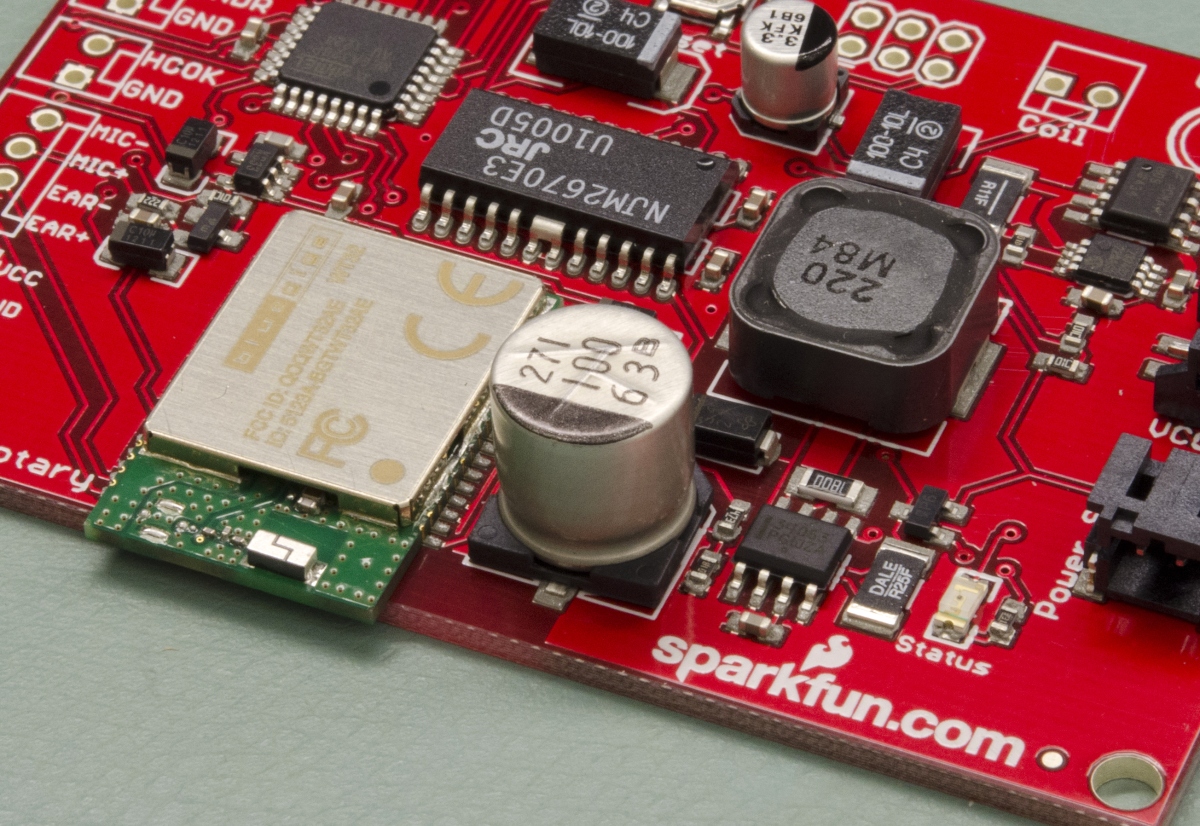
Cool to the touch, this board now has all the SMD components fully soldered to the PCB. The board is now ready for the next step!
How do you do two sided boards?
A few of our assemblies (the Arduino Fio for example) have parts on both sides of the board. In those cases, the side with the fewest and smallest components is stenciled and reflowed first. Once the board is out of the reflow oven it is stenciled on the second side, placed, and reflowed. The surface tension of metal is very high and holds everything in place. In factories with larger, more complex assemblies various bits of the board may be glue in place during the pick and place step to insure the component doesn’t move during reflow.
Manual Soldering
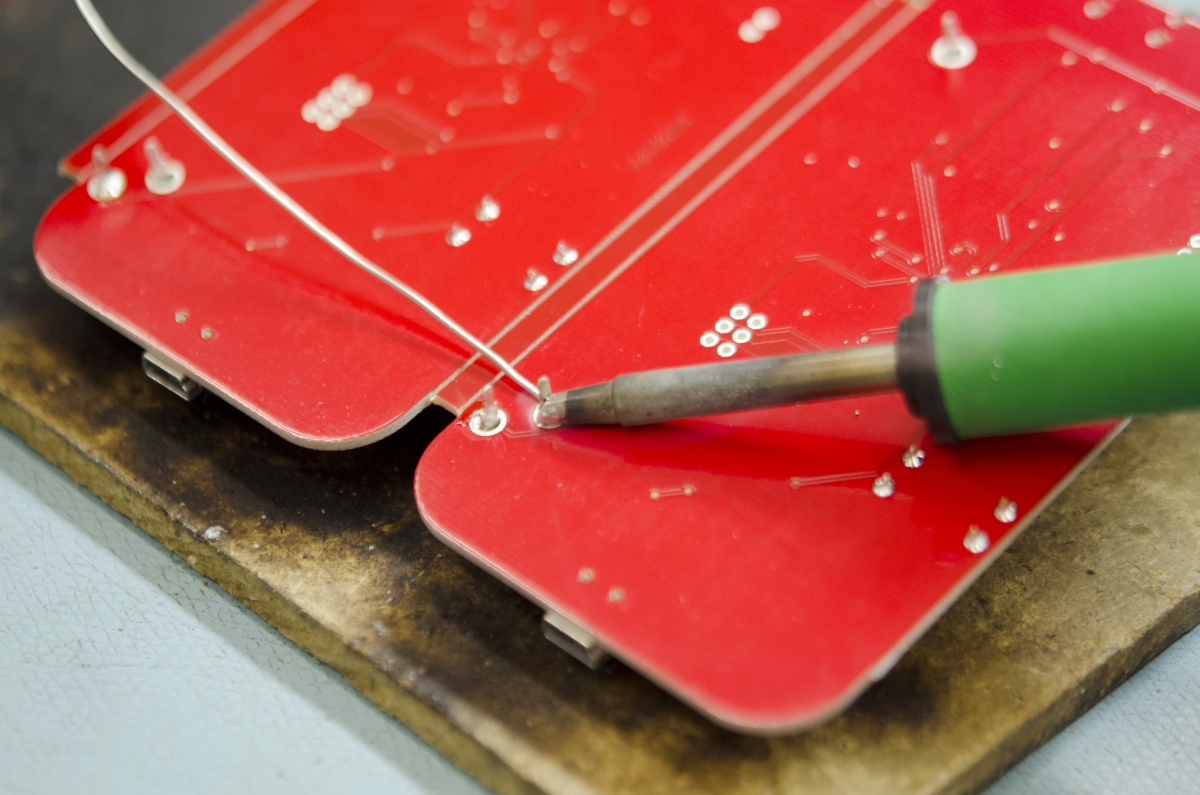
After reflow, a technician takes the board and manually solders any PTH (plated through-hole) components. In a larger production facility, the soldering of through-hole components may be done using a technique known as wave soldering, where the board is passed over a standing wave of molten solder, which adheres to component leads and any exposed metal on the board.
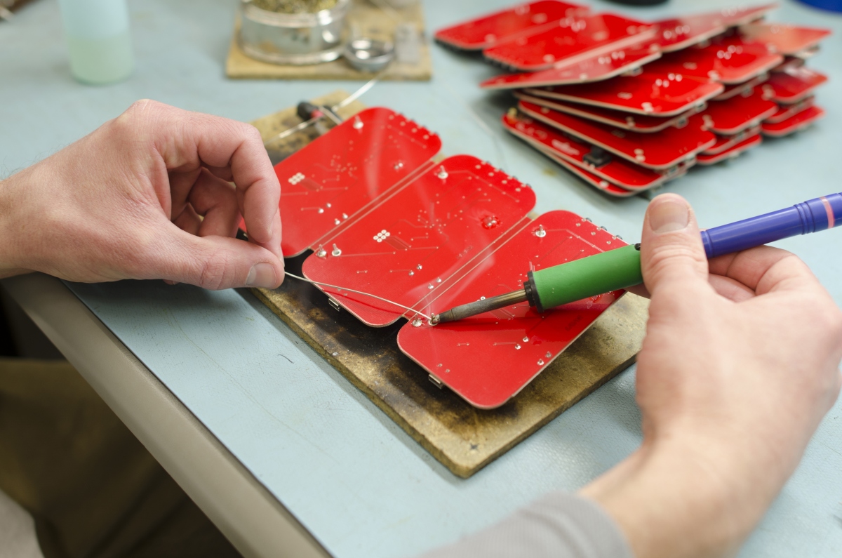
Because of the high mix of different designs and quantities at SparkFun, we’ve found it’s easier to push as much as possible to SMD (surface mount devices) and hand solder any PTH components. We use the Hakko FX-888D soldering iron on the production floor. They work fabulously, but the lower cost Atten 937b is great for entry level soldering.
Inspection and Testing
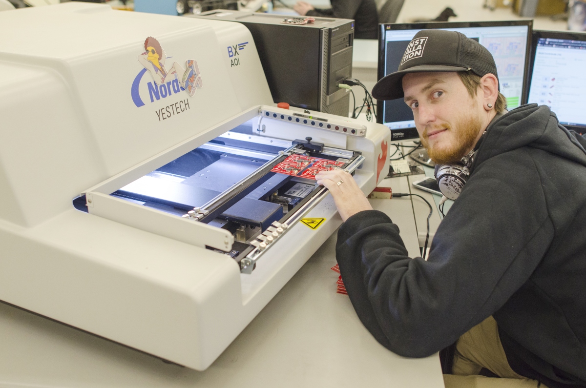
The next step is optical inspection. Optical inspection catches any problems with parts (wrong resistor, missing cap, etc.). The AOI (automated optical inspection) machine is fast. You watched the video, right? That’s very close to real time. The AOI uses a series of high-power cameras at different angles to see different parts of the solder connections (sometimes called fillets). Good and bad solder fillets reflect light differently so the AOI using different color LEDs to illuminate and inspect every connection, with great accuracy, at high speed. It’s pretty sweet.
Do you need optical inspection for your board? Probably not. We didn’t get one until we were doing 30,000+ boards a month when it was becoming harder and harder to catch all the errors.
We run the majority of boards through our automated optical inspection (AOI) machine. Optical inspection checks to make sure all of the correct components are on the board, in the right places, with correct solder fillets and no solder jumpers between adjacent pins.
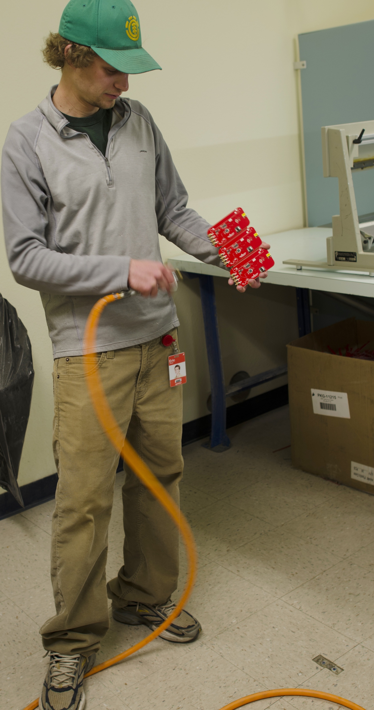
Once the board has been inspected it is tested to make sure it does what it is supposed to do.
Imagine if it takes 15 seconds to test a board. What if you have to test 10 boards? That’s about 3 minutes. What about 1500? That’s over 6 hours of mind numbing testing. We spend a tremendous amount of time making our test procedures and programming as quick as possible.
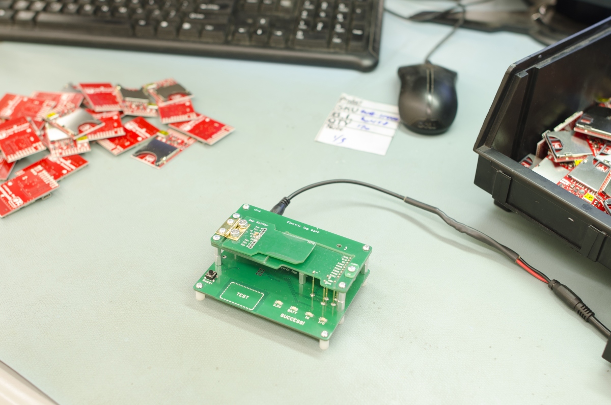
To speed up this process, our technicians use a test fixture, sometimes called a pogo bed to allow for quick testing. Pogo pins use a spring loaded head to create a temporary electrical connection to the various points on the board for power and data. Once the board or panel is loaded onto the pogo bed we run various tests to make sure the board is fully electrically functional. This may include testing the voltage output of regulators, expected voltages on certain pins and sending various commands to the board under test to make sure it responds correctly. On boards that require programming or calibration, additional steps are taken to load code and verify the output.
Larger facilities may use flying probe or bed of nails fixtures to test every connection on a board for continuity before powering the board. These larger fixtures are good for more complex, expensive products but can frequently run into the tens of thousands of dollars to create.
Washing
Various steps of the manufacturing process leave residue on the board. If you've ever put one of our kits together, you know that soldering leaves a small amount of flux on the board. Over a period of months this flux residue becomes sticky, looks horrible, and can become slightly acidic leading to a weakening of solder joints. To prevent this (and to give our customers the best looking boards) we wash every board we produce.
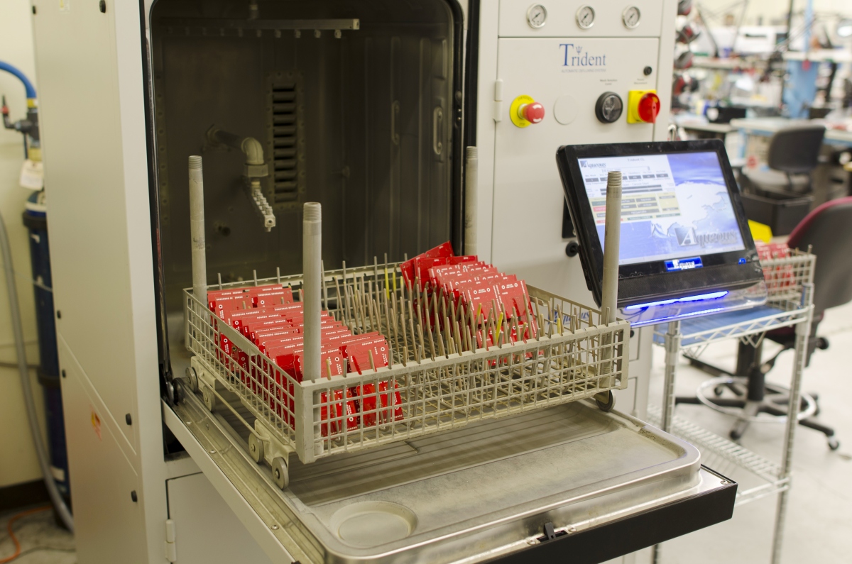
To get the boards clean again we load batches into what we call the 'dishwasher'. This high temperature, high pressure, all stainless steel dishwasher uses deionized water to remove any residue from the manufacturing process.
The parts washer uses a closed loop system. After the completion of a wash, the waste water is collected in a basin below the washer and automatically tested for conductivity. If the electrical conductivity is very low (if the resistance is very high) then the wash phase is complete and the waste water is recycled through very high quality filters.
That's right! We completely dunk your expensive electronics into water. The secret is in the type of water. Deionized water is very pure water that lacks any ions. Water doesn't kill your cell phone when you drop it in the toilet, it's the ions that allow electricity to short various parts of the device. Because DI water has no ions, it's actually fairly toxic to humans. While handling DI water is safe, drinking DI water can cause serious damage to your body as it forces your body to give up ions as you ingest it. Because DI water has such a thirst (hah!) for ions, the inside of the dishwasher is made completely of stainless steel. Any other metal would quickly disintegrate.
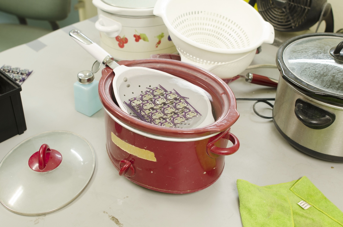
Don’t have access to an expensive washer? A cheap crockpot with deionized water and a toothbrush work swimmingly! If you’re cleaning just a few boards, a Q-tip with some isopropyl alcohol works very well.
A fan or compressed air work well to remove any water that remains.
Packaging
The board is reaching the end of its journey!
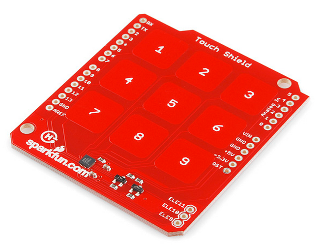
Once the batch of boards is clean and dry, they go to packaging where each board is individually heat sealed into ESD plastic.
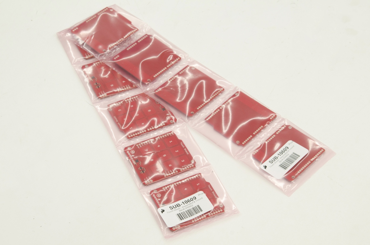
Because picking and packaging orders needs to be as fast as possible, we make sure every product is ‘pick ready’ for the shipping department. For most products, we will create a chain of 10 pieces with a bar-coded label on each end. The barcode label contains the product name, SKU, and a batch identifier that helps us track any problems.
Once the product is completely packaged, it is sent over to the shipping floor. We record the departing inventory, deduct all the work in progress parts, and add the new quantities to our storefront stock. The product then begins an entirely new journey to your door. We'll leave that tutorial for another day.
Resources and Going Further
Thanks for checking out how we build electronics at SparkFun. Now that you’ve read a little, we recommend you checkout a few more tutorials:
Or check out some of these blog posts related to production and manufacturing widgets at SparkFun!