Qwiic ToF Imager - VL53L5CX Hookup Guide
 Nate, Ell C
Hardware Overview
VL53L5CX
The SparkFun Qwiic ToF Imager and Qwiic ToF Mini are state of the art, 64 pixel Time-of-Flight (ToF) 4 meter ranging sensors built around the VL53L5CX from ST. To see more details, refer to the datasheet.
 |
 |
| Qwiic ToF Imager - VL53L5CX | Qwiic Mini ToF Imager - VL53L5CX |
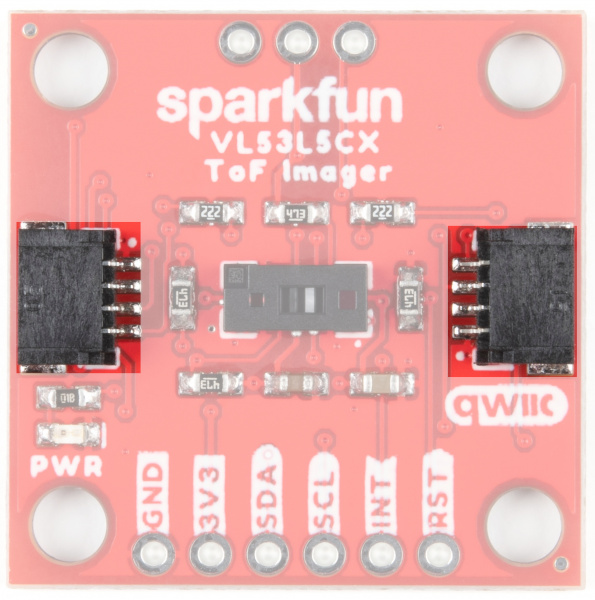
Qwiic Connectors
Our Qwiic Ecosystem makes sensors pretty much plug and play. There are two Qwiic connectors on either side of the Qwiic Air Velocity Sensor board to provide power and I2C connectivity simultaneously.
The 7-bit unshifted I2C address (most commonly used with Arduino) is 0x29. The 8-bit I2C address of the board is 0x52 for writing and 0x53 for reading.
 |
|
| Qwiic ToF Imager - VL53L5CX | Qwiic Mini ToF Imager - VL53L5CX |
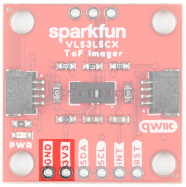
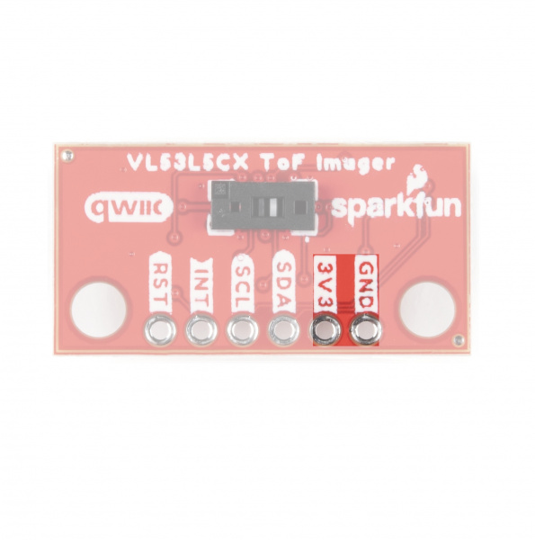
Power
Ideally power will be supplied by the Qwiic connector, but if you wish to supply your own power, pins have been broken out along the bottom side of the board labeled 3V3 and GND. The input voltage range should be between 2.7-3.3V.
 |
 |
| Qwiic ToF Imager - VL53L5CX | Qwiic Mini ToF Imager - VL53L5CX |
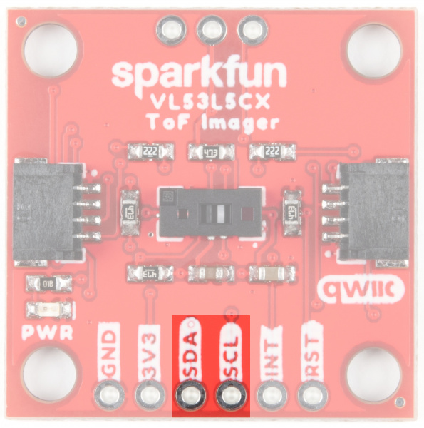
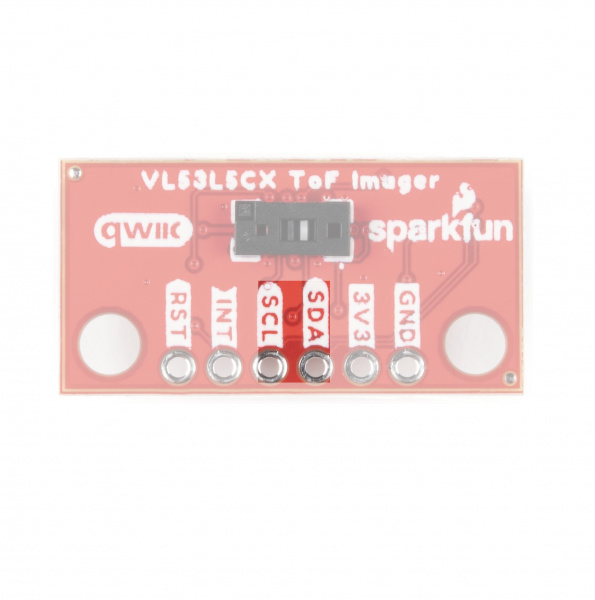
I2C
The I2C pins break out the functionality of the Qwiic connectors. Depending on your application, you can connect to these pins via the plated through holes for SDA and SCL.
 |
 |
| Qwiic ToF Imager - VL53L5CX | Qwiic Mini ToF Imager - VL53L5CX |
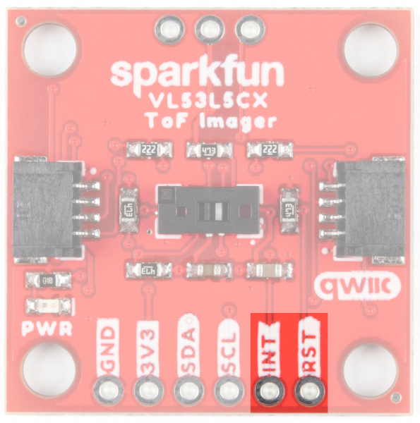
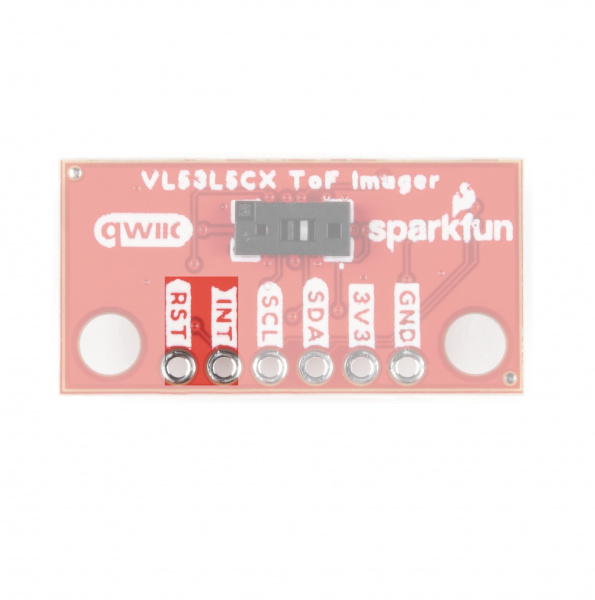
INT and RST
The interrupt pin is the interrupt output and defaults to an open-drain output. A 47 kΩ pull-up resistor to IOVDD is included.
The reset pin is the I2C interface reset pin and is active high. It is pulled to ground with a 47 kΩ resistor.
 |
 |
| Qwiic ToF Imager - VL53L5CX | Qwiic Mini ToF Imager - VL53L5CX |
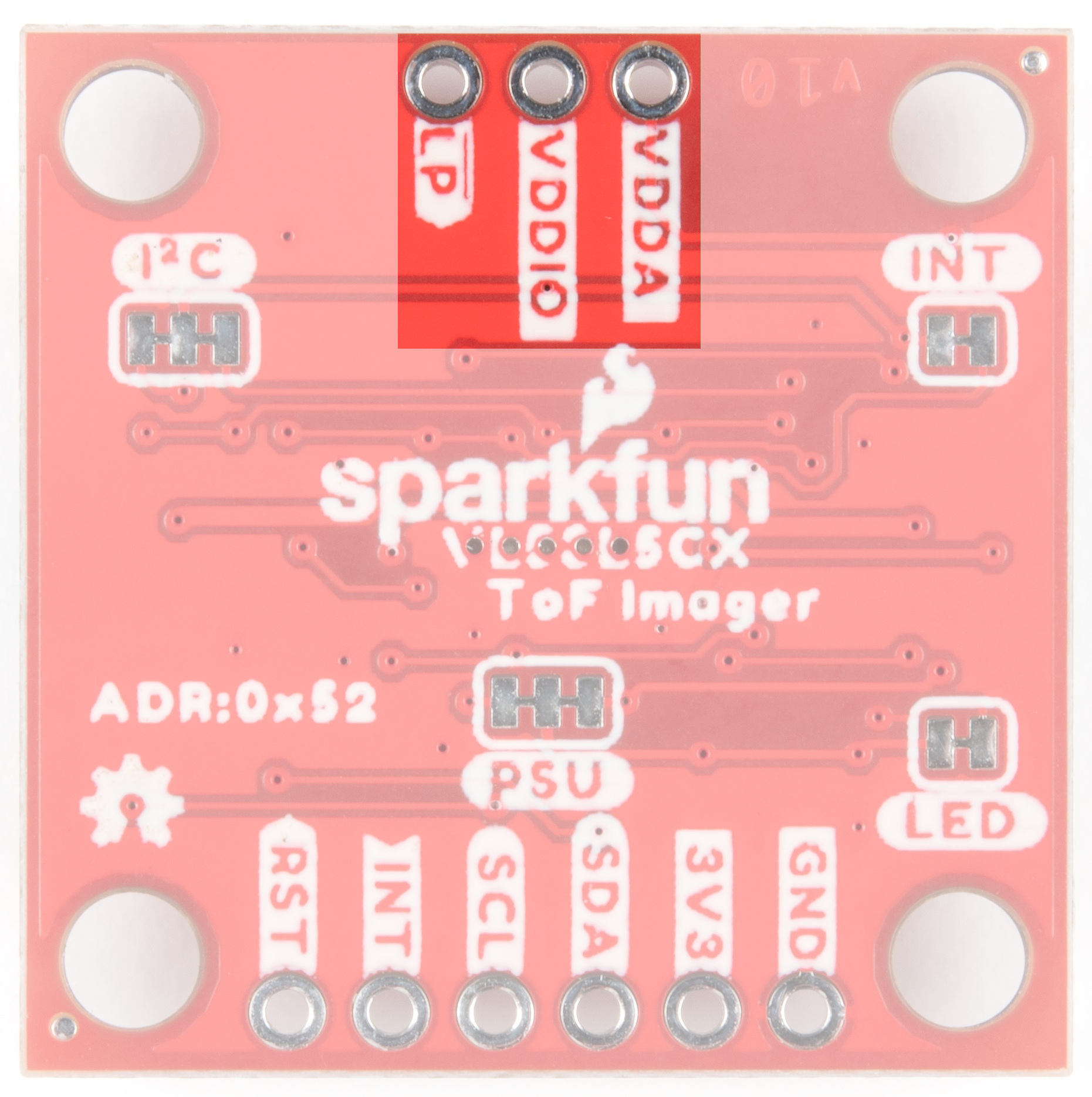
LP, VDDIO, & VDDA
The pins in this section are specific to the 1"x1" board. LP is a low power enable pin. Drive this pin to logic 0 to disable the I2C comms to reduce power consumption. Drive this pin to logic 1 to enable I2C comms. This pin is typically only needed when you need to change the I2C address in multidevice systems. A 47 kΩ pull-up resistor to IOVDD is included so it can be left unconnected.
VDDIO/VDDA: These pins are used as an alternate power supply. By default, VDDIO and VDDA are tied together but by opening the PSU jumper they can be isolated. A user must then provide separate VDDIO and VDDA supplies. This is most applicable for users who want to use IO voltages (1.8, 2.8, or 3.3V) separate from AVDD voltages (2.8 or 3.3V) for maximum power reduction.
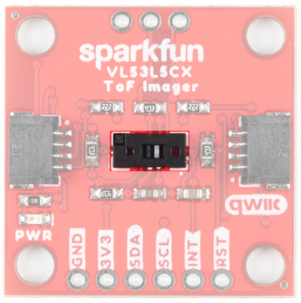
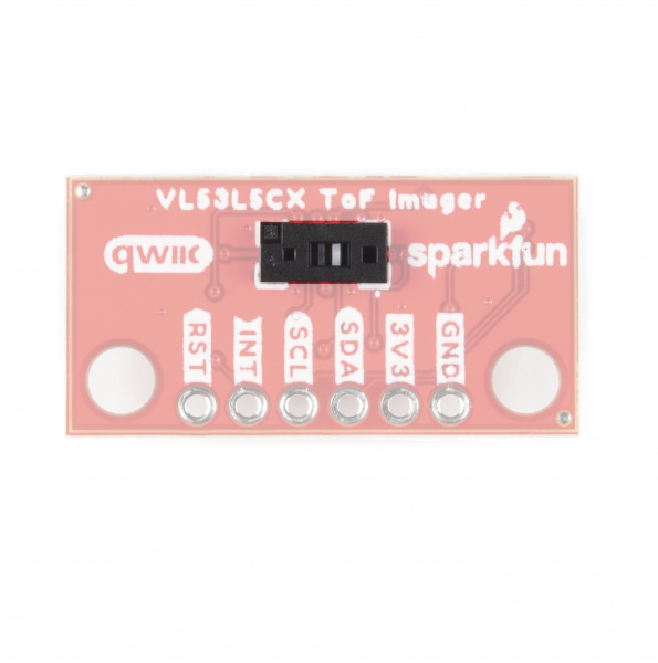
Jumpers
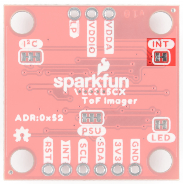
INT
Cut the INT jumper to remove the 47 kΩ pull-up resistor from the INT pin.
 |
 |
| Qwiic ToF Imager - VL53L5CX | Qwiic Mini ToF Imager - VL53L5CX |
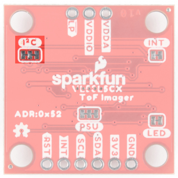
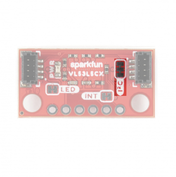
I2C
The SparkFun Qwiic ToF Imager Sensor has two 2.2 kΩ pull-up resistors attached to the I2C bus by default. If multiple sensors are connected to the bus with the pull-up resistors enabled the parallel equivalent resistance may create too strong of a pull-up for the bus to operate correctly. As a general rule of thumb, disable all but one pair of pull-up resistors if multiple devices are connected to the bus. If you need to disconnect the pull-up resistors they can be removed by cutting the traces on the corresponding jumper highlighted below.
 |
 |
| Qwiic ToF Imager - VL53L5CX | Qwiic Mini ToF Imager - VL53L5CX |
PSU
This jumper is related to the pins specific to the 1" x 1" ToF board. By default, VDDIO and VDDA are tied together. Cutting the PSU jumper will isolate the power rails. A user must then provide separate VDDIO and VDDA supplies. This is most applicable for users who want to use IO voltages (1.8, 2.8, or 3.3V) separate from AVDD voltages (2.8 or 3.3V) for maximum power reduction.

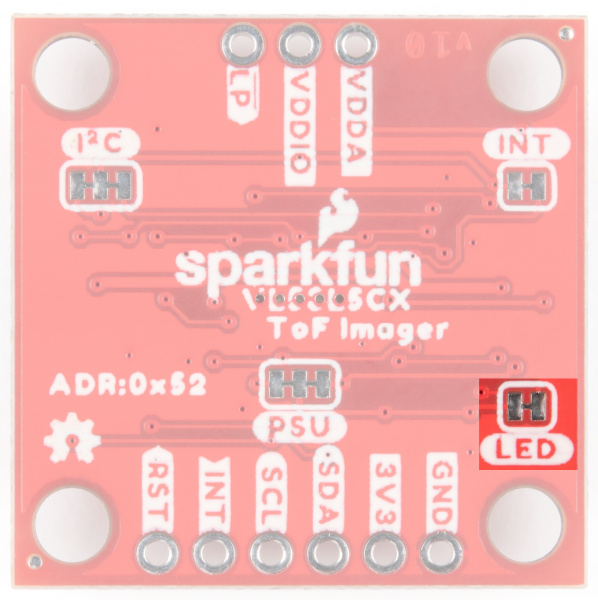
LED
If minimal power consumption is a concern, or you just don't want that Power LED on the front of the board to light up, go ahead and cut this jumper.
 |
 |
| Qwiic ToF Imager - VL53L5CX | Qwiic Mini ToF Imager - VL53L5CX |
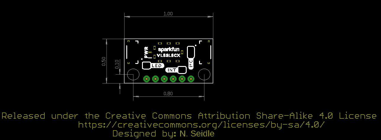
Board Outline
Qwiic ToF Imager - VL53L5CX
This sensor measures 1" x 1".

Qwiic Mini ToF Imager - VL53L5CX
This sensor measures 0.5" x 1".