Proto Pedal Example: Analog Equalizer Project
 Byron J.
Theory
The schematic breaks down into several functional blocks.
We're going to quickly cover them below. If you want much more detail, you can find it in this white paper.
Input Buffer
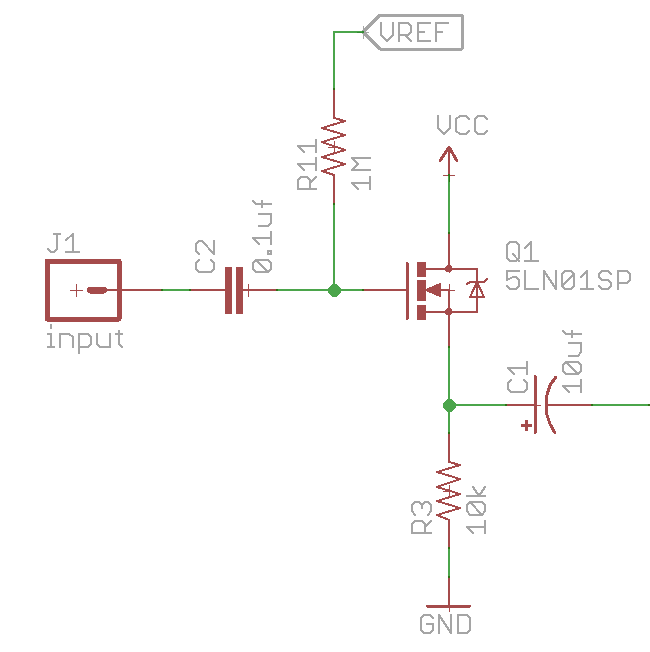
The start of our path through the equalizer is a single MOSFET, wired as a source follower. This bumps up the input impedance and prevents a loss of high frequencies when the pedal is switched on.
Because the input impedance is so high (defined by the parallel combination of R11 and the 1M input pull-down on the board, or 500 kΩ), the input coupling cap (C2) can be a very small value.
The buffer feeds into the...
Cut/Boost Amplifier
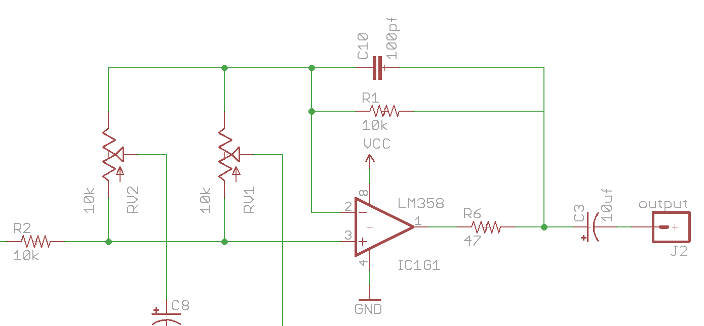
This amplifier is the heart of the equalizer circuit. It's configured as a unity gain noninverting amplifier. The gyrator circuits (more below!) are attached to potentiometers that "swing" between the inverting and non-inverting inputs of this op-amp. This EQ curcuit is sometimes called the "swinging input" topology.
Gyrators
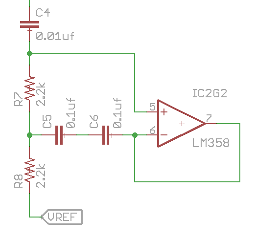
A gyrator is a virtual inductor, made with a capacitor and an op-amp. By putting a second capacitor in series with the gyrator, a band-stop filter is created.
Since we're using the decade-value capacitors from the capacitor kit, we're taking advantage of the series combination of some of the caps to get different values, as implemented with C7-C8 and C5-C6.
These band stop filters are attached to potentiometers that move them between the inverting and non-inverting inputs of the cut/boost amplifier.
When the bandstop filter is on the + input, that band is removed from the input signal, resulting in a cut. When it's on the - input, it's removing the frequency from the feedback path. The result of cutting the feedback is a boost at the frequency. When the potentiometers are in the middle, the cut and boost actions balance each other, with no net change.
Buffered Half-Rail
Finally, part of the circuit serves as an ancillary power supply.
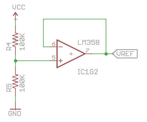
The circuit requires three op-amps, but with two dual op-amp chips, we have a spare. That extra amplifier is configured as a voltage follower on a half-rail voltage. It's used for the DC bias added to the signal and also as the "virtual ground" that the gyrators dump signal into.
Many pedals use pairs of equal value resistors as dividers, to create Vcc/2 reference voltages. By buffering a single divider with an op-amp, we have a half-rail of lower impedance. It costs an op-amp stage (that was otherwise unused) but probably saves a number of resistors.
The half rail is treated as VAUX, applied to one of the lateral traces in the center of the breadboard.