MicroMod ESP32 Processor Board Hookup Guide
 Alex the Giant, Ell C
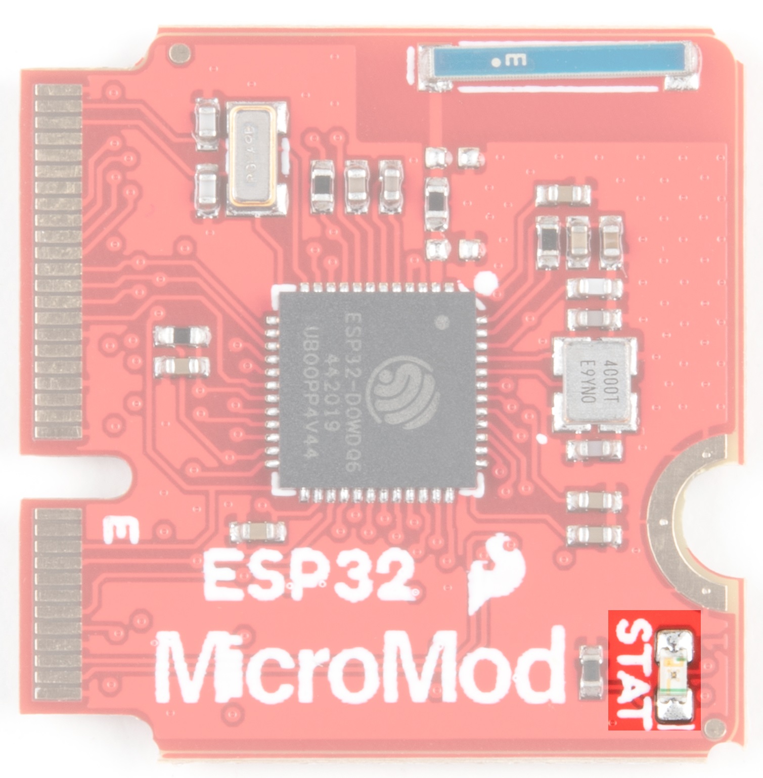
Hardware Overview
In this section we'll cover what's included on the MicroMod ESP32 Processor Board.
M.2 Connector
All of our MicroMod Processor boards come equipped with the M.2 MicroMod Connector, which leverages the M.2 standard and specification to allow you to install your MicroMod Processor board on your choice of carrier board.
 |
 |
| M2 Connector from the Front | M2 Connector from the Back |
Espressif ESP32
Ahhh, the Espressif ESP32. It's one of the most unique microcontrollers on the market. In it's native form, it has a laundry list of features. On the MicroMod Processor Board, we include the following:
- Dual-core Tensilica LX6 microprocessor
- Up to 240MHz clock frequency
- 520kB internal SRAM
- Integrated 802.11 B/G/N WiFi transceiver
- 2.7 to 3.6V operating range
- 10-electrode capacitive touch support
- Hardware accelerated encryption (AES, SHA2, ECC, RSA-4096)
- 16MB Flash Storage

Stat LED
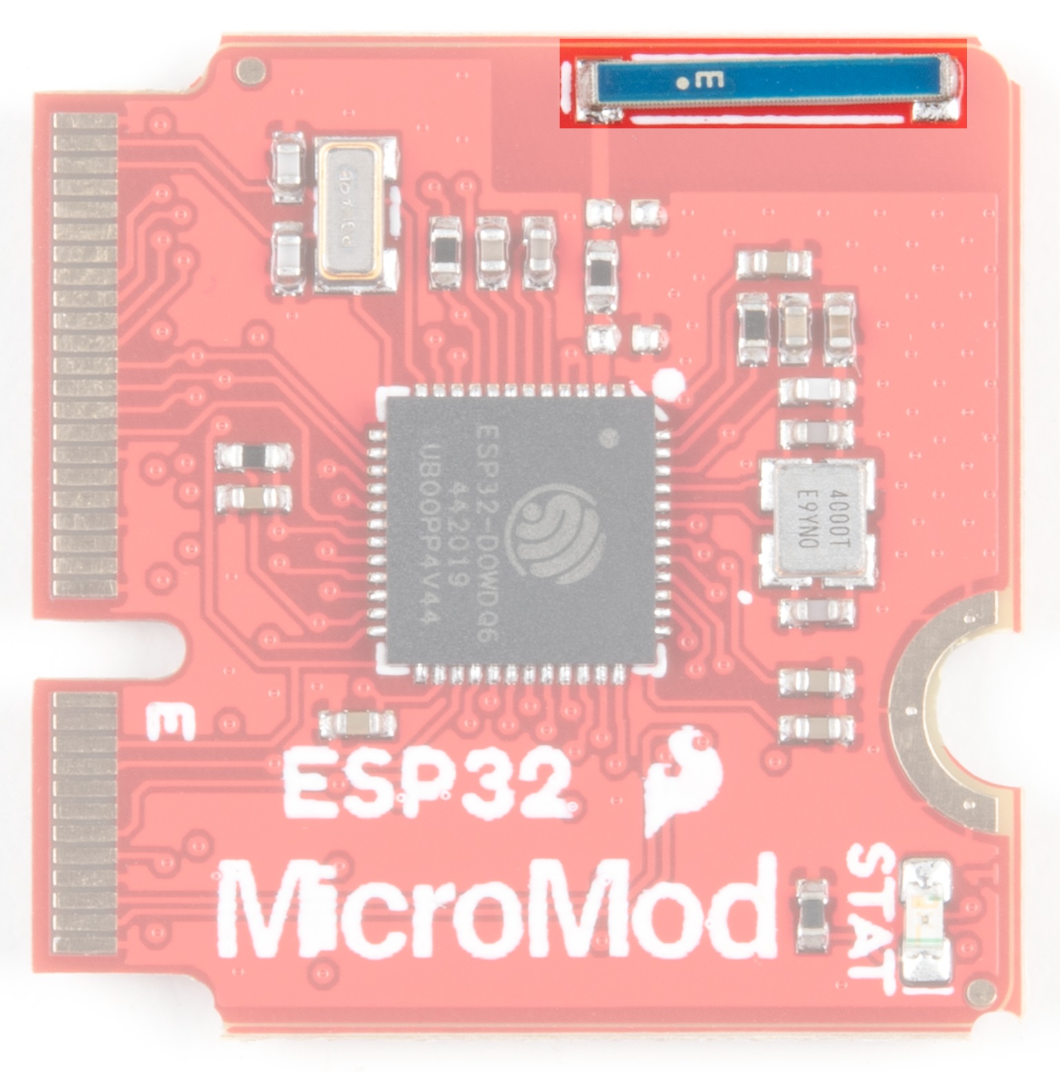
Wireless Antenna
Need wireless? The Espressif chip provides a WiFi transceiver which sends and receives data through a 2.4GHz Antenna.
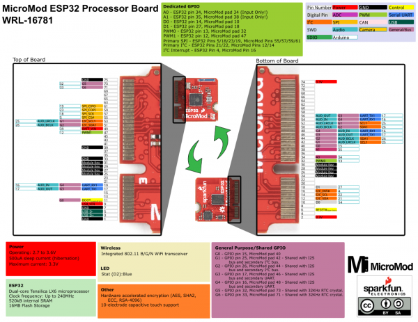
PinOut Notes
The ESP32 MicroMod has a few quirks. The ESP32's GPIO pins provide a lot of flexibility with what each pin can be used for. Whether it's I2C, I2S, SPI, UART, or PWM, the ESP32 MicroMod can do just about everything! However, with that flexibility and a fixed number of GPIO pins, the ESP32 isn't able to do it all at the same time. Below is a list of protocols the ESP32 supports, but pay close attention to the pins used, because some pins are assigned to two or possibly three functions.
Strapping Pins
One of the unique aspects of the ESP32 is the strapping pins. When the ESP32 comes out of reset, or as power is supplied, there are a few pins which control the behavior of the board. For a detailed description of these pins, check out the ESP32 Boot Mode Selection page on espressif's GitHub page. As a summary the strapping pins are:
GPIO 0
Having GPIO 0 pulled low as the ESP32 comes out of reset will enter the serial bootloader. Otherwise, the board will run the program stored in flash. On the MicroMod Processor, this pin is pulled high externally through a 10k resistor, and is connected to the boot button on the carrier boards, which can pull the pin low.
GPIO 2
Having GPIO 2 pulled high as the ESP32 comes out of reset will prevent the board from entering the serial bootloader. On the MicroMod Processor, this pin is connected to the status LED (active high) and does not interfere with the board from being able to enter the serial bootloader.
GPIO 12
If driven high, the flash voltage (VDD_SDIO) is set to 1.8V. If unconnected or pulled low, VDD_SDIO is set to 3.3V. The flash IC used on the MicroMod Processor has a minimum voltage of 2.7V, which would create a brownout condition and might corrupt the data stored to the flash, or simply prevent the program from running. On the ESP32 MicroMod Processor, this pin is connected to PWM1.
GPIO 15
If driven low, the boot messages printed by the ROM bootloader (at 115200 baud) are silenced. If unconnected or driven high, the messages will be printed as they normally are. On the ESP32 MicroMod Processor, this pin is connected to G0.
I2C
We love us some I2C! We've broken out two I2C buses, which can be used with our Qwiic system. The main I2C bus has dedicated GPIO pins 21/22 connected to MicroMod pads 12/14, along with a dedicated interrupt pin connected to GPIO pin 4, which is connected to pad 16 of the MicroMod connector.
If you need a second I2C bus, the ESP32 uses GPIO pins 25/26 (pads 42/44 on the MicroMod) for SCL1 and SDA1.
UART
The ESP32 Processor has two UARTs available. The primary UART has dedicated GPIO pins 1 and 3 which can be used for programming as well as printing debug messages to a terminal window. These GPIO pins aren't directly broken out, but instead are converted to USB which is connected to MicroMod pads 3 and 5.
The second UART is connected GPIO pins 16 and 17 (pads 19 and 17 on the MicroMod) for RX1 and TX1.
GPIO/BUS
The MicroMod connector supports a total of 12 general purpose IO pins, 7 of which are used on the ESP32 Processor, on top of the 6 dedicated pins. The dedicated pins are just that, and are not shared with any other pin, unlike the general purpose pins which may be shared with other pins. The pins used are:
Dedicated Pins
- A0 - GPIO pin 34, pad 34 on the MicroMod (Input Only!)
- A1 - GPIO pin 35, pad 38 on the MicroMod (Input Only!)
- D0 - GPIO pin 14, pad 10 on the MicroMod
- D1 - GPIO pin 27, pad 18 on the MicroMod
- PWM0 - GPIO pin 13, pad 32 on the MicroMod
- PWM1 - GPIO pin 12, pad 47 on the MicroMod
General Purpose IO pins
- G0 - GPIO pin 15, pad 40 on the MicroMod
- G1 - GPIO pin 25, pad 42 on the MicroMod - Shared with the I2S bus, and secondary I2C bus.
- G2 - GPIO pin 26, pad 44 on the MicroMod - Shared with the I2S bus, and secondary I2C bus.
- G3 - GPIO pin 17, pad 46 on the MicroMod - Shared with the I2S bus, and secondary UART.
- G4 - GPIO pin 16, pad 48 on the MicroMod - Shared with the I2S bus, and secondary UART.
- G5 - GPIO pin 32, pad 73 on the MicroMod - Shared with the 32KHz RTC crystal.
- G6 - GPIO pin 33, pad 71 on the MicroMod - Shared with the 32KHz RTC crystal.
AUDIO
The ESP32 Processor supports audio using the I2S standard. The pins used are:
- AUD_OUT - GPIO pin 17, pad 56 on the MicroMod, this is the digital audio output.
- AUD_IN - GPIO pin 16, pad 54 on the MicroMod, this is the digital audio input.
- AUD_LRCLK - GPIO pin 25, pad 52 on the MicroMod. Officially called "word select", and also known as "frame sync".
- AUD_BCLK - GPIO pin 26, pad 50 on the MicroMod. Offically called "continuous serial clock, and also known as the "bit clock"
SPI
The MicroMod standard supports two Serial Peripheral Interface (SPI) buses, but because of the limited GPIO pins here, only the primary SPI bus is used. This primary SPI bus is dedicated to the following pins:
- SCK - This is the clock pin, which is connected to GPIO 18, or MicroMod pad 57.
- SDO - This is the serial data output of the ESP32, which is connected to GPIO 23, or MicroMod pad 59.
- SDI - This is the serial data input of the ESP32, which is connected to GPIO 19, or MicroMod pad 61.
- #CS - This is the chip select pin, which is connected to GPIO 5, or MicroMod pad 55.
ESP32 MicroMod Processor Pin Functionality
| AUDIO | UART | GPIO/BUS | I2C | SDIO | SPI0 | Dedicated |
| Function | Bottom Pin |
Top Pin |
Function | ||||||
|---|---|---|---|---|---|---|---|---|---|
| (Not Connected) | 75 | GND | |||||||
| 3.3V | 74 | 73 | G5 / BUS5 | ||||||
| RTC_3V_BATT | 72 | 71 | G6 / BUS6 | ||||||
| SPI_CS1# | SDIO_DATA3 (I/O) | 70 | 69 | G7 / BUS7 | |||||
| SDIO_DATA2 (I/O) | 68 | 67 | G8 | ||||||
| SDIO_DATA1 (I/O) | 66 | 65 | G9 | ADC_D- | CAM_HSYNC | ||||
| SPI_CIPO1 | SDIO_DATA0 (I/O) | 64 | 63 | G10 | ADC_D+ | CAM_VSYNC | |||
| SPI COPI1 | SDIO_CMD (I/O) | 62 | 61 | SPI_CIPO (I) | |||||
| SPI SCK1 | SDIO_SCK (O) | 60 | 59 | SPI_COPI (O) | LED_DAT | ||||
| AUD_MCLK (O) | 58 | 57 | SPI_SCK (O) | LED_CLK | |||||
| CAM_MCLK | PCM_OUT | I2S_OUT | AUD_OUT | 56 | 55 | SPI_CS# | |||
| CAM_PCLK | PCM_IN | I2S_IN | AUD_IN | 54 | 53 | I2C_SCL1 (I/O) | |||
| PDM_DATA | PCM_SYNC | I2S_WS | AUD_LRCLK | 52 | 51 | I2C_SDA1 (I/O) | |||
| PDM_CLK | PCM_CLK | I2S_SCK | AUD_BCLK | 50 | 49 | BATT_VIN / 3 (I - ADC) (0 to 3.3V) | |||
| G4 / BUS4 | 48 | 47 | PWM1 | ||||||
| G3 / BUS3 | 46 | 45 | GND | ||||||
| G2 / BUS2 | 44 | 43 | CAN_TX | ||||||
| G1 / BUS1 | 42 | 41 | CAN_RX | ||||||
| G0 / BUS0 | 40 | 39 | GND | ||||||
| A1 | 38 | 37 | USBHOST_D- | ||||||
| GND | 36 | 35 | USBHOST_D+ | ||||||
| A0 | 34 | 33 | GND | ||||||
| PWM0 | 32 | 31 | Module Key | ||||||
| Module Key | 30 | 29 | Module Key | ||||||
| Module Key | 28 | 27 | Module Key | ||||||
| Module Key | 26 | 25 | Module Key | ||||||
| Module Key | 24 | 23 | SWDIO | ||||||
| UART_TX2 (O) | 22 | 21 | SWDCK | ||||||
| UART_RX2 (I) | 20 | 19 | UART_RX1 (I) | ||||||
| CAM_TRIG | D1 | 18 | 17 | UART_TX1 (0) | |||||
| I2C_INT# | 16 | 15 | UART_CTS1 (I) | ||||||
| I2C_SCL (I/0) | 14 | 13 | UART_RTS1 (O) | ||||||
| I2C_SDA (I/0) | 12 | 11 | BOOT (I - Open Drain) | ||||||
| D0 | 10 | 9 | USB_VIN | ||||||
| SWO | G11 | 8 | 7 | GND | |||||
| RESET# (I - Open Drain) | 6 | 5 | USB_D- | ||||||
| 3.3V_EN | 4 | 3 | USB_D+ | ||||||
| 3.3V | 2 | 1 | GND | ||||||
| ESP32 Pin | Alternate Function | Primary Function | Bottom Pin | Top Pin | Primary Function | Alternate Function | ESP32 Pin | ||
|---|---|---|---|---|---|---|---|---|---|
| 73 | G5 | RTC | 32 | ||||||
| 71 | G6 | RTC | 33 | ||||||
| 61 | SPI_CIPO | 19 | |||||||
| 59 | SPI_COPI | 23 | |||||||
| 57 | SPI_SCK | 18 | |||||||
| 17 | AUD_OUT | TX1 | G3 | 56 | 55 | SPI_CS# | 5 | ||
| 16 | AUD_IN | RX1 | G4 | 54 | 53 | SCL1 | G1 | AUD_LRCLK | 25 |
| 25 | AUD_LRCLK | SCL1 | G1 | 52 | 51 | SDA1 | G2 | AUD_BCLK | 26 |
| 26 | AUD_BCLK | SDA1 | G2 | 50 | 49 | BATT_VIN / 3 | 39 | ||
| 16 | AUD_IN | RX1 | G4 | 48 | 47 | PWM1 | 12 | ||
| 17 | AUD_OUT | TX1 | G3 | 46 | |||||
| 26 | AUD_BCLK | SDA1 | G2 | 44 | |||||
| 25 | AUD_LRCLK | SCL1 | G1 | 42 | |||||
| 15 | G0 | 40 | 39 | GND | |||||
| 35 | A1 | 38 | |||||||
| 34 | A0 | 34 | |||||||
| 13 | PWM0 | 32 | 33 | GND | |||||
| 19 | G4 | RX1 | AUD_IN | 16 | |||||
| 27 | CAM_TRIG | D1 | 18 | 17 | G3 | TX1 | AUD_OUT | 17 | |
| 4 | I2C Interrupt | 16 | |||||||
| 22 | SCL | 14 | |||||||
| 21 | SDA | 12 | 11 | BOOT | |||||
| 14 | D0 | 10 | 9 | USB_VIN | |||||
| 7 | GND | ||||||||
| RESET | 6 | 5 | USB_D- | ||||||
| 3 | USB_D+ | ||||||||
| 3.3V | 2 | 1 | GND | ||||||
| Signal Group | Signal | I/O | Description | Voltage | Power | 3.3V | I | 3.3V Source | 3.3V |
|---|---|---|---|---|
| GND | Return current path | 0V | ||
| USB_VIN | I | USB VIN compliant to USB 2.0 specification. Connect to pins on processor board that require 5V for USB functionality | 4.8-5.2V | |
| RTC_3V_BATT | I | 3V provided by external coin cell or mini battery. Max draw=100μA. Connect to pins maintaining an RTC during power loss. Can be left NC. | 3V | |
| 3.3V_EN | O | Controls the carrier board's main voltage regulator. Voltage above 1V will enable 3.3V power path. | 3.3V | |
| BATT_VIN/3 | I | Carrier board raw voltage over 3. 1/3 resistor divider is implemented on carrier board. Amplify the analog signal as needed for full 0-3.3V range | 3.3V | |
| Reset | Reset | I | Input to processor. Open drain with pullup on processor board. Pulling low resets processor. | 3.3V |
| Boot | I | Input to processor. Open drain with pullup on processor board. Pulling low puts processor into special boot mode. Can be left NC. | 3.3V | |
| USB | USB_D± | I/O | USB Data ±. Differential serial data interface compliant to USB 2.0 specification. If UART is required for programming, USB± must be routed to a USB-to-serial conversion IC on the processor board. | |
| USB Host | USBHOST_D± | I/O | For processors that support USB Host Mode. USB Data±. Differential serial data interface compliant to USB 2.0 specification. Can be left NC. | |
| CAN | CAN_RX | I | CAN Bus receive data. | 3.3V |
| CAN_TX | O | CAN Bus transmit data. | 3.3V | |
| UART | UART_RX1 | I | UART receive data. | 3.3V |
| UART_TX1 | O | UART transmit data. | 3.3V | |
| UART_RTS1 | O | UART ready to send. | 3.3V | |
| UART_CTS1 | I | UART clear to send. | 3.3V | |
| UART_RX2 | I | 2nd UART receive data. | 3.3V | |
| UART_TX2 | O | 2nd UART transmit data. | 3.3V | |
| I2C | I2C_SCL | I/O | I2C clock. Open drain with pullup on carrier board. | 3.3V |
| I2C_SDA | I/O | I2C data. Open drain with pullup on carrier board | 3.3V | |
| I2C_INT# | I | Interrupt notification from carrier board to processor. Open drain with pullup on carrier board. Active LOW | 3.3V | |
| I2C_SCL1 | I/O | 2nd I2C clock. Open drain with pullup on carrier board. | 3.3V | |
| I2C_SDA1 | I/O | 2nd I2C data. Open drain with pullup on carrier board. | 3.3V | |
| SPI | SPI_COPI | O | SPI Controller Output/Peripheral Input. | 3.3V |
| SPI_CIPO | I | SPI Controller Input/Peripheral Output. | 3.3V | |
| SPI_SCK | O | SPI Clock. | 3.3V | |
| SPI_CS# | O | SPI Chip Select. Active LOW. Can be routed to GPIO if hardware CS is unused. | 3.3V | |
| SPI/SDIO | SPI_SCK1/SDIO_CLK | O | 2nd SPI Clock. Secondary use is SDIO Clock. | 3.3V |
| SPI_COPI1/SDIO_CMD | I/O | 2nd SPI Controller Output/Peripheral Input. Secondary use is SDIO command interface. | 3.3V | |
| SPI_CIPO1/SDIO_DATA0 | I/O | 2nd SPI Peripheral Input/Controller Output. Secondary use is SDIO data exchange bit 0. | 3.3V | |
| SDIO_DATA1 | I/O | SDIO data exchange bit 1. | 3.3V | |
| SDIO_DATA2 | I/O | SDIO data exchange bit 2. | 3.3V | |
| SPI_CS1/SDIO_DATA3 | I/O | 2nd SPI Chip Select. Secondary use is SDIO data exchange bit 3. | 3.3V | |
| Audio | AUD_MCLK | O | Audio master clock. | 3.3V |
| AUD_OUT/PCM_OUT/I2S_OUT/CAM_MCLK | O | Audio data output. PCM synchronous data output. I2S serial data out. Camera master clock. | 3.3V | |
| AUD_IN/PCM_IN/I2S_IN/CAM_PCLK | I | Audio data input. PCM syncrhonous data input. I2S serial data in. Camera periphperal clock. | 3.3V | |
| AUD_LRCLK/PCM_SYNC/I2S_WS/PDM_DATA | I/O | Audio left/right clock. PCM syncrhonous data SYNC. I2S word select. PDM data. | 3.3V | |
| AUD_BCLK/PCM_CLK/I2S_CLK/PDM_CLK | O | Audio bit clock. PCM clock. I2S continuous serial clock. PDM clock. | 3.3V | |
| SWD | SWDIO | I/O | Serial Wire Debug I/O. Connect if processor board supports SWD. Can be left NC. | 3.3V |
| SWDCK | I | Serial Wire Debug clock. Connect if processor board supports SWD. Can be left NC. | 3.3V | |
| ADC | A0 | I | Analog to digital converter 0. Amplify the analog signal as needed to enable full 0-3.3V range. | 3.3V |
| A1 | I | Analog to digital converter 1. Amplify the analog signal as needed to enable full 0-3.3V range. | 3.3V | |
| PWM | PWM0 | O | Pulse width modulated output 0. | 3.3V |
| PWM1 | O | Pulse width modulated output 1. | 3.3V | |
| Digital | D0 | I/O | General digital input/output pin. | 3.3V |
| D1/CAM_TRIG | I/O | General digital input/output pin. Camera trigger. | 3.3V | |
| General/Bus | G0/BUS0 | I/O | General purpose pins. Any unused processor pins should be assigned to Gx with ADC + PWM capable pins given priority (0, 1, 2, etc.) positions. The intent is to guarantee PWM, ADC and Digital Pin functionality on respective ADC/PWM/Digital pins. Gx pins do not guarantee ADC/PWM function. Alternative use is pins can support a fast read/write 8-bit or 4-bit wide bus. | 3.3V |
| G1/BUS1 | I/O | 3.3V | ||
| G2/BUS2 | I/O | 3.3V | ||
| G3/BUS3 | I/O | 3.3V | ||
| G4/BUS4 | I/O | 3.3V | ||
| G5/BUS5 | I/O | 3.3V | ||
| G6/BUS6 | I/O | 3.3V | ||
| G7/BUS7 | I/O | 3.3V | ||
| G8 | I/O | General purpose pin | 3.3V | |
| G9/ADC_D-/CAM_HSYNC | I/O | Differential ADC input if available. Camera horizontal sync. | 3.3V | |
| G10/ADC_D+/CAM_VSYNC | I/O | Differential ADC input if available. Camera vertical sync. | 3.3V | |
| G11/SWO | I/O | General purpose pin. Serial Wire Output | 3.3V |
Board Dimensions
The board measures 22mm x 22mm, with 15mm to the top notch and 12mm to the E key. For more information regarding the processor board physical standards, head on over to the Getting Started with MicroMod tutorial and check out the Hardware Overview section.
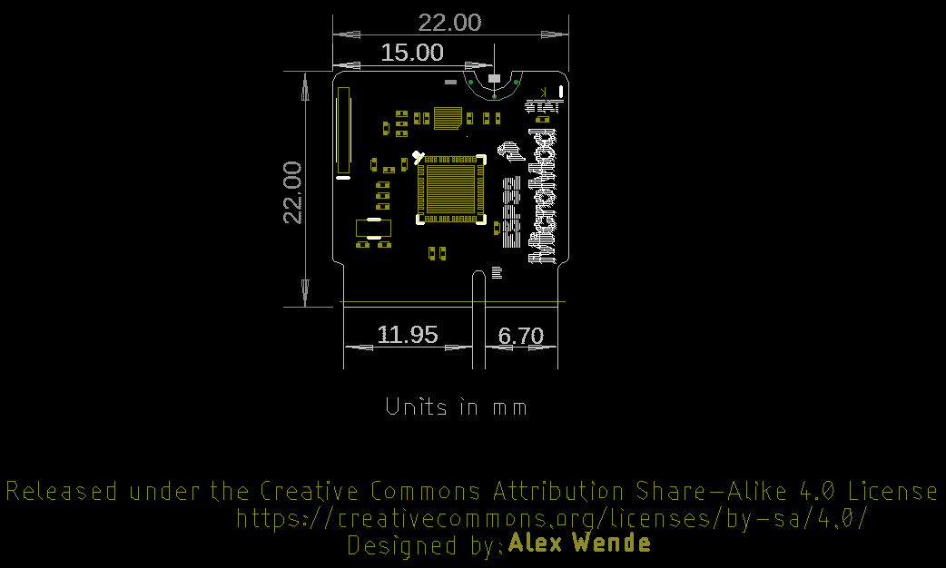
The overall thickness of the MicroMod ESP32 Processor Board is ~2.67mm. The height of the tallest component (ESP32 labeled as "U2" in the board file) on the Processor side is ~0.90mm. The PCB thickness is ~0.80mm. The height of the tallest component (transistor labeled as "Q2" in the board file) is about ~0.97mm.