SparkFun expLoRaBLE Hookup Guide
 QCPete, santaimpersonator
 Hardware Overview
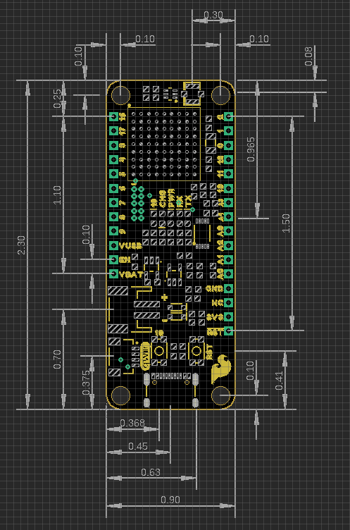
Board Dimensions
The board dimensions are illustrated in the drawing below. The listed measurements are in inches and the four mounting holes are compatible with 4-40 standoff screws.
USB-C Connector
The USB connector is provided to power and program the board. For most users, it will be the primary programing interface for the NM180100.

CH340E Serial-to-UART
The CH340E allows the NM180100 to communicate with a computer/host device through its USB-C connection. This allows the board to show up as a device on the serial (or COM) port of the computer. Users will need to install the latest CH340 driver for the computer to recognize the board.
How to Install CH340 Drivers
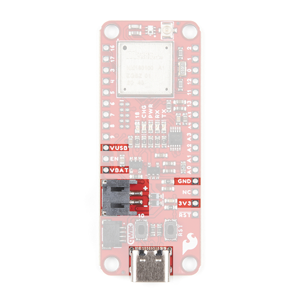
Power
The SparkFun expLoRaBLE only requires 3.3V to power the board. However, the simplest method to power the board is with the USB-C connector. There are additional power pins available on the board:
- 3.3V - A regulated 3.3V voltage source.
- Regulated from the USB 5V power and/or battery connection.
- Used to power the NM180100 SiP and Qwiic I2C bus.
- USB - The voltage from the USB-C connector, usually 5V.
- VBAT - The voltage from the JST battery connector; meant for single cell LiPo batteries.
- GND - The common ground or the 0V reference for the voltage supplies.
Charging Circuit
The charging circuit utilizes the MCP73831 linear charge management controller and is powered directly from the USB-C connector or USB. The controller is configured for a 500mA charge rate and battery charging is indicated when the yellow, CHG LED. If the charge controller is shutdown or charging is complete, the CHG LED will turn off. For more information, please refer to the MCP73831 datasheet.
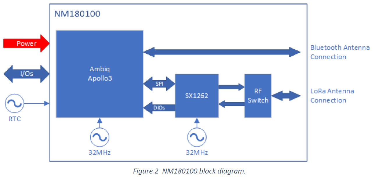
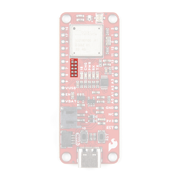
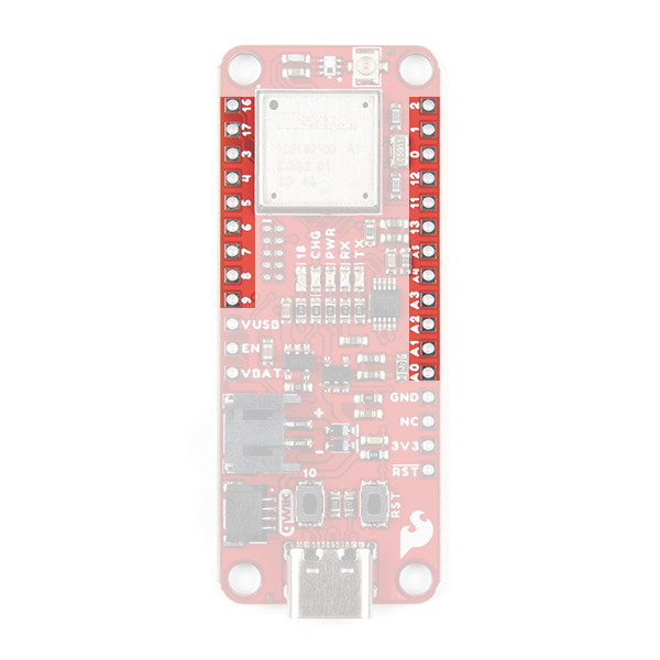
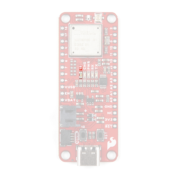
NM180100 SiP
The NM180100 SiP from Northern Mechatronics is the brains of the SparkFun expLoRaBLE. The system in package (SiP) includes an Apollo3 MCU connected to a Semtech SX1262 radio transceiver. The connection between the two ICs is laid out in the table below.
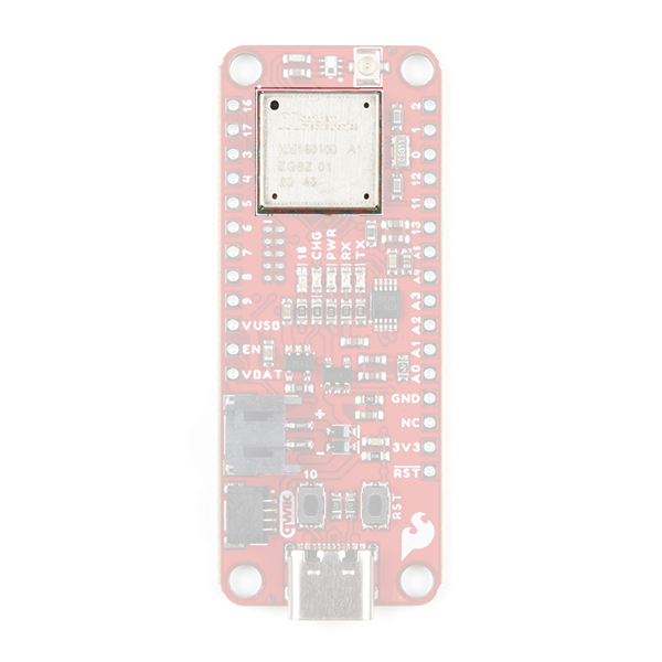
NM180100 SiP on the SparkFun expLoRaBLE. (Click to enlarge)
| Apollo3 | SX1262 | Description | ||
|---|---|---|---|---|
| Pin | Name | Pin | Name | |
| H6 | GPIO 36 | 19 | NSS | SPI Slave Select |
| J6 | GPIO 38 | 17 | MOSI | SPI Slave Input |
| J5 | GPIO 43 | 16 | MISO | SPI Slave Output |
| H5 | GPIO 42 | 18 | SCK | SPI Clock Input |
| J8 | GPIO 39 | 14 | Busy | Radio Busy Indicator |
| J9 | GPIO 40 | 13 | DIO1 | Multipurpose Digital I/o |
| H9 | GPIO 47 | 06 | DIO3 | Multipurpose Digital I/o |
| J7 | GPIO 44 | 15 | NRESET | Radio Reset Signal (Active Low) |
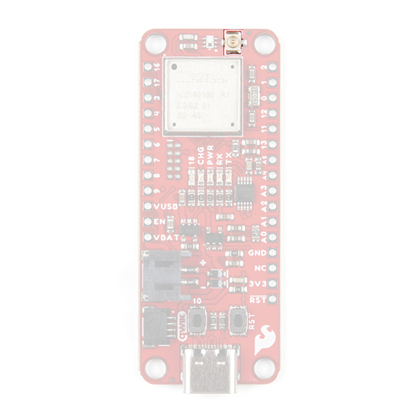
A breakdown of the NM180100 functionality is shown in the block diagram below and the functionality of each embedded chip is laid out in the following subsections. It should be noted, that the Bluetooth and LoRa antenna connections on the SparkFun expLoRaBLE share the same u.FL connector with the use of a diplexer. For more details on the NM180100 SiP, check out the datasheet.
Note: While most users will utilize the USB connection for serial programming, the Apollo3 MCU in the NM180100 SiP can also be programmed through its JTAG or SWD pins. This might is useful for individuals developing and testing firmware that would be flashed directly onto the NM180100 SiP, such as in production for commercial applications. For more details on programming, please check out our ARM Programming tutorial
ARM Programming
The JTAG pins on the SparkFun expLoRaBLE. (Click to enlarge)
Apollo3 MCU
For details on the Apollo3, users should refer to the Designing with the SparkFun Artemis hookup guide. Additionally, users can reference the following resources for more technical information:
Designing with the SparkFun Artemis
Hardware Information:
Development Platforms:
SX1262 RF Transceiver
The Semtech SX1262 module is a long range, low power, half-duplex transceiver with global LoRa® frequency coverage, capable of operating as a Long range (LoRa) wide area network (LoRaWAN) or frequency-shift keying (FSK) modem. The module was designed for long battery life with just 4.2 mA of active receive current consumption and it can transmit up to +22 dBm with the use of its highly efficient, integrated power amplifiers. The SX1262 is optimal for devices that are designed to comply with the physical layer requirements of the LoRaWAN specification released by the LoRa Alliance™. For more details on the SX1262, check out the datasheet.
Functional block diagram for the SX1262. (Click to enlarge)
| Characteristic | Description |
|---|---|
|
Current Consumption |
4.2 to 10.1 mA (RX) 32 to 118 mA (TX) |
| Frequency Range | 150 to 960 MHz |
| Modulation |
FSK, GFSK, MSK, GMSK and LoRa |
| Link Budget | 170 dB (max) |
|
Bit Rate (programmable) |
FSK: .6 to 300 kb/s LoRa: .018 to 62.5 kb/s |
| RF Sensitivity | -104 to -148 dBm |
| RF Output Power | +14 to +22 dBm |
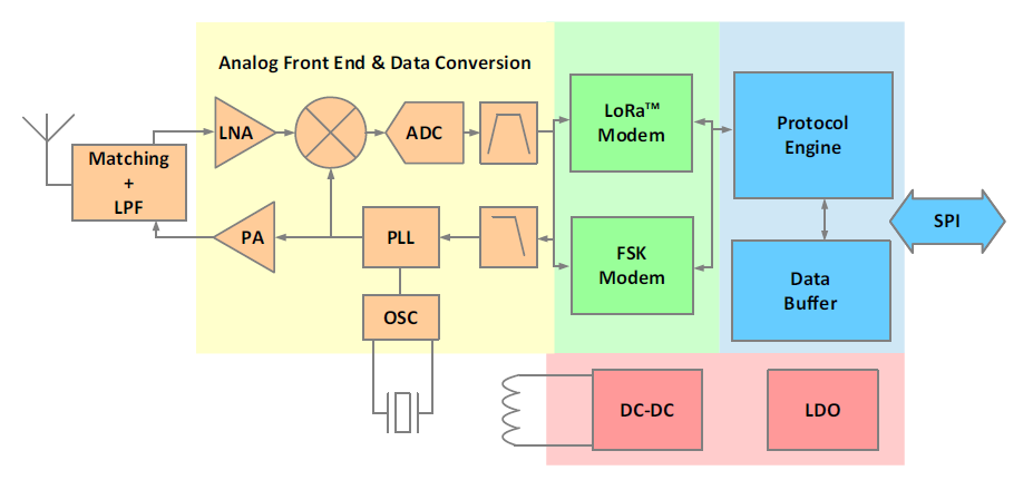
u.FL Antenna Connector
The Apollo3 BLE and SX1262 RF antenna connections share a single U.FL antenna connector with the use of a diplexer.
Breakout Pin Connections
The pins from the NM180100 SiP are broken out into a feather form factor layout.

Power Pins
The power pins aren't really I/O (Input/Output) connections for the microcontroller; however, they are pertinent to the board.
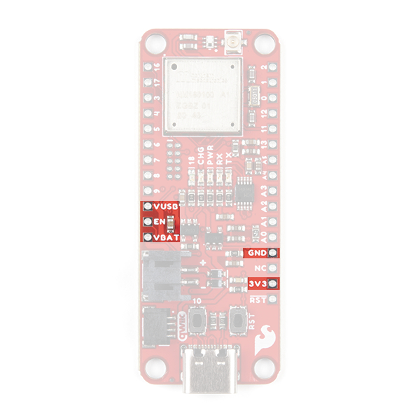
The power I/O mostly consists of voltage supply pins. These pins are traditionally used as power sources for other pieces of hardware (like LEDs, potentiometers, and other circuits).
- 3.3V - A regulated 3.3V voltage source.
- Regulated from the USB 5V power and/or battery connection.
- Used to power the NM180100 SiP and Qwiic I2C bus.
- USB - The voltage from the USB-C connector, usually 5V.
- VBAT - The voltage from the JST battery connector; meant for single cell LiPo batteries.
- GND - The common ground or the 0V reference for the voltage supplies.
EN pin is used to contol the 3.3V voltage regulator output (i.e. the boards power) from the battery or USB connection to the rest of the board.I/O Pins
There are 21 I/O pins broken out on this board, which can be used as digital inputs to or outputs from the NM180100 SiP.
All of the SparkFun expLoRaBLE pins are broken out with .1" pitch spacing for headers. It is best practice to define the pinMode() (link) in the setup of each sketch (programs written in the Arduino IDE) for the pins used.
Input
When configured properly, an input pin will be looking for a HIGH or LOW state. Input pins are High Impedance and takes very little current to move the input pin from one state to another.
Output
When configured as an output the pin will be at a HIGH or LOW voltage. Output pins are Low Impedance: This means that they can provide a relatively substantial amount of current to other circuits.
Additional Functions
There are several pins that have special functionality in addition to general digital I/O. These pins and their additional functions are listed in the tabs below. For more technical specifications on the I/O pins, you can refer to the Apollo 3 datasheet.
Analog Input Pins
Note: Be aware that the ADC input range is from 0 - 2V. Although connecting a sensor with an output to 3.3V is safe for the NM180100 SiP, it will saturate the ADC at 2V.
The NM180100 SiP offers a 14-bit ADC input for eight of the SparkFun expLoRaBLE's I/O pins. This functionality is accessed in the Arduino IDE using the analogRead(pin) function.
analogRead() returns a 10-bit value. To change the resolution of the value returned by the analogRead() function, use the analogReadResolution(bits) function.
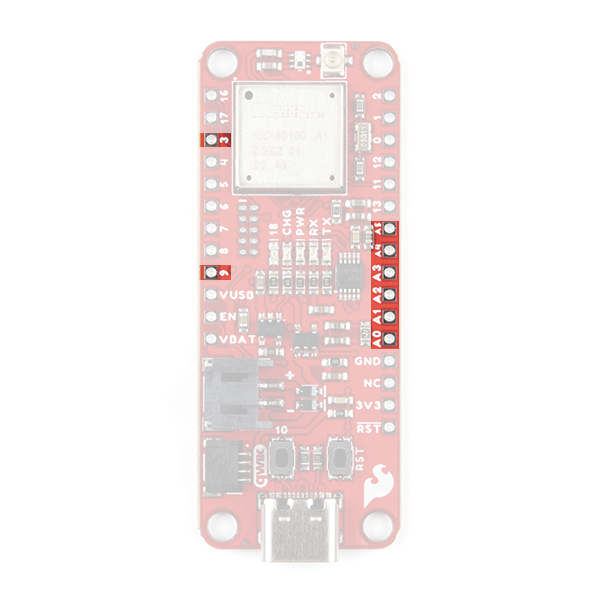
Analog input pins on the SparkFun expLoRaBLE. (Click to enlarge)
Note: To learn more about analog vs. digital signals, check out this great tutorial.
Analog vs. Digital
Pulse Width Modulation (PWM) Output Pins
The NM180100 SiP provides 16-bit PWM output for all of the SparkFun expLoRaBLE's twenty-one digital I/O pins. Additionally, the SCL line of the primary, Qwiic I2C bus and GPIO 10, which is connected to the status LED are also PWM capable outputs. This functionality is accessed in the Arduino IDE using the analogWrite(pin, value) function or the Servo library.
Note: By default, in the Arduino IDE, analogWrite() accepts an 8-bit value. To change the resolution of the PWM signal for the analogWrite() function, use the analogWriteResolution(bits) function.
(*The PWM output is the result of the NM180100 SiP's signal generator clock functionality and is not a true analog signal.)
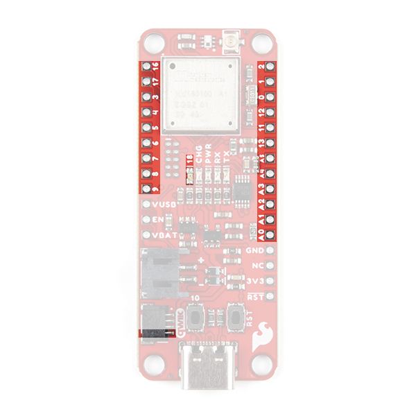
PWM pins on the SparkFun expLoRaBLE. (Click to enlarge)
Note: To learn more about pulse width modulation (PWM), check out this great tutorial.
Pulse Width Modulation
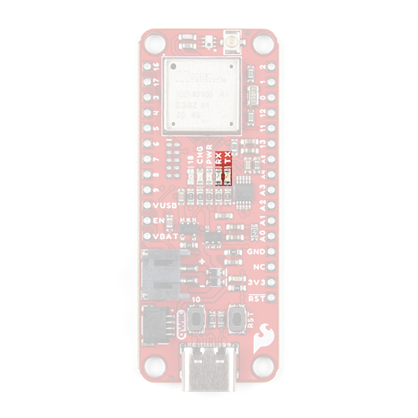
Serial Communication Pins
The SparkFun expLoRaBLE has two UART modules that can function independently of each other. By default, the dedicated UART port to the USB connection (Serial) can be accessed through the Arduino IDE using the serial communication module. D0 (RX) and D1 (TX) of the breakout I/O pins are connected to the secondary UART module.
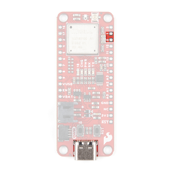
The available serial communication connections on the SparkFun expLoRaBLE.
Note: To learn more about serial communication, check out this great tutorial.
Serial Communication
SPI Communication
The default SPI bus on the SparkFun expLoRaBLE is accessible through the Arduino IDE using the SPI module. By default, in the Arduino IDE, the SPI module is configured to utilize pins 25, 27, and 28.
| Connection | Pin |
|---|---|
| SCK | 13 |
| SDI or CIPO | 12 |
| SDO or COPI | 11 |
| CS | ANY |
MOSI signal on a controller has been replaced with the title SDO. Please refer to this announcement on the decision to deprecate the MOSI/MISO terminology and transition to the SDO/SDI naming convention.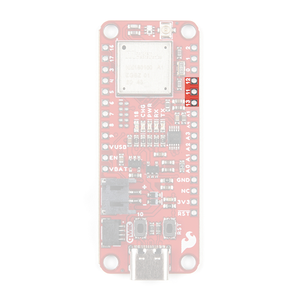
The SPI pins on the SparkFun expLoRaBLE. (Click to enlarge)
Note: To learn more about the serial peripheral interface (SPI) protocol, check out this great tutorial.
Serial Peripheral Interface (SPI)
I2C Communication Pins
The SparkFun expLoRaBLE has 2 I2C modules. The Qwiic connector is connected to the default I2C bus that is accessed through the Arduino IDE using the Wire module.
Buttons
There are two buttons on SparkFun expLoRaBLE; a reset and GPIO button.
Reset Button
The reset (RST) button allows users to reset the program running on the NM180100 SiP without unplugging the board.
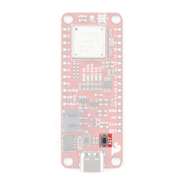
User Button
Note: In order to utilize the user button, connected to GPIO 10, the pin mode will need to be configured as an input with an internal pullup (i.e. INPUT_PULLUP); see an example below.
pinMode(D10, INPUT_PULLUP);
The user (10 ) button allows users to short GPIO 10 to ground (GND).

GPIO 10 button on the SparkFun expLoRaBLE. (Click to enlarge) Indicator LEDs
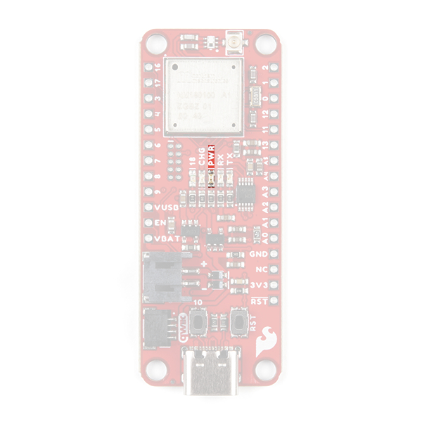
There are five indication LEDs on the SparkFun expLoRaBLE:
- Status/Pin 18 (Blue)
- Power (Red)
- Battery Charging (Yellow)
- RX (Yellow) and TX (Green)
Power LED
The red, PWR LED will light up once 3.3V is supplied to the board. For most users, it will light up when 5V is supplied through the USB connection and/or when a LiPo battery is attached to the JST connector.
PWR status LED indicator. (Click to enlarge) Battery Charging LED
The yellow, CHG LED will light while a battery is being charged through the charging circuit. The LED will be off when no battery is present (*dimmed), when the charge management controller is in standby (after the battery charging has been completed), or when the charge management controller is shutdown. The LED will be on when the charge management controller is in the process of charging the battery. For more information, please refer to the MCP73831 datasheet.

The battery charging (
CHG) LED indicator on the SparkFun expLoRaBLE Thing Plus. (Click to enlarge)
| Charge Cycle State | STAT1 |
|---|---|
Shutdown
|
Off (High Z) |
| No Battery Present | Dimmed (High Z) |
| Charge Complete – Standby | Off (H) |
| Preconditioning | On (L) |
| Constant-Current Fast Charge | On (L) |
| Constant Voltage | On (L) |
STAT LED
The blue, status (18) LED is typically used as a test or status LED to make sure that a board is working or for basic debugging. This indicator is connected to GPIO 18.
18) LED indicator on the SparkFun expLoRaBLE Thing Plus. (Click to enlarge) RX and TX LEDs
The yellow, RX and green, TX LEDs are used to indicate serial communication and programming between the CH340E serial-to-UART and NM180100 SiP.
RX and TX LED indicators on the SparkFun expLoRaBLE Thing Plus. (Click to enlarge) Jumpers
There are three jumpers on the back of the board that can be used to easily modify the hardware connections on the board.
- ISO - This jumper can be used to isolate the 3.3V connection from the voltage regulator.
- LED - This jumper can be used to remove 3.3V power to the
PWRLED and reduce power consumption on the board. - RTS - This jumper can be used to disconnect the CH340E from the
RESETpin of the Apollo3; effectively, disabling the ability of the CH340E to reset the MCU through software.
Primary I2C Bus
The Qwiic connector is attached to the primary I2C bus. The primary I2C bus for this board utilizes the pin connections, detailed in the table below:
| Connection | VDD |
GND |
SCL |
SDA |
|---|---|---|---|---|
|
Pad Number
(NM180100 SiP) |
3.3V | GND | D15 |
D14 |
Qwiic Connector
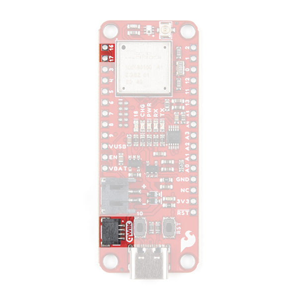
A Qwiic connector is provided for users to seamlessly integrate with SparkFun's Qwiic Ecosystem.
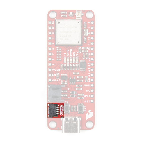
What is Qwiic?
The Qwiic system is intended a quick, hassle-free cabling/connector system for I2C devices. Qwiic is actually a play on words between "quick" and I2C or "iic".
Features of the Qwiic System
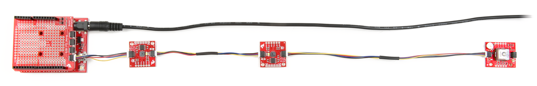
Keep your soldering iron at bay.
Cables plug easily between boards making quick work of setting up a new prototype. We currently offer three different lengths of Qwiic cables as well as a breadboard friendly cable to connect any Qwiic enabled board to anything else. Initially you may need to solder headers onto the shield to connect your platform to the Qwiic system but once that’s done it’s plug and go!
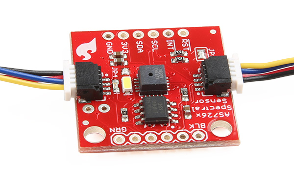
Qwiic cables connected to Spectral Sensor Breakout
Minimize your mistakes.
How many times have you swapped the SDA and SCL wires on your breadboard hoping the sensor will start working? The Qwiic connector is polarized so you know you’ll have it wired correctly, every time, from the start.
The PCB connector is part number SM04B-SRSS (Datasheet) or equivalent. The mating connector used on cables is part number SHR04V-S-B or equivalent. This is a common and low cost connector.
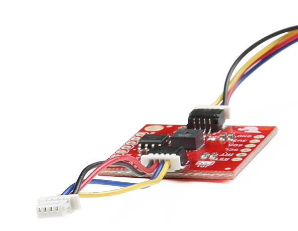
1mm pitch, 4-pin JST connector
Expand with ease.
It’s time to leverage the power of the I2C bus! Most Qwiic boards will have two or more connectors on them allowing multiple devices to be connected.