Si4707 Hookup Guide
 jimblom
Board and IC Overview
In the words of Silicon Labs, the Si4707 is "the industry's first weather band (WB) radio receiver to include a specific area message encoding (SAME) processor." It's a really neat chip. Aside from being able to tune to all weather band frequencies and process SAME messages, the Si4707 also hosts a variety of cool features. It's versatile: it can be interfaced with using either I2C, SPI, or a 3-wire interface. And, it's got a really clean-sounding audio quality.
Silicon Labs has produced a wealth of supporting material for the chip. All of it hosted on their website. Some of the really useful documents include:
- Si4707-B20 - The datasheet.
- AN332 - The Si4707 programming guide, where you'll find information about all of the Si4707's registers and settings.
It's important to point out that the Si4707 has a maximum interface supply voltage of 3.6V. When we connect it to an Arduino, it'll be powered by the 3.3V line. Voltage on the input lines should also be limited to about 3.3V as well.
Breakout Board Schematic
The Si4707 Breakout Board surrounds the Si4707 with all of the supporting circuitry one might need to hit the ground running with the chip.
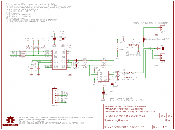
One of the more important parts surrounding the Si4707 is the 32.768kHz crystal, which provides the IC's reference clock. All of the I/O lines are pulled up to 3.3V through 4.7kΩ resistors. The antenna portion of the circuit has a filtering 56nH inductor and an ESD protecting diode.
The left and right analog audio outputs of the Si4707 are sent through a headphone amplifier (a TPA6111A2), which boosts the signal. The output of the amplifier is sent to a 3.5mm audio jack.
Board Pin-Out
The Si4707 Breakout has one main interface header and two smaller optional headers on the side of the board.
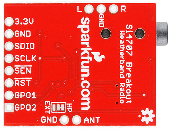
On the main header are the following pins:
- 3.3V - The supply voltage input. This will go to both the VDD and VIO pins of the Si4707. The supply voltage should be between 1.5 and 3.6V.
- GND - This supplies both the digital ground and RF ground of the Si4707.
- SDIO - Serial data input/output for all interfaces.
- SCLK - Serial clock input for all interfaces.
- SEN - Serial enable input. If used in I2C mode, this pin selects the 7-bit address of the IC. In SPI mode, this is the chip-select input.
- RST - The reset input. It's active-low, so connecting this pin to ground will turn the chip off.
- GPO1 - General purpose output 1.
- GPO2 - General purpose output 2. This pin also serves as an interrupt output if so configured.
Other pins not on the main 8-pin header are:
- ANT - This is connected to the FMI input of the Si4707--the WB RF input. If you'd like to use an external antenna, select this output pin on the jumper (on the bottom of the board, near the pin).
- L and R - These are the analog audio outputs from the headphone amplifier. If you'd rather not use the 3.5mm audio jack, you can use these headers instead.
Well, that explains the board. Now we can move on to hooking it up!