Qwiic 6DoF (LSM6DSO) Breakout Hookup Guide
 bboyho,
  Elias The Sparkiest,
  MTaylor
Hardware Overview
In this section, we'll highlight the features of the board. We recommend looking at the datasheet and application notes linked in the Resources and Going Further for more information on the LSM6DSO. Open them in a non-browser viewer that can display the index/table of contents in a pane. There is so much information, paned viewing is a must!
Power and Logic Levels
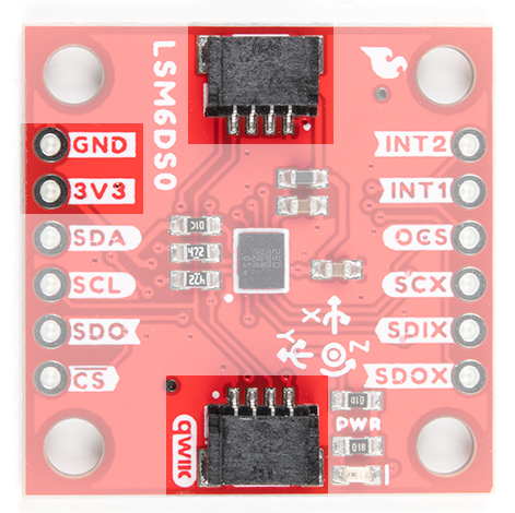
We recommend powering the board through the Qwiic connector when quickly prototyping. For a more secure connection, you can always solder to the PTH labeled 3V3 and GND. The recommended input voltage when using the board with a microcontroller is 3.3V if you are using the Qwiic connector. However, you can use a regulated supply voltage between 1.71V and 3.6V to power the sensor. The logic levels will match the input voltage (e.g. if the sensor is powered at 3.3V, the logic level will be 3.3V as well).
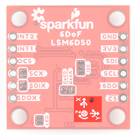
I2C
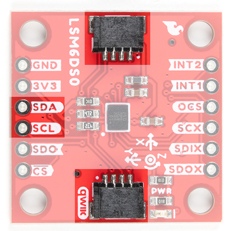
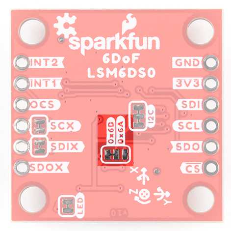
The main method of reading the LSM6DSO is through the I2C bus. The board includes two Qwiic connectors for fast prototyping and removes the need for soldering. All you need to do is plug a Qwiic cable into the Qwiic connector and voila! You can also solder to the PTHs labeled as SDA and SCL as an alternative. The default address for the IC is 0x6B. However, you can adjust the jumper on the back of the board to change the address to 0x6A.
SPI
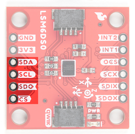
If you decide to use a SPI bus, you will need to solder header pins or wires to the board.
- SDA/SDI - Device data in. Note that the SDA pin used for I2C is also the SDI pin used for SPI. Flipping the board to the bottom side will show the label for the SPI pin.
- SCL - Serial clock for either I2C or SPI.
- SDO - Device data out. By default, the SDO pin is connected to power to set the I2C address. Make sure to cut the trace as explained below if you decide to use this sensor in SPI mode.
- CS - Chip select.
 |
 |
| Top of Board for SPI | Bottom of Board for SPI |
When using the board in SPI mode, you will need to cut the I2C jumper for the default address (e.g. 0x6B) on the back and leave the jumper pads unconnected when using SPI.
Interrupt Pins
INT1 and INT2 are programmable interrupts for the accelerometer and gyroscope. They can be set to alert on over/under thresholds, data ready, or FIFO overruns. Make sure these are connected to an INPUT pin to prevent driving 5v back into the LSM6DSO.
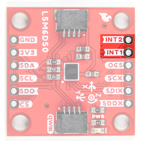
There are a variety of interrupts on the LSM6DSO. While connecting these is not as critical as the communication or power supply pins, using them will help you get the most out of the chip.
The interrupt pins are INT1 and INT2. One or both pins can be software configured and mapped to the following conditions:
- Step detected
- Step detected after delta time
- Step counter overflowed
- Significant motion (shock, drop)
- FIFO full
- FIFO overrun
- FIFO threshold reached (Datasheet calls this the "watermark")
- Boot status
- Gyroscope data ready
- Accelerometer data ready
- Inactivity
- Single tap
- Wake-up
- Free-fall
- Double tap
- 6D (orientation)
- Tilt
- Timer
- Ironing interrupt
Only a few interrupt examples are provided. See the datasheet and application guide for using the advanced interrupt features.
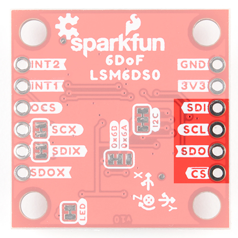
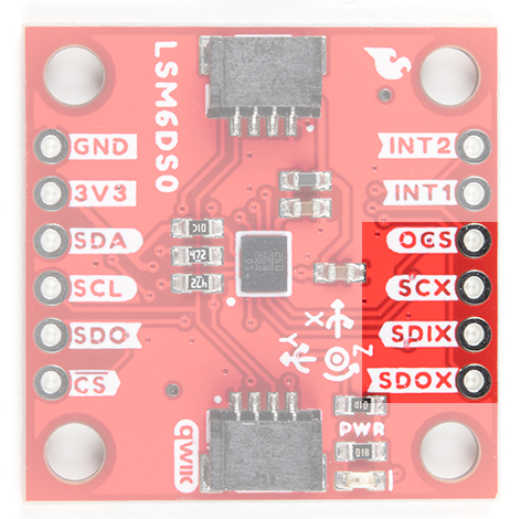
Auxiliary Pins
The auxiliary serial data output pins are used to attach slave I2C and auxiliary SPI 3/4-wire devices for FIFO data collection. This function is not covered in this tutorial.
- OCS - aux chip select
- SCX - aux serial clock
- SDIX - aux serial data input
- SDOX - aux serial data output
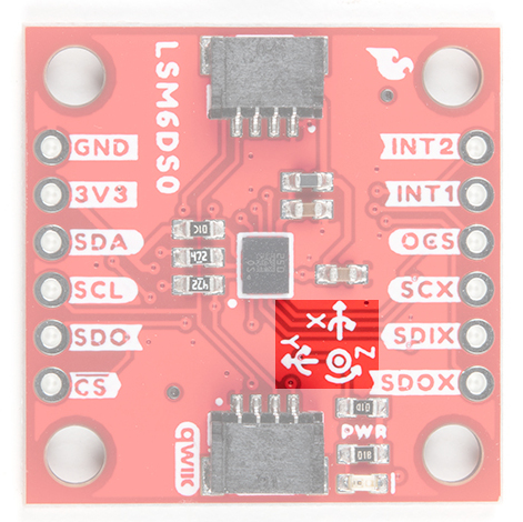
Reference Axis
For easy reference, we've documented the 6DoF's vectors with 3D Cartesian coordinate axes on the top and bottom side of the board. Make sure to orient and mount the board correctly for your application. Remember, it's all relative.
 |
 |
| 6DoF Reference (Top) | 6DoF Reference (Bottom) |
LED
The board includes an LED indicator that lights up when there is power available.
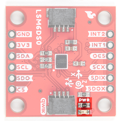
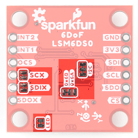
Jumper Pins
There are five jumpers on the back of the board. For more information, check out our tutorial on working with jumper pads and PCB traces should you decide to cut the traces with a hobby knife.
- LED - This is connected to the PWR LED on the top of the board. Cutting this disables the LED.
- I2C - The I2C jumper is connected to the 4.7kΩ pull-up resistors for the I2C bus. Most of the time you can leave these alone unless your project requires you to disconnect the pull-up resistors. SPI works with these connected but really should be cut apart for better signal shape at high speeds and to lower power consumption.
- 0x6B/0x6A - These jumpers are used to select the address 0x6B (default) or 0x6A for I2C communication. This jumper must be opened for SPI mode or the SDO line will not supply data.
- SCX - By default, this pin is connected to GND since ST recommends pulling the unused SCX to power or ground when not in use. For most users, you can leave this jumper alone. If your project requires connecting slave devices to the auxiliary pin, cut this trace.
- SDIX - By default, this pin is connected to GND since ST recommends pulling the unused SDIX to power or ground when not in use. For most users, you can leave this jumper alone. If your project requires connecting slave devices to the auxiliary pin, cut this trace.
Board Dimensions
The board uses the standard Qwiic size 1.0"x1.0" with four mounting holes by each corner.
