MicroMod Single Pair Ethernet Function Board - ADIN1110 Hookup Guide
 QCPete,
  El Duderino
Hardware Overview
In this section we'll take a closer look at the hardware on this Function Board along with a brief overview of what exactly 10BASE-T1L Single Pair Ethernet is and what benefits it provides.
10BASE-T1L Single Pair Ethernet
The 10BASE-T1L Single Pair Ethernet (SPE) standard uses just a single twisted pair for data as well as power. 10BASE-T1L Ethernet transmits data at speeds up to 10Mbps at distances up to 1.7km. With just a single pair, the cable is smaller and lighter making it ideal for remote monitoring or industrial applications connecting a large number of edge devices to a network connection.
For more information about 10BASE-T1L SPE, refer to this article on the communication protocol from Analog Devices or this SparkFun news post.
ADIN1110
The ADIN1110 is an ultra-low power Ethernet transceiver for 10BASE-T1L IEEE Standard 802.3cg-2019 SPE.
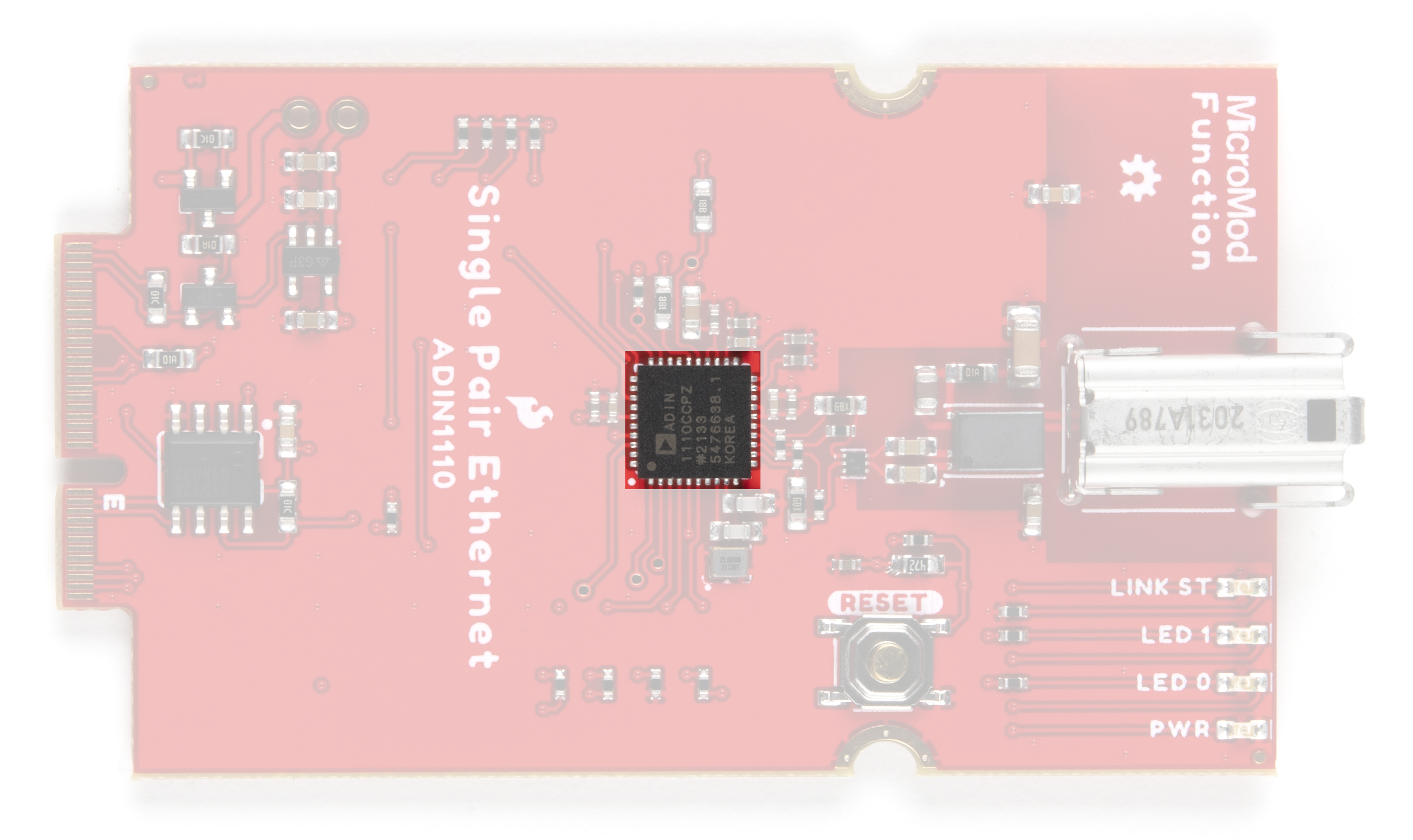
It operates from a supply voltage of 1.8V or 3.3V. This Function Board runs the ADIN1110 in single-supply mode at 3.3V (VDD_H and VVD_L are both powered at 3.3V) and this allows for transmission amplitude of 2.4V. For a complete overview of the ADIN1110 IC, refer to the datasheet.
The ADIN1110 MAC supports 16 individual MAC addresses and communicates over both Open Alliance and generic SPI protocols. The ADIN1110 transmits data at half duplex when using generic SPI and full duplex when using the Open Alliance protocol. The IC also includes support for three LED outputs, a Link LED and two configurable general purpose LEDs. The Function Board breaks out all of those to LEDs on board. Read on to the LEDs section below for more information.
SPE Data Output
The Function Board routes the ADIN1110's data signal pairs through a TVS diode protection circuit and phase transformer from Würth Elektronik before terminating in a specialized T1 Industrial Jack for connection to a separate SPE device or network hub.
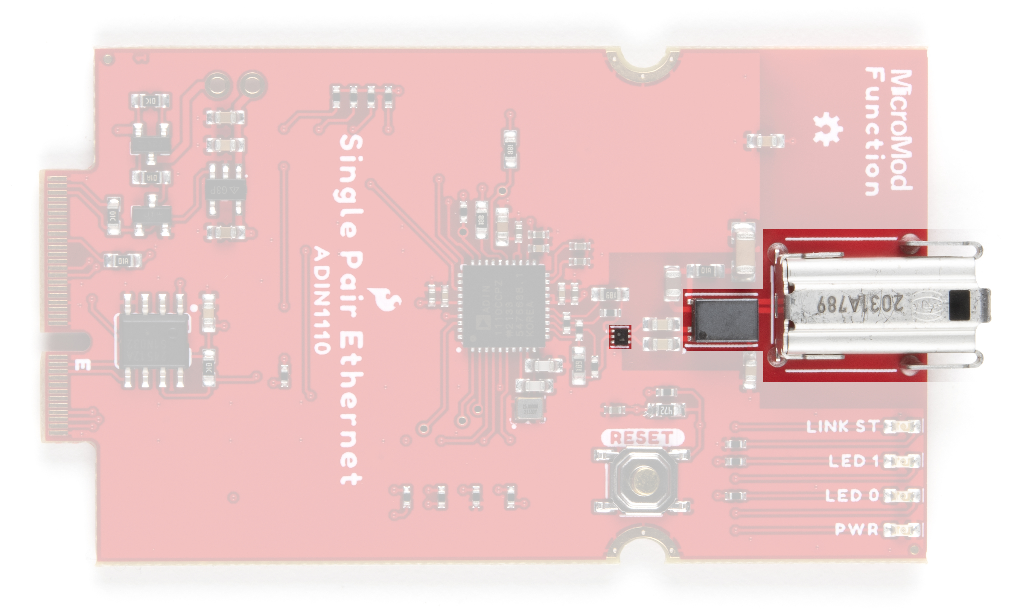
For more information about the TZ Industrial Jack, refer to the datasheet.
Power
The Function Board receives power from the Main Board it connects to. The Main Board can be powered either via USB or a connected LiPo battery. Reminder, this Function Board is not designed to send power over the Single Pair Ethernet connection.
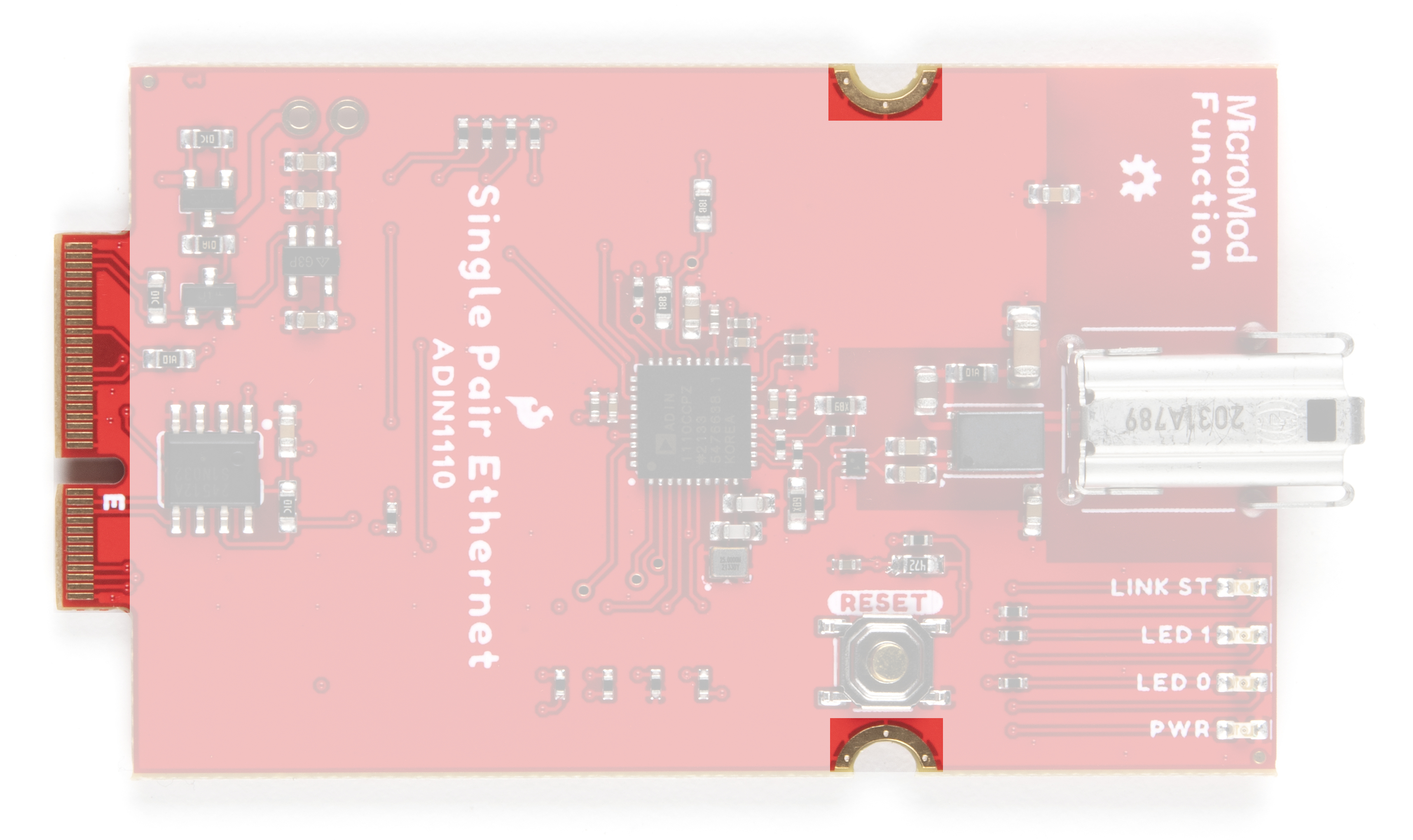
LEDs
This Function Board includes four LEDs labeled PWR, LED 0, LED 1 and LINK ST.
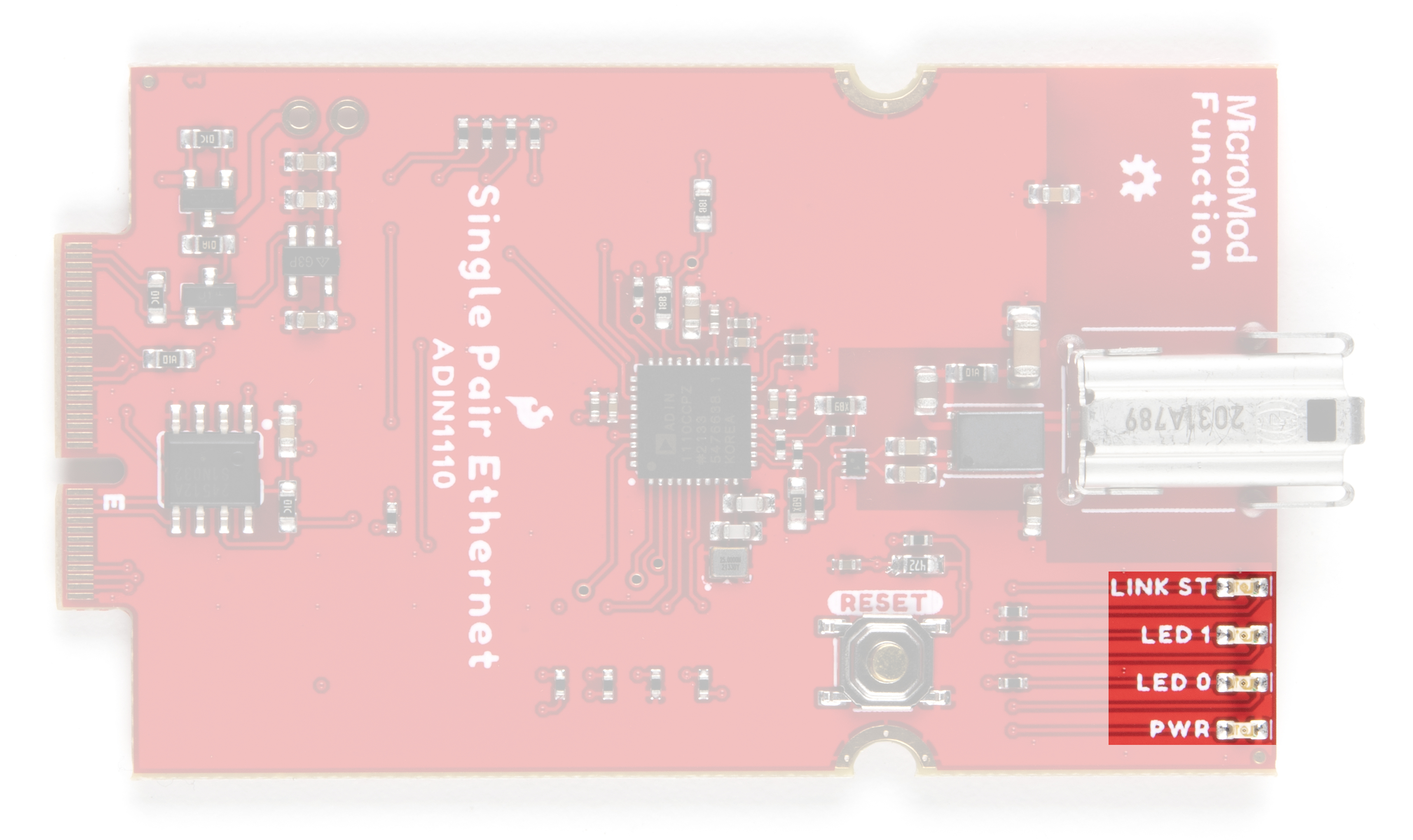
- PWR - Power LED.
- LED 0 - General purpose programmable LED. Active LOW. Default configuration turns the LED on when a link is established and blinks on activity.
- LED 1 - General purpose programmable LED. Active LOW. Default configuration disables the LED.
- LINK ST - Link status LED. Active HIGH. LED illuminates with a valid link.
For detailed instructions on programming the general purpose LEDs, refer to the LED Control Register section of the ADIN1110 Datasheet or the SparkFun ADIN1110 Arduino Library.
Solder Jumpers
This function board has twelve solder jumpers. The table below outlines each jumper's label, function, default states and any notes about their use.

| Label | Default State | Function | Notes |
|---|---|---|---|
| SHLD | CAP (See note) | Double jumper to select connector shield grounding option. | Default connects the connector shield to ground through a 3.3nF capacitor. Switch to GND side to connect the shield directly to ground. |
| LED1 | CLOSED | Completes LED1 configurable LED circuit. | Open to disable the labeled LED. Helps reduce the total current draw. |
| LINKST | CLOSED | Completes the Link Status LED circuit. | |
| LED0 | CLOSED | Completes the LED0 configurable LED circuit. | |
| PWR | CLOSED | Completes the Power LED circuit. | |
| TX2P4 EN | OPEN | Pulls TX2P4_EN pin LOW. | Controls the transmit amplitude mode. By default, this pin is LOW and allows both 1.0V and 2.4V p-p transmit levels. Pulling this pin high disables 2.4V transmit level.1 |
| SWPD EN | OPEN | Pulls SWPD_EN pin LOW. | Controls whether or not the ADIN1110 enters software power-down mode after reset. By default, the ADIN1110 starts autonegotiation after a reset. If the jumper is closed, the ADIN1110 remains in power-down mode after reset until it is configured over SPI. This allows software control over power-down mode.1 |
| MS SEL | OPEN | Sets the ADIN1110 to operate as a peripheral (slave) device on SPI. | Controls whether the ADIN1110 defaults to a controller or peripheral on the SPI bus.1 |
| SPI CFG1 | OPEN | Sets the ADIN1110 to use OPEN Aliance SPI protocol with protection (if SPI_CFG0 is also LOW). | |
| SPI CFG0 | OPEN | Sets the ADIN1110 to use OPEN Aliance SPI protocol with protection (if SPI_CFG1 is also LOW). | |
| EWP | OPEN | EEPROM write protection. | |
| MEAS | CLOSED | Ties VCC_IN to input on 3.3V voltage regulator. | Open to measure current draw of the board. |
MicroMod Edge Connector and Pinout
The MicroMod ecosystem uses a polarized M.2 edge connector to provide a standardized electrical connection that is keyed to prevent incorrect connection between MicroMod boards. The attachment points for the screws prevent users from connecting a processor board into a function board slot and vice-versa.
MicroMod Pinout
This Function Board uses the following pins on a connected Processor Board:
- 3.3V & VCC
- Power enable
- SPI - ADIN1110 Communication
- I2C - EEPROM Comunication
- D0 (Slot 0) / D1 (Slot 1) - ADIN1110 Interrupt
- CS0 (Slot 0) / CS1 (Slot 1) - ADIN1110 Chip Select (SPI)
For the complete MicroMod Pinout and pins used by this function board, take a look at the tables below:
| AUDIO | UART | GPIO/BUS | I2C | SDIO | SPI0 | Dedicated |
| Function | Bottom Pin |
Top Pin |
Function | ||||||
|---|---|---|---|---|---|---|---|---|---|
| (Not Connected) | 75 | GND | |||||||
| 3.3V | 74 | 73 | G5 / BUS5 | ||||||
| RTC_3V_BATT | 72 | 71 | G6 / BUS6 | ||||||
| SPI_CS1# | SDIO_DATA3 (I/O) | 70 | 69 | G7 / BUS7 | |||||
| SDIO_DATA2 (I/O) | 68 | 67 | G8 | ||||||
| SDIO_DATA1 (I/O) | 66 | 65 | G9 | ADC_D- | CAM_HSYNC | ||||
| SPI_CIPO1 | SDIO_DATA0 (I/O) | 64 | 63 | G10 | ADC_D+ | CAM_VSYNC | |||
| SPI COPI1 | SDIO_CMD (I/O) | 62 | 61 | SPI_CIPO (I) | |||||
| SPI SCK1 | SDIO_SCK (O) | 60 | 59 | SPI_COPI (O) | LED_DAT | ||||
| AUD_MCLK (O) | 58 | 57 | SPI_SCK (O) | LED_CLK | |||||
| CAM_MCLK | PCM_OUT | I2S_OUT | AUD_OUT | 56 | 55 | SPI_CS# | |||
| CAM_PCLK | PCM_IN | I2S_IN | AUD_IN | 54 | 53 | I2C_SCL1 (I/O) | |||
| PDM_DATA | PCM_SYNC | I2S_WS | AUD_LRCLK | 52 | 51 | I2C_SDA1 (I/O) | |||
| PDM_CLK | PCM_CLK | I2S_SCK | AUD_BCLK | 50 | 49 | BATT_VIN / 3 (I - ADC) (0 to 3.3V) | |||
| G4 / BUS4 | 48 | 47 | PWM1 | ||||||
| G3 / BUS3 | 46 | 45 | GND | ||||||
| G2 / BUS2 | 44 | 43 | CAN_TX | ||||||
| G1 / BUS1 | 42 | 41 | CAN_RX | ||||||
| G0 / BUS0 | 40 | 39 | GND | ||||||
| A1 | 38 | 37 | USBHOST_D- | ||||||
| GND | 36 | 35 | USBHOST_D+ | ||||||
| A0 | 34 | 33 | GND | ||||||
| PWM0 | 32 | 31 | Module Key | ||||||
| Module Key | 30 | 29 | Module Key | ||||||
| Module Key | 28 | 27 | Module Key | ||||||
| Module Key | 26 | 25 | Module Key | ||||||
| Module Key | 24 | 23 | SWDIO | ||||||
| UART_TX2 (O) | 22 | 21 | SWDCK | ||||||
| UART_RX2 (I) | 20 | 19 | UART_RX1 (I) | ||||||
| CAM_TRIG | D1 | 18 | 17 | UART_TX1 (0) | |||||
| I2C_INT# | 16 | 15 | UART_CTS1 (I) | ||||||
| I2C_SCL (I/0) | 14 | 13 | UART_RTS1 (O) | ||||||
| I2C_SDA (I/0) | 12 | 11 | BOOT (I - Open Drain) | ||||||
| D0 | 10 | 9 | USB_VIN | ||||||
| SWO | G11 | 8 | 7 | GND | |||||
| RESET# (I - Open Drain) | 6 | 5 | USB_D- | ||||||
| 3.3V_EN | 4 | 3 | USB_D+ | ||||||
| 3.3V | 2 | 1 | GND | ||||||
| Description | Function | Bottom Pin |
Top Pin |
Function | Description |
|---|---|---|---|---|---|
| (Not Connected) | 75 | GND | |||
| - | 74 | 73 | 3.3V | Power Supply: 3.3-6V | |
| - | 72 | 71 | Power EN | Power Enable | |
| - | 70 | 69 | - | ||
| - | 66 | 65 | - | ||
| - | 64 | 63 | - | ||
| - | 62 | 61 | - | ||
| - | 60 | 59 | - | ||
| - | 58 | 57 | - | ||
| - | 56 | 55 | RESET | ADIN1110 Reset Button | |
| - | 54 | 53 | - | ||
| - | 52 | 51 | - | ||
| - | 50 | 49 | CS | ADIN1110 Chip Select | |
| - | 48 | 47 | INT | ADIN1110 Interrupt Pin | |
| - | 46 | 45 | GND | ||
| - | 44 | 43 | - | ||
| - | 42 | 41 | - | ||
| Write protection pin for the EEPROM. Pull low to enable. | EEPROM_WP | 40 | 39 | GND | |
| - | 38 | 37 | - | ||
| EEPROM I2C address configuration. | EEPROM_A0 | 36 | 35 | - | |
| EEPROM I2C address configuration. | EEPROM_A1 | 34 | 33 | GND | |
| EEPROM I2C address configuration. | EEPROM_A2 | 32 | 31 | Module Key | |
| Module Key | 30 | 29 | Module Key | ||
| Module Key | 28 | 27 | Module Key | ||
| Module Key | 26 | 25 | Module Key | ||
| Module Key | 24 | 23 | - | ||
| - | 22 | 21 | I2C_SCL | I2C - Clock signal for EEPROM | |
| - | 20 | 19 | I2C_SDA | I2C - Data signal for EEPROM | |
| - | 18 | 17 | - | ||
| - | 16 | 15 | - | ||
| - | 14 | 13 | - | ||
| - | 12 | 11 | - | ||
| - | 10 | 9 | - | ||
| - | 8 | 7 | POCI | SPI Peripheral Output/Controller Input. | |
| - | 6 | 5 | PICO | SPI Peripheral Input/Controller Output. | |
| - | 4 | 3 | SCK | SPI Clock Signal | |
| - | 2 | 1 | GND |
| Signal Group | Signal | I/O | Description | Voltage | Power | 3.3V | I | 3.3V Source | 3.3V |
|---|---|---|---|---|
| GND | Return current path | 0V | ||
| USB_VIN | I | USB VIN compliant to USB 2.0 specification. Connect to pins on processor board that require 5V for USB functionality | 4.8-5.2V | |
| RTC_3V_BATT | I | 3V provided by external coin cell or mini battery. Max draw=100μA. Connect to pins maintaining an RTC during power loss. Can be left NC. | 3V | |
| 3.3V_EN | O | Controls the carrier board's main voltage regulator. Voltage above 1V will enable 3.3V power path. | 3.3V | |
| BATT_VIN/3 | I | Carrier board raw voltage over 3. 1/3 resistor divider is implemented on carrier board. Amplify the analog signal as needed for full 0-3.3V range | 3.3V | |
| Reset | Reset | I | Input to processor. Open drain with pullup on processor board. Pulling low resets processor. | 3.3V |
| Boot | I | Input to processor. Open drain with pullup on processor board. Pulling low puts processor into special boot mode. Can be left NC. | 3.3V | |
| USB | USB_D± | I/O | USB Data ±. Differential serial data interface compliant to USB 2.0 specification. If UART is required for programming, USB± must be routed to a USB-to-serial conversion IC on the processor board. | |
| USB Host | USBHOST_D± | I/O | For processors that support USB Host Mode. USB Data±. Differential serial data interface compliant to USB 2.0 specification. Can be left NC. | |
| CAN | CAN_RX | I | CAN Bus receive data. | 3.3V |
| CAN_TX | O | CAN Bus transmit data. | 3.3V | |
| UART | UART_RX1 | I | UART receive data. | 3.3V |
| UART_TX1 | O | UART transmit data. | 3.3V | |
| UART_RTS1 | O | UART ready to send. | 3.3V | |
| UART_CTS1 | I | UART clear to send. | 3.3V | |
| UART_RX2 | I | 2nd UART receive data. | 3.3V | |
| UART_TX2 | O | 2nd UART transmit data. | 3.3V | |
| I2C | I2C_SCL | I/O | I2C clock. Open drain with pullup on carrier board. | 3.3V |
| I2C_SDA | I/O | I2C data. Open drain with pullup on carrier board | 3.3V | |
| I2C_INT# | I | Interrupt notification from carrier board to processor. Open drain with pullup on carrier board. Active LOW | 3.3V | |
| I2C_SCL1 | I/O | 2nd I2C clock. Open drain with pullup on carrier board. | 3.3V | |
| I2C_SDA1 | I/O | 2nd I2C data. Open drain with pullup on carrier board. | 3.3V | |
| SPI | SPI_PICO | O | SPI Peripheral Input/Controller Output. | 3.3V |
| SPI_POCI | I | SPI Peripheral Output/Controller Input. | 3.3V | |
| SPI_SCK | O | SPI Clock. | 3.3V | |
| SPI_CS# | O | SPI Chip Select. Active LOW. Can be routed to GPIO if hardware CS is unused. | 3.3V | |
| SPI/SDIO | SPI_SCK1/SDIO_CLK | O | 2nd SPI Clock. Secondary use is SDIO Clock. | 3.3V |
| SPI_PICO1/SDIO_CMD | I/O | 2nd SPI Peripheral Input/Controller Output. Secondary use is SDIO command interface. | 3.3V | |
| SPI_POCI1/SDIO_DATA0 | I/O | 2nd SPI Controller Output/Peripheral Input. Secondary use is SDIO data exchange bit 0. | 3.3V | |
| SDIO_DATA1 | I/O | SDIO data exchange bit 1. | 3.3V | |
| SDIO_DATA2 | I/O | SDIO data exchange bit 2. | 3.3V | |
| SPI_CS1/SDIO_DATA3 | I/O | 2nd SPI Chip Select. Secondary use is SDIO data exchange bit 3. | 3.3V | |
| Audio | AUD_MCLK | O | Audio master clock. | 3.3V |
| AUD_OUT/PCM_OUT/I2S_OUT/CAM_MCLK | O | Audio data output. PCM synchronous data output. I2S serial data out. Camera master clock. | 3.3V | |
| AUD_IN/PCM_IN/I2S_IN/CAM_PCLK | I | Audio data input. PCM syncrhonous data input. I2S serial data in. Camera periphperal clock. | 3.3V | |
| AUD_LRCLK/PCM_SYNC/I2S_WS/PDM_DATA | I/O | Audio left/right clock. PCM syncrhonous data SYNC. I2S word select. PDM data. | 3.3V | |
| AUD_BCLK/PCM_CLK/I2S_CLK/PDM_CLK | O | Audio bit clock. PCM clock. I2S continuous serial clock. PDM clock. | 3.3V | |
| SWD | SWDIO | I/O | Serial Wire Debug I/O. Connect if processor board supports SWD. Can be left NC. | 3.3V |
| SWDCK | I | Serial Wire Debug clock. Connect if processor board supports SWD. Can be left NC. | 3.3V | |
| ADC | A0 | I | Analog to digital converter 0. Amplify the analog signal as needed to enable full 0-3.3V range. | 3.3V |
| A1 | I | Analog to digital converter 1. Amplify the analog signal as needed to enable full 0-3.3V range. | 3.3V | |
| PWM | PWM0 | O | Pulse width modulated output 0. | 3.3V |
| PWM1 | O | Pulse width modulated output 1. | 3.3V | |
| Digital | D0 | I/O | General digital input/output pin. | 3.3V |
| D1/CAM_TRIG | I/O | General digital input/output pin. Camera trigger. | 3.3V | |
| General/Bus | G0/BUS0 | I/O | General purpose pins. Any unused processor pins should be assigned to Gx with ADC + PWM capable pins given priority (0, 1, 2, etc.) positions. The intent is to guarantee PWM, ADC and Digital Pin functionality on respective ADC/PWM/Digital pins. Gx pins do not guarantee ADC/PWM function. Alternative use is pins can support a fast read/write 8-bit or 4-bit wide bus. | 3.3V |
| G1/BUS1 | I/O | 3.3V | ||
| G2/BUS2 | I/O | 3.3V | ||
| G3/BUS3 | I/O | 3.3V | ||
| G4/BUS4 | I/O | 3.3V | ||
| G5/BUS5 | I/O | 3.3V | ||
| G6/BUS6 | I/O | 3.3V | ||
| G7/BUS7 | I/O | 3.3V | ||
| G8 | I/O | General purpose pin | 3.3V | |
| G9/ADC_D-/CAM_HSYNC | I/O | Differential ADC input if available. Camera horizontal sync. | 3.3V | |
| G10/ADC_D+/CAM_VSYNC | I/O | Differential ADC input if available. Camera vertical sync. | 3.3V | |
| G11/SWO | I/O | General purpose pin. Serial Wire Output | 3.3V |
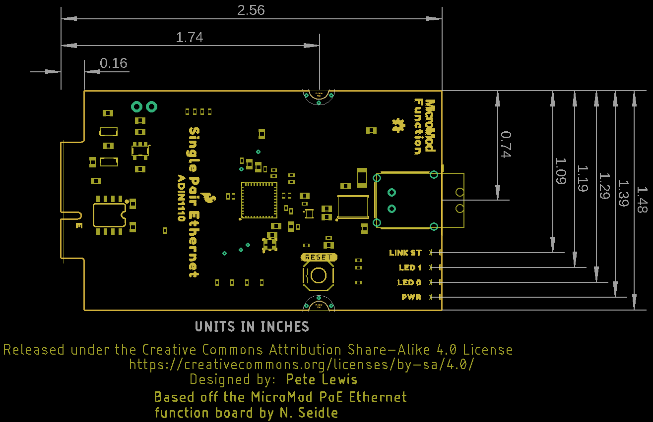
Board Dimensions
This Function Board uses the standard sizing for MicroMod Function Boards and measures 2.56" x 1.48" (65.02mm x 37.59mm) and the T1 jack protrudes roughly 0.15" (3.81mm) from the edge of the board.