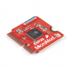
MicroMod GNSS Function Board - ZED-F9P Hookup Guide
 El Duderino
 Introduction
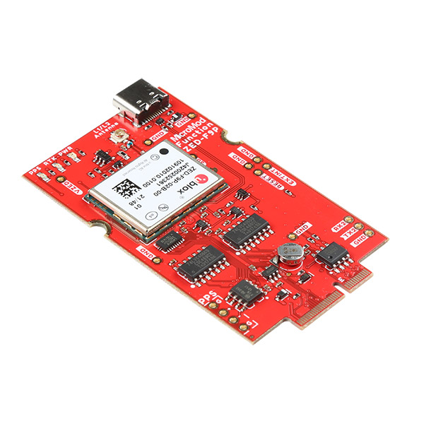
As some readers may guess by the assortment of SparkFun products featuring it, we love the ZED-F9P GNSS module from u-blox. The SparkFun MicroMod GNSS Function Board - ZED-F9P provides high precision GNSS capabilities for MicroMod projects using Main Board/Function Board assemblies. The ZED-F9P module from u-blox is capable of up to 10mm 3-dimensional accuracy though the module requires a clear view of the sky as well as correction data from an RTCM source to achieve this accuracy. The ZED-F9P can act as a base station as well so you can use it with a second Function Board (or another SparkFun ZED-F9P product) together to achieve millimeter positional accuracy.
Having the ZED-F9P on a MicroMod Function board allows for even more versatility with projects using the ZED-F9P allowing users to mix and match not only their preferred Processor but also to pair it with another Function Board to add even more versatility to a GNSS project.
This guide will go over the hardware present on this Function Board, how to assemble it into a MicroMod circuit as well as an Arduino example to start getting location data from the ZED-F9P.
Required Materials
You'll need the following materials along with the MicroMod GNSS Function Board - ZED-F9P to complete this tutorial and use the Function Board.
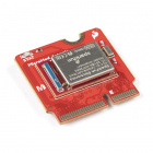
Main Board
All Function Boards require a Main Board and Processor to connect to each other. Depending on your application, you may need either a Single or Dual Main Board:
SparkFun MicroMod Main Board - Single
DEV-18575
SparkFun MicroMod Main Board - Double
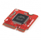
DEV-18576Processor Board
You'll need a Processor Board to act as a host controller for the Function Board:
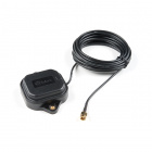
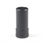
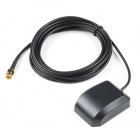
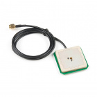
Antenna
The GNSS Function Board also requires an antenna. We recommend using a GNSS multi-band antenna compatible with both L1 and L2 bands for full reception like the ones below:
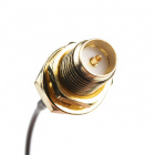
Antenna Accessories
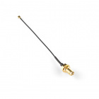
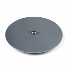
The GNNS Function Board uses a u.Fl connector for the antenna connection so in order to use the antennas listed above, you will need an adapter cable like the ones below. You may also want a grounding plate to maximize your antenna's reception:
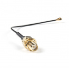
Interface Cable U.FL to SMA - 100mm
WRL-18154Suggested Reading
The MicroMod ecosystem is a unique way to allow users to customize their project to their needs. If you aren't familiar with the MicroMod system, click on the banner below for more information.
Before getting started, be sure to check out our What is GPS RTK? tutorial and if you're not familiary with u-center, have a look at our Getting Started with U-Center as well as these related tutorials:
I2C
Serial Basic Hookup Guide
What is GPS RTK?
Getting Started with U-Center for u-blox
This tutorial is based around the guide for the SparkFun GPS-RTK2 Board - ZED-F9P so you may want to check out these tutorials for more information on GPS-RTK:
GPS-RTK Hookup Guide
GPS-RTK2 Hookup Guide
Hardware Overview
Let's take a closer look at the ZED-F9P module and other hardware on this Function Board.
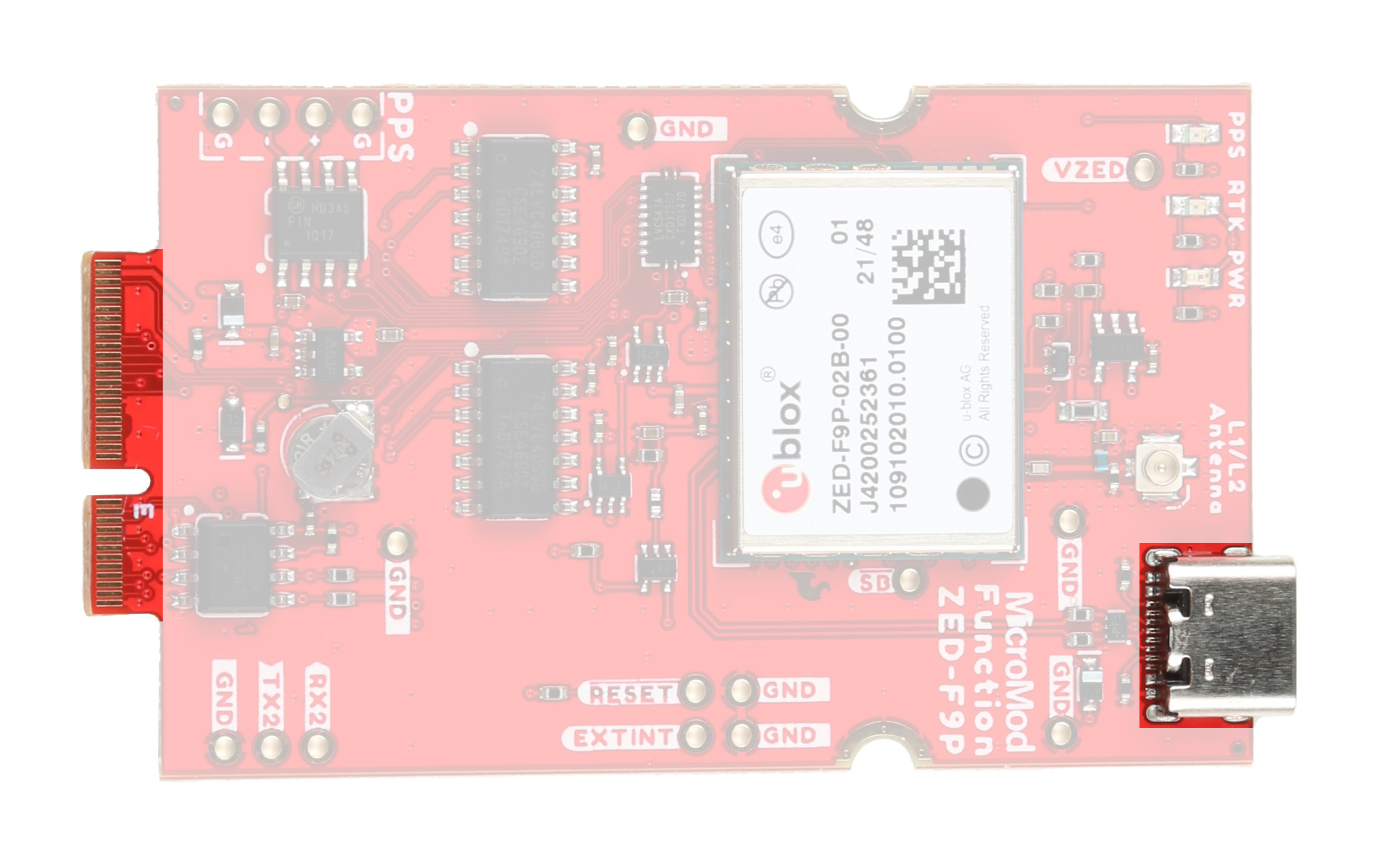
ZED-F9P GNSS Module
The ZED-F9P is a high-precision GNSS module from u-blox capable of up to millimeter X, Y & Z positional accuracy.
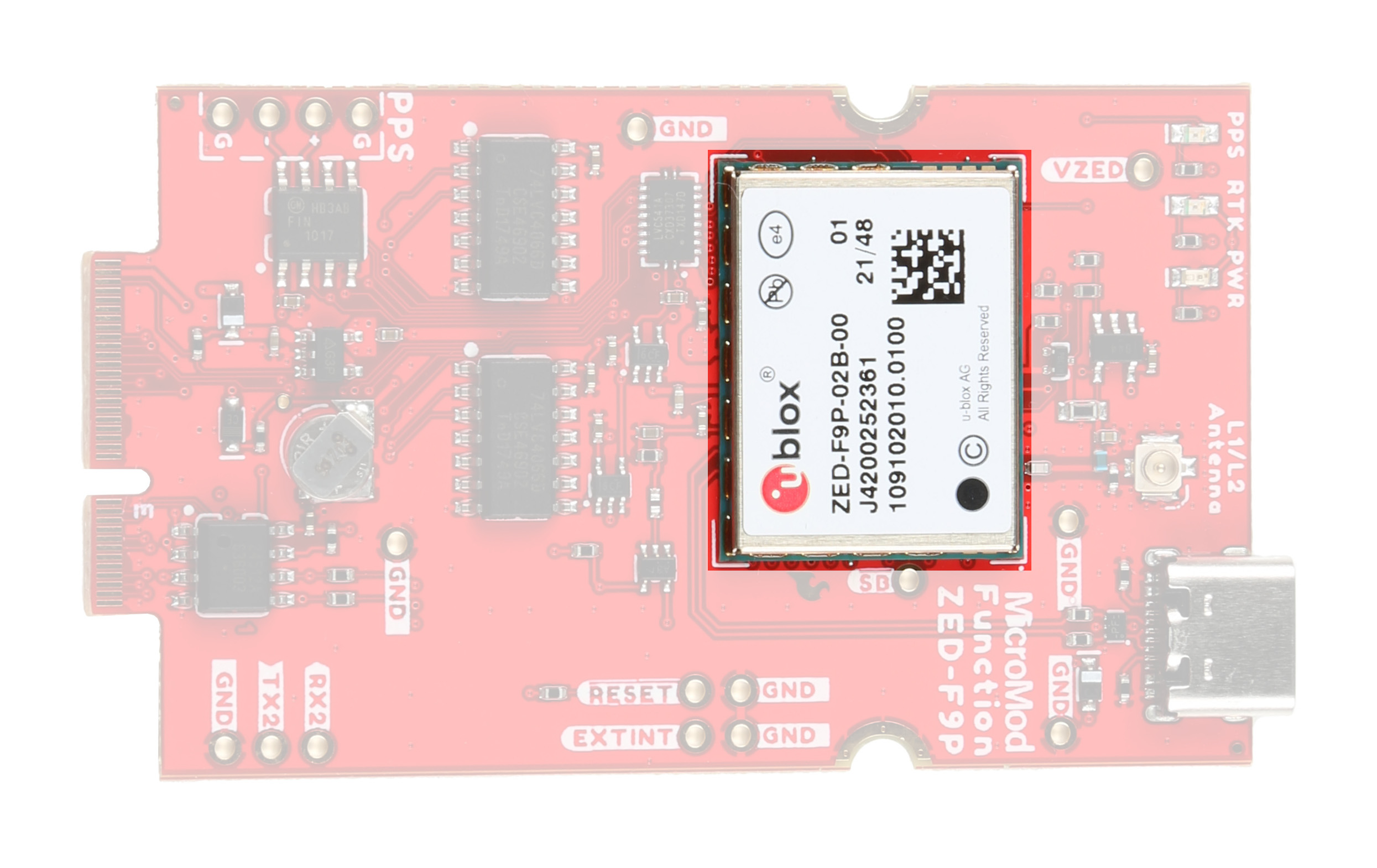
The ZED-F9P with a full RTK lock along with RTCM data streaming to the module can achieve 10mm 3D positional accuracy. Depending on the constellation the module achieves a lock in ~25 seconds from a cold start and 2 seconds from both a hot start and aided start. For a complete overview of the module, refer to the ZED-F9P datasheet.
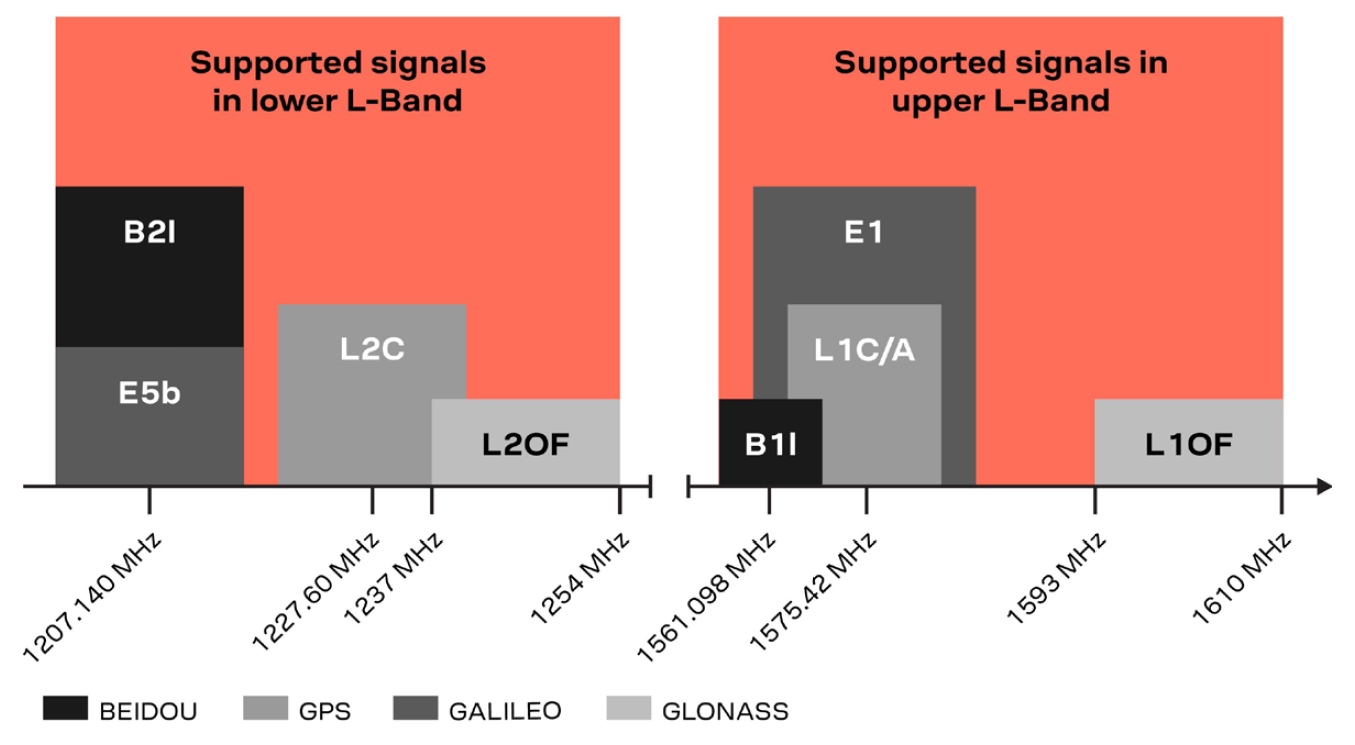
One of the key differentiators between the ZED-F9P and almost all other low-cost RTK solutions is the ZED-F9P is capable of receiving both L1 and L2 bands.
The module can act as either a rover to receive GNNS location data and RTCM correction data or a base station to send RTCM correction data to another device. For complete information on how to configure the ZED-F9P as a base station or rover, refer to the u-blox Integration Manual or check out this tutorial.
Communication Interfaces
This Function Board routes the ZED-F9P's USB interface to a USB-C connector on the top of the board. The SPI, I2C and primary serial interfaces are routed to the MicroMod M.2 connector through an isolation circuit.
The board configures the ZED-F9P to communicate via I2C and Serial by default. Adjusting the DSEL solder jumper switches the communication interface to SPI.
The USB-C connector allows direct communication to the ZED-F9P UART interface but does not provide power to the module or other parts of the MicroMod assembly by default. To use this connector for power, adjust the USB PWR EN jumper. Read on to the Solder Jumpers section for more information.
Antenna
The board routes the ZED-F9P antenna connection to a u.Fl connector for an external antenna connection. Most of the recommended antennas use a SMA-type connector so an adapter like this is most likely needed.
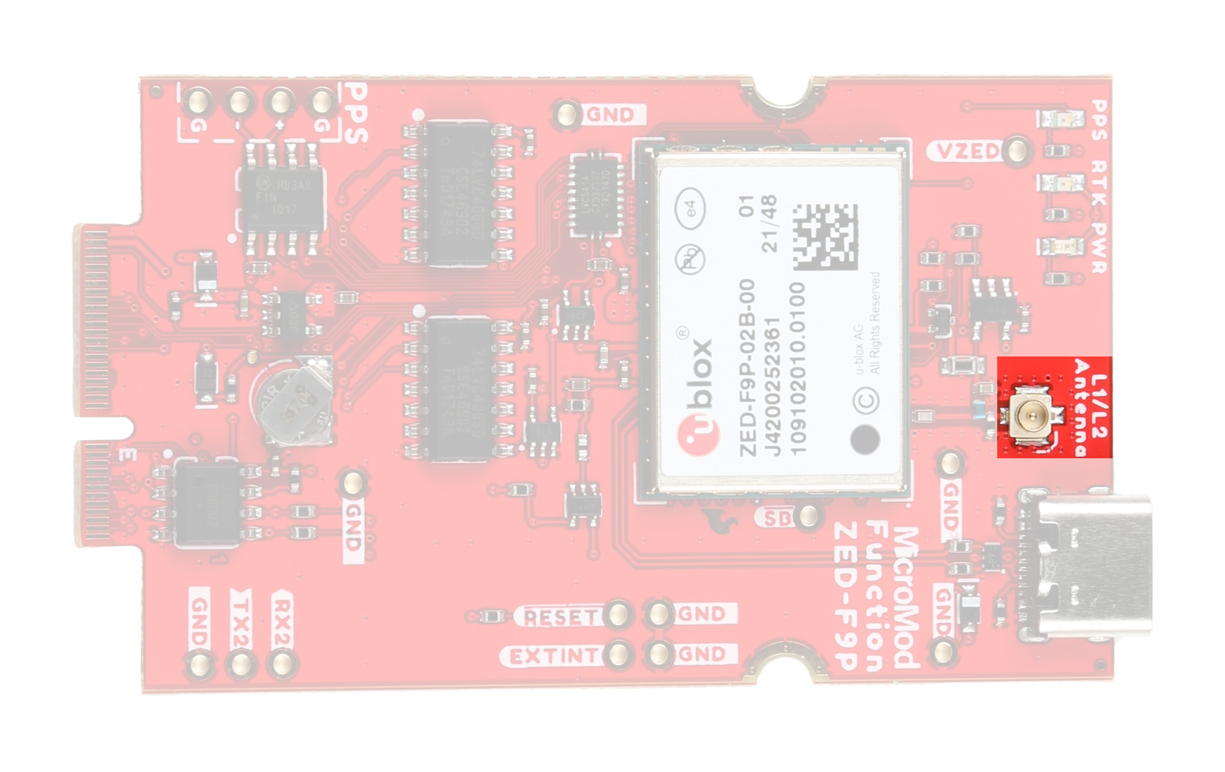
The Function Board also includes a RF/antenna supervision circuit to monitor and control the active antenna connection. The supervision circuit protects the ZED-F9P from a short circuit on the antenna connection and monitors the antenna connection to detect a connected antenna or open circuit. By default the Function Board disables this circuit through the SUP solder jumper. Read on to the Solder Jumpers section for more information on using this jumper and refer to section 4.3.4 of the ZED-F9P Integration Manual for more information on this circuit and how to poll the status using UBX messages.
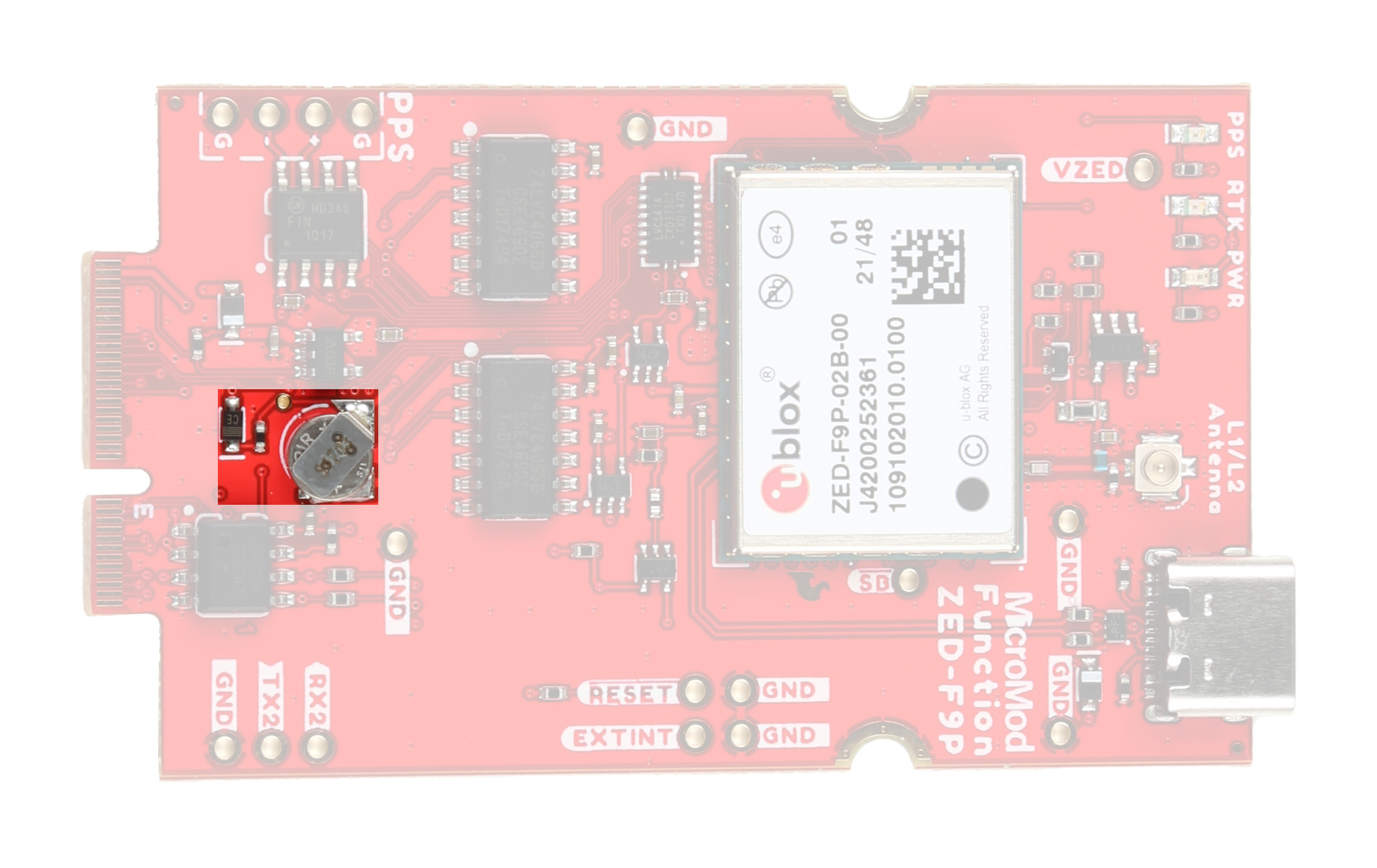
Backup Battery
The backup battery on the board has a 1.5mAh capacity to maintain settings and other low-power functionality to the ZED-F9P when the module is not fully powered.
PTH Connections
Along with the secondary serial bus, the Function Board routes several other ZED-F9P pins to plated through-hole (PTH) connecitons.
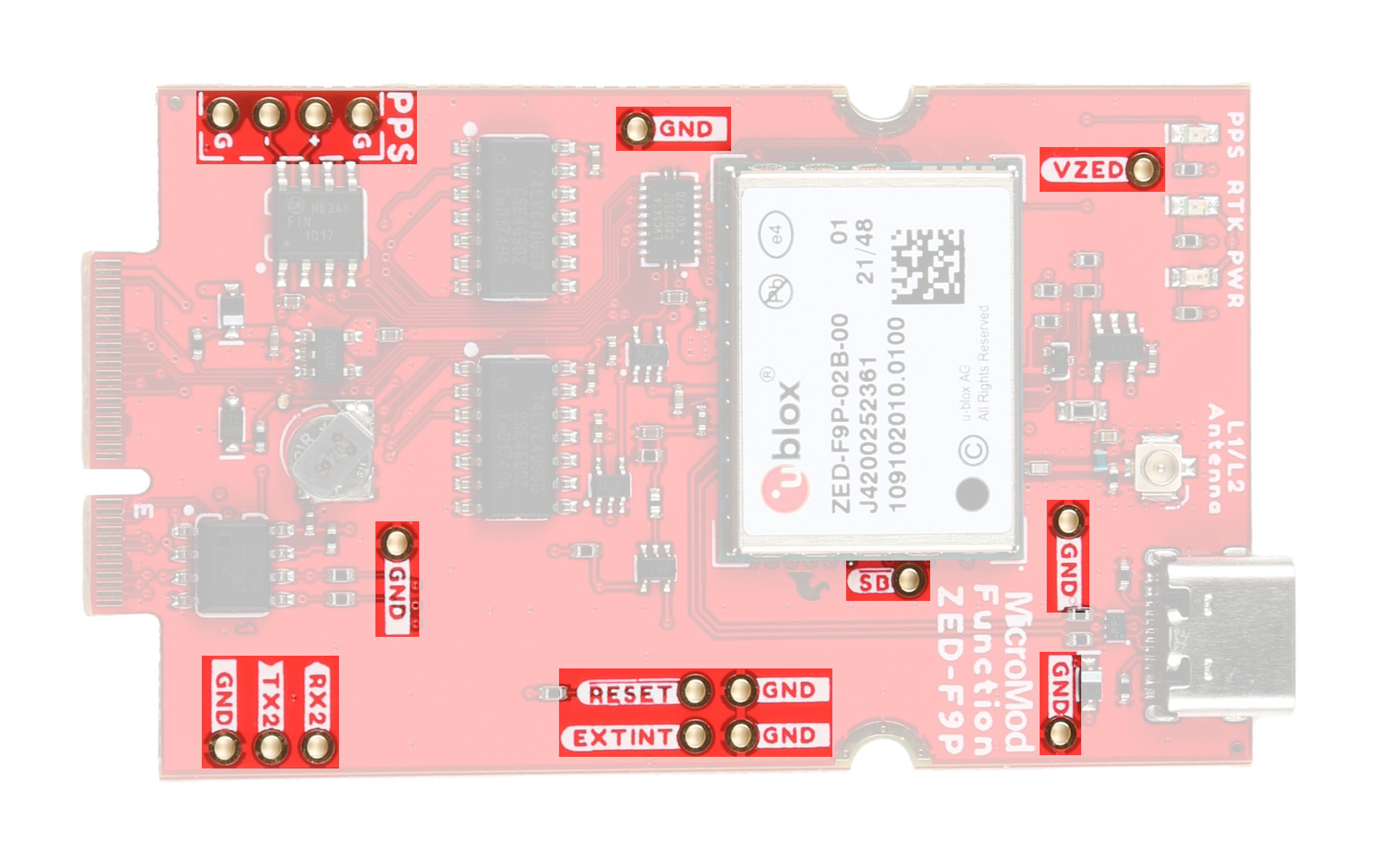
The list below outlines the labels and functionality of the PTH connections on the Function Board:
- PPS - The board translates the Pulse-Per-Second (PPS) output to a differential output routed to a pair of PTHs along with matching ground PTHs.
- RX2/TX2 - The ZED-F9P's secondary UART (RX2/TX2) along with a ground PTH.
- Reset - ZED-F9P reset pin.
- EXTINT - ZED-F9P external interrupt pin.
- SB - ZED-F9P SafeBoot pin.
- GND - Several Ground PTHs if needed.
LEDs
The GNSS Function Board - ZED-F9P has three LEDs labeled: PWR, PPS and RTK.
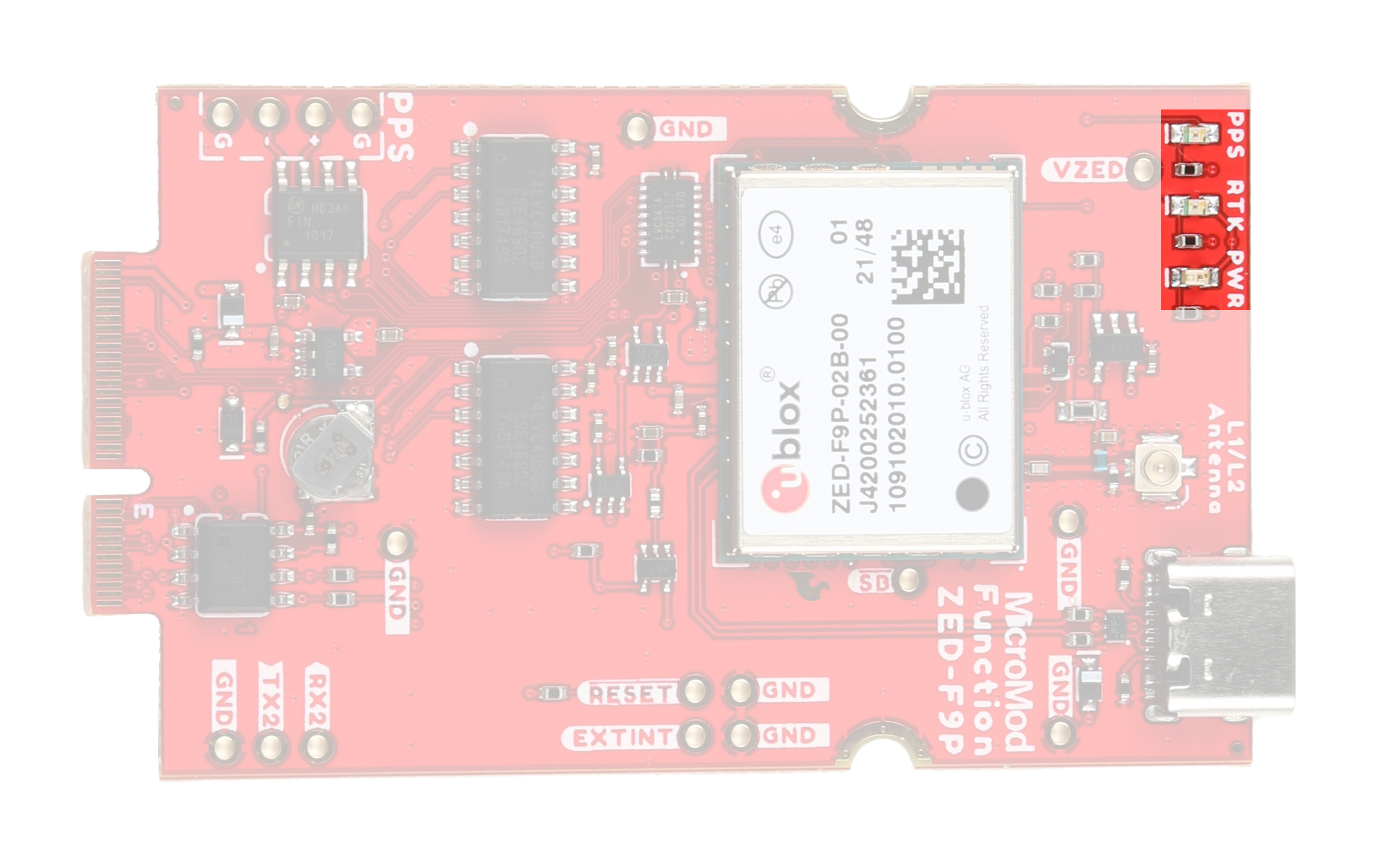
- PWR - Indicates when the ZED-F9P is powered.
- PPS - Tied to the Pulse Per Second pin and acts as a visual indicator to the ZED-F9P pulse per second signal.
- RTK - Indicates the status of the RTK lock.
Solder Jumpers
This board has nine solder jumpers. The table below outlines each jumper's label, default state, function and notes regarding their use:
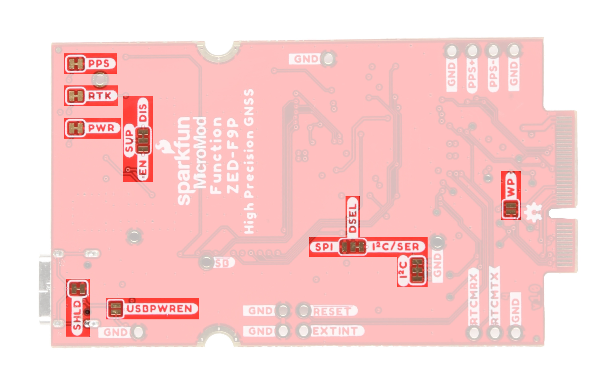
| Label | Default State | Function | Notes |
|---|---|---|---|
| USBPWREN | OPEN | Enables USB power to ZED-F9P. | Close to use the USB-C connector on the Function Board to power the ZED-F9P. |
| SHLD | CLOSED | USB-C shield control. | Open to disconnect the USB-C shield pin to the ground plane. |
| SUP | Disable | Antenna supervisor circuit control. | Disables the antenna supervisor circuit by default. Switch to EN side to enable the circuit. |
| DSEL | ZED-F9P interface selection. | I2C/Serial | Three pad jumper controls which communication interface the ZED-F9P uses. Can be set to I2C/Serial (Default) or SPI. |
| I2C | CLOSED | I2C pull up resistors | Three-way jumper pulling the SDA and SCL lines to 3.3V through a pair of 2.2kΩ resistors. Sever both traces to disable the pull up resistors. |
| WP | EEPROM Write Protection | OPEN | Close to clarification needed write protection on the EEPROM IC. |
| PWR | Power LED control. | CLOSED | Enables the ZED-F9P power indicator LED. Open to disable the LED. |
| PPS | PPS LED control. | CLOSED | Enables the ZED-F9P pulse per second LED. Open to disable the LED. |
| RTK | RTK LED control. | CLOSED | Enables the ZED-F9P RTK lock indicator LED. Open to disable the LED. |
MicroMod Pinout
This Function Board uses the following pins on a connected Processor Board:
- 3.3V & VCC
- Power enable
- SPI - ZED-F9P SPI
- I2C - ZED-F9P I2C and EEPROM
- UART RX1/TX1 (Slot 0) / UART RX2/TX2 (Slot 1) - ZED-F9P UART1
- CS0 (Slot 0) / CS1 (Slot 1) - ZED-F9P Chip Select
- D0 (Slot 0) / D1 (Slot 1) - ZED-F9P TX Ready
- PWM0 (Slot 0) / PWM1 (Slot 1) - ZED-F9P Pulse-Per-Second
- G0 (Slot 0) / G5 (Slot 1) - ZED-F9P Reset
- G1 (Slot 0) / G6 (Slot 1) - External Interrupt
- G2 (Slot 0) / G7 (Slot 1) - RTK Status
- G3 (Slot 0) / G8 (Slot 1) - Geofence Status
For the complete MicroMod Pinout and pins used by this function board, take a look at the tables below:
| AUDIO | UART | GPIO/BUS | I2C | SDIO | SPI0 | Dedicated |
| Function | Bottom Pin |
Top Pin |
Function | ||||||
|---|---|---|---|---|---|---|---|---|---|
| (Not Connected) | 75 | GND | |||||||
| 3.3V | 74 | 73 | G5 / BUS5 | ||||||
| RTC_3V_BATT | 72 | 71 | G6 / BUS6 | ||||||
| SPI_CS1# | SDIO_DATA3 (I/O) | 70 | 69 | G7 / BUS7 | |||||
| SDIO_DATA2 (I/O) | 68 | 67 | G8 | ||||||
| SDIO_DATA1 (I/O) | 66 | 65 | G9 | ADC_D- | CAM_HSYNC | ||||
| SPI_CIPO1 | SDIO_DATA0 (I/O) | 64 | 63 | G10 | ADC_D+ | CAM_VSYNC | |||
| SPI COPI1 | SDIO_CMD (I/O) | 62 | 61 | SPI_CIPO (I) | |||||
| SPI SCK1 | SDIO_SCK (O) | 60 | 59 | SPI_COPI (O) | LED_DAT | ||||
| AUD_MCLK (O) | 58 | 57 | SPI_SCK (O) | LED_CLK | |||||
| CAM_MCLK | PCM_OUT | I2S_OUT | AUD_OUT | 56 | 55 | SPI_CS# | |||
| CAM_PCLK | PCM_IN | I2S_IN | AUD_IN | 54 | 53 | I2C_SCL1 (I/O) | |||
| PDM_DATA | PCM_SYNC | I2S_WS | AUD_LRCLK | 52 | 51 | I2C_SDA1 (I/O) | |||
| PDM_CLK | PCM_CLK | I2S_SCK | AUD_BCLK | 50 | 49 | BATT_VIN / 3 (I - ADC) (0 to 3.3V) | |||
| G4 / BUS4 | 48 | 47 | PWM1 | ||||||
| G3 / BUS3 | 46 | 45 | GND | ||||||
| G2 / BUS2 | 44 | 43 | CAN_TX | ||||||
| G1 / BUS1 | 42 | 41 | CAN_RX | ||||||
| G0 / BUS0 | 40 | 39 | GND | ||||||
| A1 | 38 | 37 | USBHOST_D- | ||||||
| GND | 36 | 35 | USBHOST_D+ | ||||||
| A0 | 34 | 33 | GND | ||||||
| PWM0 | 32 | 31 | Module Key | ||||||
| Module Key | 30 | 29 | Module Key | ||||||
| Module Key | 28 | 27 | Module Key | ||||||
| Module Key | 26 | 25 | Module Key | ||||||
| Module Key | 24 | 23 | SWDIO | ||||||
| UART_TX2 (O) | 22 | 21 | SWDCK | ||||||
| UART_RX2 (I) | 20 | 19 | UART_RX1 (I) | ||||||
| CAM_TRIG | D1 | 18 | 17 | UART_TX1 (0) | |||||
| I2C_INT# | 16 | 15 | UART_CTS1 (I) | ||||||
| I2C_SCL (I/0) | 14 | 13 | UART_RTS1 (O) | ||||||
| I2C_SDA (I/0) | 12 | 11 | BOOT (I - Open Drain) | ||||||
| D0 | 10 | 9 | USB_VIN | ||||||
| SWO | G11 | 8 | 7 | GND | |||||
| RESET# (I - Open Drain) | 6 | 5 | USB_D- | ||||||
| 3.3V_EN | 4 | 3 | USB_D+ | ||||||
| 3.3V | 2 | 1 | GND | ||||||
| Description | Function | Bottom Pin |
Top Pin |
Function | Description |
|---|---|---|---|---|---|
| (Not Connected) | 75 | GND | |||
| - | 74 | 73 | 3.3V | Power Supply: 3.3-6V | |
| - | 72 | 71 | Power EN | Power Enable | |
| - | 70 | 69 | - | ||
| - | 66 | 65 | - | ||
| - | 64 | 63 | - | ||
| - | 62 | 61 | - | ||
| - | 60 | 59 | GEO_STAT | ZED-F9P Geofence Status Signal | |
| - | 58 | 57 | RTK_STAT | ZED-F9P RTK Lock Status Signal | |
| - | 56 | 55 | EXTINT | ZED-F9P External Interrupt | |
| - | 54 | 53 | RESET | ZED-F9P Reset | |
| - | 52 | 51 | PPS | ZED-F9P Pulse-Per-Second Signal | |
| - | 50 | 49 | CS | ZED-F9P Chip Select | |
| - | 48 | 47 | TX_READY | ZED-F9P UART TX Ready Signal | |
| - | 46 | 45 | GND | ||
| - | 44 | 43 | - | ||
| - | 42 | 41 | - | ||
| Write protection pin for the EEPROM. Pull low to enable. | EEPROM_WP | 40 | 39 | GND | |
| - | 38 | 37 | - | ||
| EEPROM I2C address configuration. | EEPROM_A0 | 36 | 35 | - | |
| EEPROM I2C address configuration. | EEPROM_A1 | 34 | 33 | GND | |
| EEPROM I2C address configuration. | EEPROM_A2 | 32 | 31 | Module Key | |
| Module Key | 30 | 29 | Module Key | ||
| Module Key | 28 | 27 | Module Key | ||
| Module Key | 26 | 25 | Module Key | ||
| Module Key | 24 | 23 | - | ||
| - | 22 | 21 | I2C_SCL | I2C - Clock Signal | |
| - | 20 | 19 | I2C_SDA | I2C - Data Signal | |
| - | 18 | 17 | - | ||
| - | 16 | 15 | RX | ZED RX | |
| - | 14 | 13 | TX | ZED TX | |
| - | 12 | 11 | - | ||
| - | 10 | 9 | - | ||
| - | 8 | 7 | POCI | SPI Peripheral Output/Controller Input. | |
| - | 6 | 5 | PICO | SPI Peripheral Input/Controller Output. | |
| - | 4 | 3 | SCK | SPI Clock Signal | |
| - | 2 | 1 | GND |
| Signal Group | Signal | I/O | Description | Voltage | Power | 3.3V | I | 3.3V Source | 3.3V |
|---|---|---|---|---|
| GND | Return current path | 0V | ||
| USB_VIN | I | USB VIN compliant to USB 2.0 specification. Connect to pins on processor board that require 5V for USB functionality | 4.8-5.2V | |
| RTC_3V_BATT | I | 3V provided by external coin cell or mini battery. Max draw=100μA. Connect to pins maintaining an RTC during power loss. Can be left NC. | 3V | |
| 3.3V_EN | O | Controls the carrier board's main voltage regulator. Voltage above 1V will enable 3.3V power path. | 3.3V | |
| BATT_VIN/3 | I | Carrier board raw voltage over 3. 1/3 resistor divider is implemented on carrier board. Amplify the analog signal as needed for full 0-3.3V range | 3.3V | |
| Reset | Reset | I | Input to processor. Open drain with pullup on processor board. Pulling low resets processor. | 3.3V |
| Boot | I | Input to processor. Open drain with pullup on processor board. Pulling low puts processor into special boot mode. Can be left NC. | 3.3V | |
| USB | USB_D± | I/O | USB Data ±. Differential serial data interface compliant to USB 2.0 specification. If UART is required for programming, USB± must be routed to a USB-to-serial conversion IC on the processor board. | |
| USB Host | USBHOST_D± | I/O | For processors that support USB Host Mode. USB Data±. Differential serial data interface compliant to USB 2.0 specification. Can be left NC. | |
| CAN | CAN_RX | I | CAN Bus receive data. | 3.3V |
| CAN_TX | O | CAN Bus transmit data. | 3.3V | |
| UART | UART_RX1 | I | UART receive data. | 3.3V |
| UART_TX1 | O | UART transmit data. | 3.3V | |
| UART_RTS1 | O | UART ready to send. | 3.3V | |
| UART_CTS1 | I | UART clear to send. | 3.3V | |
| UART_RX2 | I | 2nd UART receive data. | 3.3V | |
| UART_TX2 | O | 2nd UART transmit data. | 3.3V | |
| I2C | I2C_SCL | I/O | I2C clock. Open drain with pullup on carrier board. | 3.3V |
| I2C_SDA | I/O | I2C data. Open drain with pullup on carrier board | 3.3V | |
| I2C_INT# | I | Interrupt notification from carrier board to processor. Open drain with pullup on carrier board. Active LOW | 3.3V | |
| I2C_SCL1 | I/O | 2nd I2C clock. Open drain with pullup on carrier board. | 3.3V | |
| I2C_SDA1 | I/O | 2nd I2C data. Open drain with pullup on carrier board. | 3.3V | |
| SPI | SPI_PICO | O | SPI Peripheral Input/Controller Output. | 3.3V |
| SPI_POCI | I | SPI Peripheral Output/Controller Input. | 3.3V | |
| SPI_SCK | O | SPI Clock. | 3.3V | |
| SPI_CS# | O | SPI Chip Select. Active LOW. Can be routed to GPIO if hardware CS is unused. | 3.3V | |
| SPI/SDIO | SPI_SCK1/SDIO_CLK | O | 2nd SPI Clock. Secondary use is SDIO Clock. | 3.3V |
| SPI_PICO1/SDIO_CMD | I/O | 2nd SPI Peripheral Input/Controller Output. Secondary use is SDIO command interface. | 3.3V | |
| SPI_POCI1/SDIO_DATA0 | I/O | 2nd SPI Controller Output/Peripheral Input. Secondary use is SDIO data exchange bit 0. | 3.3V | |
| SDIO_DATA1 | I/O | SDIO data exchange bit 1. | 3.3V | |
| SDIO_DATA2 | I/O | SDIO data exchange bit 2. | 3.3V | |
| SPI_CS1/SDIO_DATA3 | I/O | 2nd SPI Chip Select. Secondary use is SDIO data exchange bit 3. | 3.3V | |
| Audio | AUD_MCLK | O | Audio master clock. | 3.3V |
| AUD_OUT/PCM_OUT/I2S_OUT/CAM_MCLK | O | Audio data output. PCM synchronous data output. I2S serial data out. Camera master clock. | 3.3V | |
| AUD_IN/PCM_IN/I2S_IN/CAM_PCLK | I | Audio data input. PCM syncrhonous data input. I2S serial data in. Camera periphperal clock. | 3.3V | |
| AUD_LRCLK/PCM_SYNC/I2S_WS/PDM_DATA | I/O | Audio left/right clock. PCM syncrhonous data SYNC. I2S word select. PDM data. | 3.3V | |
| AUD_BCLK/PCM_CLK/I2S_CLK/PDM_CLK | O | Audio bit clock. PCM clock. I2S continuous serial clock. PDM clock. | 3.3V | |
| SWD | SWDIO | I/O | Serial Wire Debug I/O. Connect if processor board supports SWD. Can be left NC. | 3.3V |
| SWDCK | I | Serial Wire Debug clock. Connect if processor board supports SWD. Can be left NC. | 3.3V | |
| ADC | A0 | I | Analog to digital converter 0. Amplify the analog signal as needed to enable full 0-3.3V range. | 3.3V |
| A1 | I | Analog to digital converter 1. Amplify the analog signal as needed to enable full 0-3.3V range. | 3.3V | |
| PWM | PWM0 | O | Pulse width modulated output 0. | 3.3V |
| PWM1 | O | Pulse width modulated output 1. | 3.3V | |
| Digital | D0 | I/O | General digital input/output pin. | 3.3V |
| D1/CAM_TRIG | I/O | General digital input/output pin. Camera trigger. | 3.3V | |
| General/Bus | G0/BUS0 | I/O | General purpose pins. Any unused processor pins should be assigned to Gx with ADC + PWM capable pins given priority (0, 1, 2, etc.) positions. The intent is to guarantee PWM, ADC and Digital Pin functionality on respective ADC/PWM/Digital pins. Gx pins do not guarantee ADC/PWM function. Alternative use is pins can support a fast read/write 8-bit or 4-bit wide bus. | 3.3V |
| G1/BUS1 | I/O | 3.3V | ||
| G2/BUS2 | I/O | 3.3V | ||
| G3/BUS3 | I/O | 3.3V | ||
| G4/BUS4 | I/O | 3.3V | ||
| G5/BUS5 | I/O | 3.3V | ||
| G6/BUS6 | I/O | 3.3V | ||
| G7/BUS7 | I/O | 3.3V | ||
| G8 | I/O | General purpose pin | 3.3V | |
| G9/ADC_D-/CAM_HSYNC | I/O | Differential ADC input if available. Camera horizontal sync. | 3.3V | |
| G10/ADC_D+/CAM_VSYNC | I/O | Differential ADC input if available. Camera vertical sync. | 3.3V | |
| G11/SWO | I/O | General purpose pin. Serial Wire Output | 3.3V |
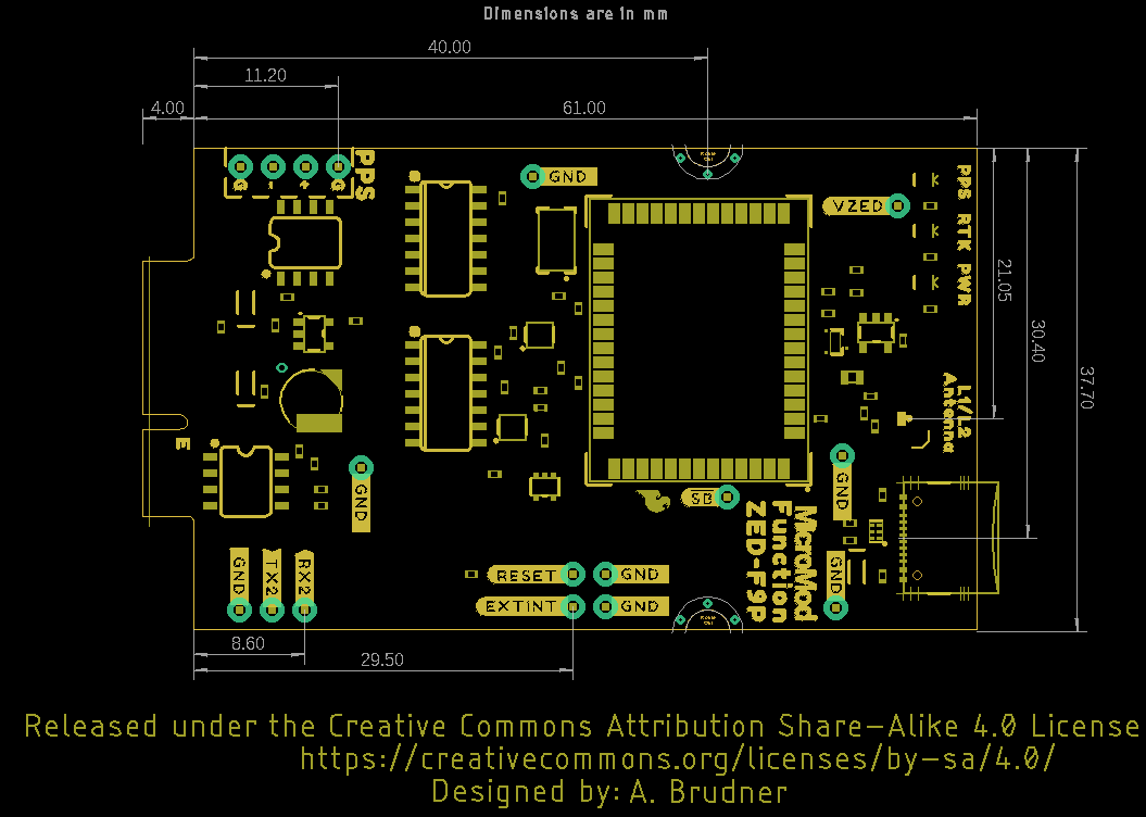
Board Dimensions
The board matches the MicroMod Function Board design specifications and measures 2.56" x 1.48" (65.02mm x 37.69mm) and the USB-C connector protrudes roughly 0.067" (1.70mm) from the edge of the board.
Hardware Assembly
If you're not familiar with assembling boards using the MicroMod connection system, head over to the MicroMod Main Board Hookup Guide for information on inserting and securing your MicroMod Processor and Function Boards to the Main Board:
MicroMod Main Board Hookup Guide
Antenna Connection
The antenna connection on this Function Board uses a u.Fl connector so an adapter like this is most likely needed. For tips on how to properly use a u.Fl connector, this tutorial can help.
Completed Assembly
With the Function and Processor Boards installed on a Main Board and the antenna and USB-C cables plugged in, your completed MicroMod assembly should look similar to the photo below:
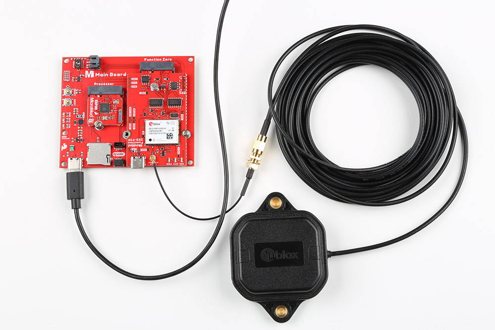
With the MicroMod assembly completed, we can move on to setting up the software and start getting location data from the ZED-F9P.
Software Installation
SparkFun u-blox Arduino Library
The SparkFun u-blox Arduino library enables the reading of all positional datums as well as sending binary UBX configuration commands over I2C. This is helpful for configuring advanced modules like the ZED-F9P but also the NEO-M8P-2, SAM-M8Q and any other u-blox module that use the u-blox binary protocol.
The SparkFun u-blox Arduino library can be downloaded with the Arduino library manager by searching 'SparkFun u-blox GNSS v3' or you can grab the zip here from the GitHub repository to manually install.
This SparkFun u-blox library really focuses on I2C because it's faster than serial and supports daisy-chaining. The library also uses the UBX protocol because it requires far less overhead than NMEA parsing and does not have the precision limitations that NMEA has.
In the next section we'll look at the first example included with the library to verify everything is working properly with the GNNS Function Board - ZED-F9P.
u-center Installation
For those who prefer to communicate directly with the ZED-F9P through the USB-C connector on the Function Board, head over to this tutorial to get started with u-center from u-blox:
Getting Started with U-Center for u-blox
Pin Connection Table
The table below helps show which pins the Function Board connects to depending on the slot it is connected to on a Main Board (Note: The Single Main Board connection is Slot 0):
| AUDIO | UART | GPIO/BUS | I2C | SDIO | SPI0 | Dedicated |
|
Function Board
Pin Name |
Main Board's
Processor Pin |
Slot 0 | Slot 1 |
|---|---|---|
| VCC | - | |
| 3.3V | - | |
| GND | - | |
| ZED_RX | TX1 | TX2 |
| ZED_TX | RX1 | RX2 |
| TX READY | D0 | D1 |
| CS | CS0 | CS1 |
| PPS | PWM0 | PWM1 |
| RST | G0 | G5 |
| INT | G1 | G6 |
| RTK | G2 | G7 |
| GEO | G3 | G8 |
Arduino Example
Example 1: Positional Accuracy
The first example in the SparkFun u-blox GNSS Arduino Library provides a quick test for position and accuracy. Navigate to the example by going to File > Examples > SparkFun u-blox GNSS v3 > ZED-F9P > Example1_GetPositionAccuracy.
Select your Board (in this case the SparkFun ESP32 MicroMod) and associated COM port. Upload the code and open the Arduino Serial Monitor with the baud set to 115200. Make sure the antenna has a clear view of the sky and give the ZED-F9P some time to get a satellite lock. Once the module gets a satellite lock the coordinates and accuracy should start to print out in the serial monitor window.
More Examples!
Now that you got it up and running, check out the other examples located in the ZED-F9P folder!
In order to get the most out of the ZED-F9P, you will need an RTCM correction source. Depending on your choice of Processor or other items in your setup, you may need a second ZED-F9P for a correction source. The following project tutorials guide you through setting up the ZED-F9P as a reference station or rover.
How to Build a DIY GNSS Reference Station
Setting up a Rover Base RTK System
Troubleshooting
u.Fl Tips
Unplugging the u.Fl adapter from the connector on the Function Board is tricky and improper removal can damage the connector or the board. For tips on using the u.Fl connector, check out this tutorial:
Three Quick Tips About Using U.FL
Position Lock Tips
Depending on your antenna choice and setup, you may experience issues getting your ZED-F9P to achieve a 3D lock. If you run into issues getting a lock, make sure the antenna has a clear view of the sky away from large objects such as buildings that may block the antenna view.
General Troubleshooting
If you need technical assistance and more information on a product that is not working as you expected, we recommend heading on over to the SparkFun Technical Assistance page for some initial troubleshooting.
If you don't find what you need there, the SparkFun Forums: MicroMod are a great place to find and ask for help. If this is your first visit, you'll need to create a Forum Account to search product forums and post questions.
Resources and Going Further
That's all for this tutorial. By now you should be able to start recording positional data with your completed MicroMod Main Board assembly using the GNSS Function Board - ZED-F9P. For more information, check out the following resources:
MicroMod GNSS Function Board Documentation:
ZED-F9P Documentation:
- Datasheet
- UBX and NMEA Protocol Manual
- Integration Manual
- Product Summary
- Release Notes - FW1.00
- Example RTCM output
- u-blox ECCN
MicroMod Documentation:
Looking for inspiration for a GNSS-RTK project? The following tutorials can help you get started:
Building an Autonomous Vehicle: The Batmobile
What is GPS RTK?
Setting up a Rover Base RTK System
How to Build a DIY GNSS Reference Station
Ready to get hands-on with GPS?
We've got a page just for you! We'll walk you through the basics of how GPS works, the hardware needed, and project tutorials to get you started.