Getting Started with the Artemis Development Kit
 Liquid Soulder, Member #1571936
 Hardware Overview
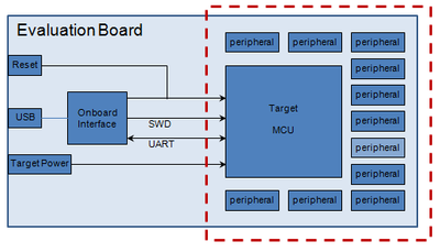
Board Operation /Functionality
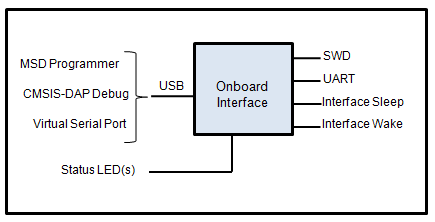
The functionality of this board can be broken up into 3 different systems: the USB interface, microcontroller (MCU), and the sensors and input/output (I/O) pins.
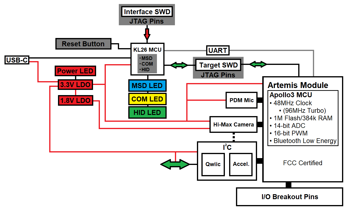
- MCU: The Artemis module serves as the brains of the board.
- All the pins on the Artemis module are utilized either by the sensors, camera connector, or I/O pins.
- Sensors and I/O Pins: There are two built-in sensors, with the option to add a camera, a Qwiic connector, and the breakout pins are relatively straight forward in their operation.
- The first sensor is the SPH0641LM4H-1 PDM microphone, that can be used for speach recognition.
- The second sensor is the LIS2DH12TR MEMS accelerometer, attached to the "Qwiic" I2C bus.
- The third psuedo-sensor is the camera connector, where an optional HM01B0 Himax camera can be attached.
- The I2C pin connections for the camera utilize the same bus as the "Qwiic" I2C bus.
- Any other Qwiic sensors attach to the same "Qwiic" I2C bus.
- The breakout pins all have their own dedicated connections to pads from the Artemis module. (i.e. The I/O pins do not share any connections to the sensors listed above.)
- USB Interface: The USB interface IC is the heart of the board's operation, which provides a link between the USB port and the Artemis module.
- Utilizing the provided DAPLink firmware, the IC enumerates as a composite device, with the following device classes:
- Mass Storage Device (MSD): Used to provide drag and drop programming.
- Human Interface Device (HID): Used for the debugging interface.
- Communication Port (COM): Used to provide a serial communication UART between the Artemis and the USB connection.
- Utilizing the provided DAPLink firmware, the IC enumerates as a composite device, with the following device classes:
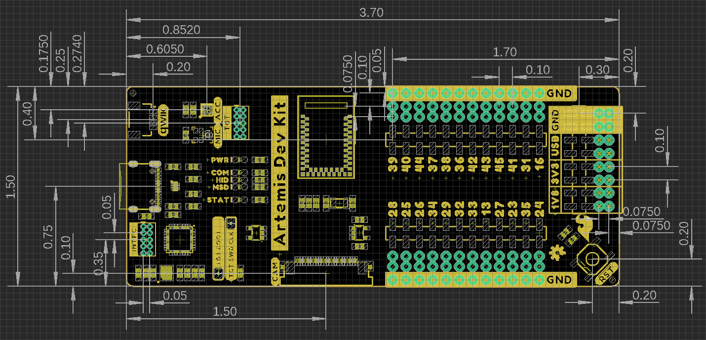
Board Dimensions
The board dimensions are illustrated in the drawing below. The primary highlight in the layout are the breakout pins, which provide both a .1" pitch spacing for headers and a .08" pitch spacing for IC-hooks, used by most logic analyzers.
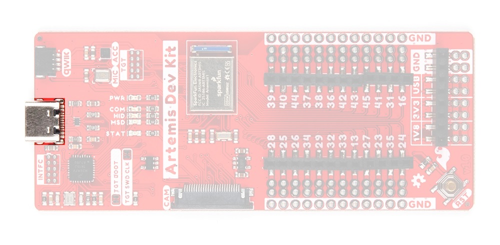
USB-C Connector
The USB connector is provided to power and program the board. For most users, it will be the primary programing interface for the Artemis module. A more detailed description of that functionality with the interface chip, is documented in the next section.
Interface Chip
Similar to the CH340, FTDI, or 32U4 chips on the SparkFun RedBoard or Arduino Uno; the MKL26Z128VFM4 Arm® Cortex®-M0+ MCU, from NXP, operates as an interface chip to the Artemis module. (*More advanced developers may recognize this DAPlink and the USB interface from the micro:bit.)
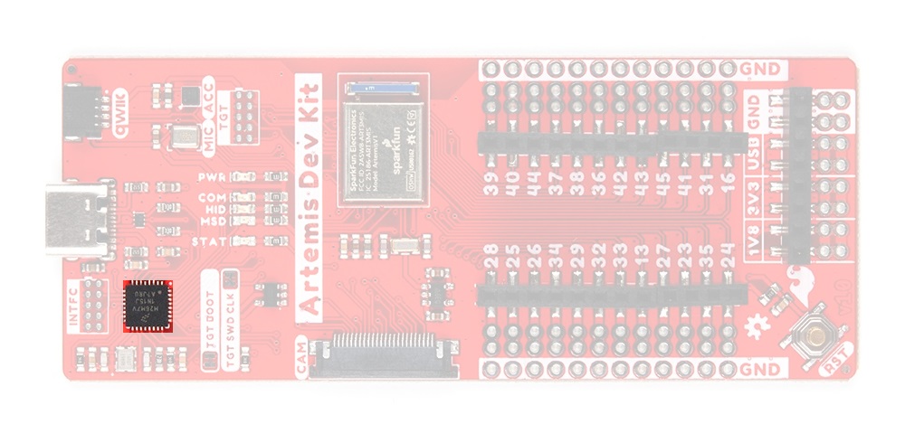
The MKL26Z128VFM4 microcontroller is connected to the software debug (SWD), reset, and UART pins of the Artemis module. To operate as an interface chip, it utilizes firmware from Arm® Mbed™ OS called Arm Mbed DAPLink (link), which a bootloader is pre-programmed through the intfc JTAG pins (see details in the Firmware section below). The firmware enables the board to enumerate as a composite USB device, when connected to a computer; this allows the interface chip to serve multiple functions:
- As a mass storage device (MSD), the interface chip provides drag and drop programming of a target MCU (i.e. the Aretemis module) and a USB bootloader for updating the firmware of the interface chip, itself.
- As a communications device class (CDC), the interface chip enumerates as a virtual com port and operates as a pass-through for serial communication between the target MCU to a PC.
- As a WEBUSB human interface device (HID), the interface chip functions as a bridge to the debug access port of the target MCU (the Aretemis module) and provides a CMSIS-DAP compliant debug channel.
Do I need to install any drivers?
If your computer is running Windows 10, Mac OSX or Linux and using DAPLink firmware version 0240 or later then drivers are not needed. If your computer is running Windows 7 (only), you will need to install the serial port driver. The board running DAPLink must be connected to your computer to install this driver.
Further instructions and details on installing the serial port driver can be found in the Mbed™ OS documentation. (*As the Mbed™ OS documentation is continually updated, so are the links. Therefore, users may find it useful to look under the Tutorials > Serial Communication section of the (updated) Mbed™ OS documentation for the serial port driver information.)
Firmware: Arm® Mbed™ DAPLink
DAPLink, previously known as CMSIS-DAP, is a standardized protocol for interfacing with an Arm® microcontroller's debug access port (DAP). It was developed as part of the Arm® Mbed™ OS and is maintained as an open source project. The DAPLink firmware runs on a secondary (interface) MCU that is attached to the (SWD or JTAG) debug port of the (target) Arm® MCU. On the Artemis DK, the MKL26Z128VFM4 inteface IC is the secondary MCU and the Artemis module is the target MCU, to be programmed or debugged.
Debug probe to the target MCU through its SWD port. (Photo courtesy of Arm® Mbed™.)
When a computer is connected to the USB interface, the DAPLink firmware enumerates the secondary MCU as a composite USB device; and implements a debug probe through the SWD or JTAG connection to the target MCU. As a result, the secondary MCU serves as bridge between the USB interface and the target MCU. Depending on the type of USB debug probe that is accessed, the following functions are all available to developers:
-
USB Drag and Drop Programming
DAPLink debug probes appear on the host computer as a USB disk. Program files in binary (.bin) and hex (.hex) formats can be copied onto the USB disk, which then programs them into the memory of the target system.- USB Mass Storage Device class (MSD)
- Drag and drop programming of the target chip (i.e. the Aretemis Module).
- USB bootloader for updating the interface firmware itself.
- Drag and drop programming of flash memory to update firmware.
- USB Mass Storage Device class (MSD)
-
USB Serial Port
The DAPLink debug probe also provides a USB serial port, which can be bridged through to a TTL UART on the target system. The USB serial port will appear on a Windows machine as aCOMport, or on a Linux machine as a/dev/ttyinterface.- USB Communications Device Class (CDC)
- For Serial Communication with the target chip.
- Virtual COM port for log, trace and terminal emulation.
- Serial passthrough from the target MCU to the PC. This is how messages get from the code you write onto the PC.
- USB Communications Device Class (CDC)
-
USB HID Debug Channel
The HID endpoint creates a tunnel to the target MCU's debug access port. This enables all the leading industry standard toolchains to program and debug the target system. Arm® Mbed™ has also developed pyOCD, an open-source, python based on-chip debugger and gdb-server that runs on Windows, Mac OSX and Linux.- USB Human Interface Device class (HID)
- WEBUSB HID - CMSIS-DAP compliant debug channel.
- This is useful if you want to use advanced debuggers like GDB or Keil to understand what’s happening (or not happening!) on the target MCU.
- Supported tools include:
- Keil MDK
- pyOCD
- USB Human Interface Device class (HID)
For more information on DAPLink, check out the documentation from Mbed™ OS:
- Debugging Methods for Arm® Mbed™ OS Applications
- DAPLink FAQ Page
- GitHub Repository
- DAPLink User's Guide
Users may also find these articles on the debug access port, informative:
Additional Resources: Since the DAPLink firmware operates similarly on the Micro:Bit, here are additional resources users can also reference.
Programming the Interface Chip
On the Artemis DK, the MKL26Z128VFM4 inteface IC is the secondary MCU and the Artemis module is the target MCU. Instructions for programming the MKL26Z128VFM4 microcontroller with the DAPLink firmware to operate as an interface chip, can be found in the SparkFun_Apollo3_AmbiqSuite_BSPs repository and the associated files are located in the artemis_dk/intfc directory. It is important to understand that the DAPLink consists of two functional parts, the underlying DAPLink bootloader and the DAPLink application interface firmware.
-
The DAPLink bootloader must first be initially flashed on a secondary (interface) MCU through its JTAG (or SWD) pins with a debug programmer. The bootloader configures the pin connections of the secondary MCU that allow it to interact with a target MCU (through the SWD connection of the target MCU) and enumerate as a storage device.
-
During production, the bootloader for the MKL26Z128VFM4 MCU is programmed through the
INTFCJTAG pins with a SEGGER J-Link (offset 0x00000000). This is also the only method to update or modify the bootloader.
Interface IC for the Artemis Development Kit and its JTAG pins. (Click to enlarge) -
To program the interface MCU, users will need one of the
kl26z_bl*.*bootloader files from the artemis_dk/intfc directory of the SparkFun_Apollo3_AmbiqSuite_BSPs repository. Any of the.hexor.binfiles (with or without aCRC) can be used. -
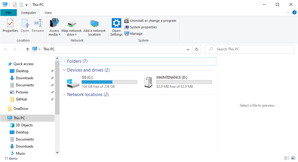
Once programmed, the bootloader will enumerate board as a mass storage device, labeled
MAINTENANCEwhen connected to a computer. The board will continue to appear theMAINTENANCEstorage device, while the secondary interface firmware hasn't been programmed.
The Artemis DK enumerating as a USB drive, namedMAINTENANCE. (Click to enlarge) -
When the board enumerates as the
MAINTENANCEstorage device, it is referred to as maintenance mode or bootloader mode.
-
-
Once the bootloader is programmed, the DAPLink interface firmware can be programmed on the interface MCU. The DAPLink interface firmware contains programming algorithms, specific for the target MCU. This works in conjunction with the underlying bootloader and allows the interface MCU to operate as a debug probe and access the target MCU, through its SWD (or JTAG) pins.
-
During production, the interface firmware, to target the Artemis module, is programmed on the MKL26Z128VFM4 MCU through the USB connection. On a computer, the interface firmware file is copied to the
MAINTENANCEstorage device.
The Artemis DK enumerating as a USB drive, namedMAINTENANCE. (Click to enlarge) -
The MKL26Z128VFM4 MCU can also be programmed through the
INTFCJTAG pins with a SEGGER J-Link. This method still requires the bootloader to be previously flashed and an offset must be used to avoid overwriting the bootloader.
Interface IC for the Artemis Development Kit and its JTAG pins. (Click to enlarge) -
To program the interface MCU, users will need one of the
kl26z_artemis_dk_if*.*interface firmware files from the artemis_dk/intfc directory of the SparkFun_Apollo3_AmbiqSuite_BSPs repository. Any of the.hexor.binfiles can be used. -
Once a secondary interface firmware is successfully programmed, the board will no longer appear as the
MAINTENANCEstorage device. The drive will instead be labeledARTEMISand will allow users to drag-and-drop compiled.binor.hexfiles to program the Artemis module.-
The maintenance mode can still be accessed, if the reset button is held down when the board is connected to the computer. Users can then, update the interface firmware with the same drag-and-drop process.
EnteringMAINTENANCEmode. (Click to enlarge)
-
The maintenance mode can still be accessed, if the reset button is held down when the board is connected to the computer. Users can then, update the interface firmware with the same drag-and-drop process.
-
When the board enumerates as the
ARTEMISstorage device, it is referred to as interface mode.
-
During production, the interface firmware, to target the Artemis module, is programmed on the MKL26Z128VFM4 MCU through the USB connection. On a computer, the interface firmware file is copied to the

Status LEDs
Attached to the interface chip are three indicator LEDs. These LEDs will flash according to the device class the Artemis DK enumerates as.
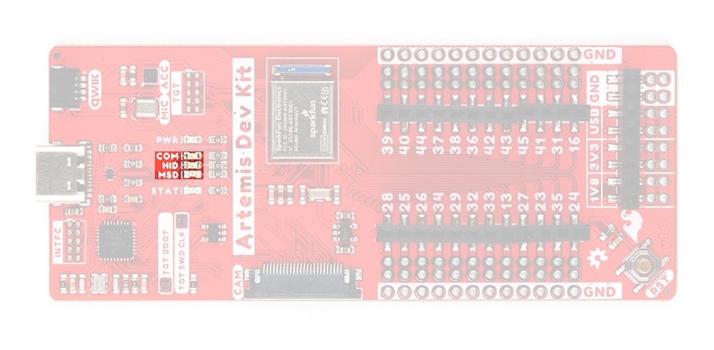
COM, HID, and MSD status LED indicators. (Click to enlarge) Maintenance Mode
Also known as bootloader mode, this mode accesses the bootloader and is used to update the interface firmware on the MKL26Z128VFM4, without using the JTAG pins. To enter maintenance mode, users need to hold down the RESET button, while plugging in the Artemis development kit into the computer. The board will enumerate as a mass storage device named MAINTENANCE.
MAINTENANCE. (Click to enlarge) Interface Mode
The interface mode is used to program the target MCU, the Artemis module. In this mode, the board will enumerate as a mass storage device, labeled ARTEMIS. Users can then drag and drop .bin or .hex files, which are written to the flash of the Artemis module.

ARTEMIS. (Click to enlarge) Virtual File System
The file system presented within the storage drive is virtual and not stored in flash memory, as it would on a USB flash disk. When a file is dropped onto the storage drive, the DAPLink firmware streams the data through the debug probe to program the target MCU; which is why the drive ejects itself after new files are written. Below are the virtual files for the Artemis DK:
DETAILS.TXT: This file contains diagnostic information and details on the version of DAPLink installed on the interface chip.ARTEMIS.HTML: This is a link to SparkFun's Artemis module webpage, to help users get started.FAIL.TXT: This file may appear, after a flashing error occurs; it will contain details on the cause of failure. Users can reference error.c file from the DAPLink repository to help diagnose the errors.
Why DAPLink? The reason for using this programming interface method was to provide full support for the Arduino BLE library, on the Artemis module.
Specifically, Mbed™ was needed to implement the Bluetooth functionality; and although DAPLink wasn't required for Mbed™, it was required to verify the pull request of our implementation of the Bluetooth functionality into Mbed™ OS. For more information about the reason Mbed™ was required to implement the Bluetooth functionality in the Arduino IDE, check out this article from Arduino, "Why we chose to build the Arduino Nano 33 BLE core on Mbed OS."
Reset Button
This button serves two functions: to reset the program running on the Artemis module and to enter into maintenance mode, for updating the firmware on the interface MCU.

Maintenance Mode
As mentioned earlier, maintenance mode is used to update the firmware on the MKL26Z128VFM4, without using the JTAG pins. To enter maintenance mode, users need to hold down the RESET button, while plugging in the Artemis development kit into the computer. The board will enumerate as a mass storage device named MAINTENANCE. Users can then drag and drop in the updated firmware .hex file.
MAINTENANCE mode. (Click to enlarge) Power
The Artemis Development Kit only requires 3.3V to power the board. However, the simplest method to power the board is with the USB-C connector. The power header consists of voltage supply pins, which are traditionally used as power sources for other peripheral hardware (like LEDs, potentiometers, and other circuits).
- 1.8V - A regulated 1.8V voltage source.
- Regulated from the 3.3V power.
- Used to power the camera connector.
- 3.3V - A regulated 3.3V voltage source.
- Regulated from the USB 5V power.
- Used to power the interface chip, Artemis module, Qwiic I2C bus (including the accelerometer and camera connector), and PDM microphone.
- USB - The input voltage from the USB-C connector, usually 5V.
- GND - The common ground or the 0V reference for the voltage supplies.

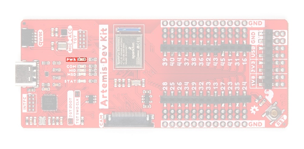
Power Status LED
The POWER LED will light up once 3.3V is supplied to the board; however, for most users, it will light up when 5V is supplied through the USB connection.
POWER status LED indicator. (Click to enlarge) Artemis Module
The Artemis module is the primary microcontoller on the Artemis Development Kit.
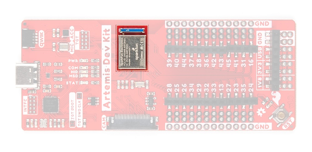
For details on the Artemis module, users should refer to the Designing with the SparkFun Artemis hookup guide. Additionally, users can reference the following resources for more technical information:
Designing with the SparkFun Artemis
Hardware Information:
- Artemis Integration Guide (PDF)
- Ambiq MCU Product Page
- Apollo3 DataSheet (PDF)
- Pin Function Map (PDF)
- Artemis GitHub Repository
Development Platforms:
Note: While most users will utilize the interface chip for drag-and-drop programming, the Artemis module can also be programmed through its JTAG or SWD pins. This might is useful for individuals developing and testing firmware that would be flashed directly onto the Artemis module, such as in production for commercial applications. For more details on programming, please check out our ARM Programming tutorial
ARM Programming
Artemis module and its JTAG pins on the Artemis Development Kit. (Click to enlarge)
Prior to programming the Artemis module, users will want to cut the TGT SWD CLK and TGT BOOT jumpers to isolate the Artemis module from the interface chip. Please feel free to reference our jumper modification tutorial for more instructions.

TGT SWD CLK and TGT BOOT jumpers on the Artemis Development Kit. (Click to enlarge)
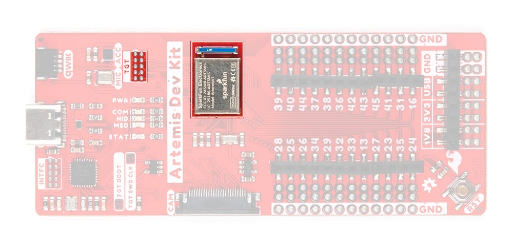
Breakout Pin Connections
The pins from the Artemis module are broken out into logical connections and available power connections are also broken out.
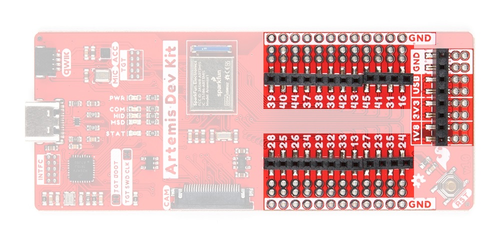
Note: The layout of the PTH connections for the breakout pins include both a .1" pitch spacing for headers and a .08" pitch spacing for IC-hooks, used by most logic analyzers.
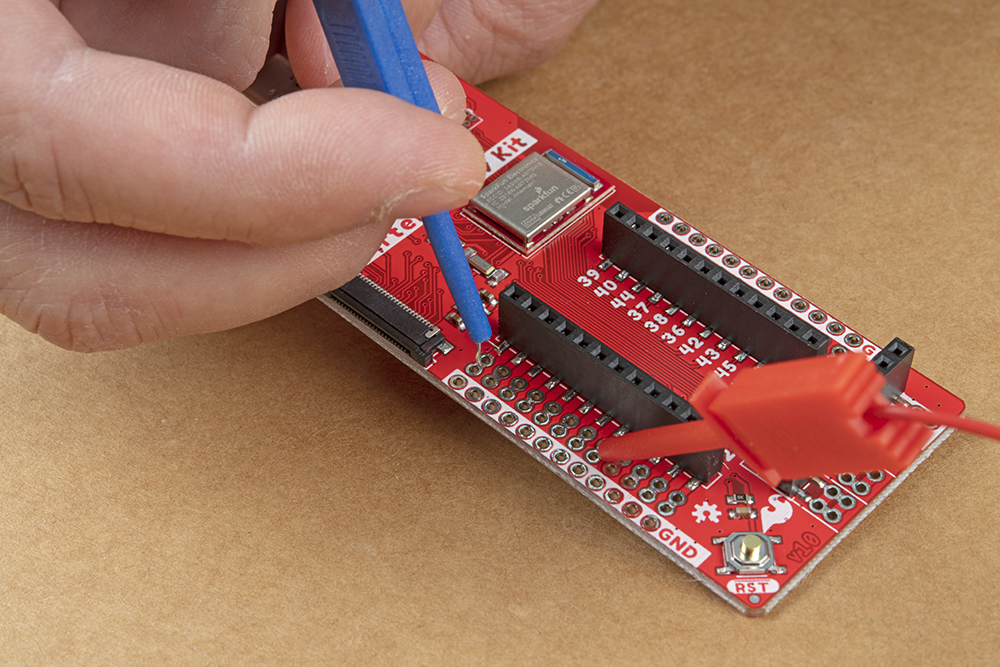
Connecting IC hooks to the Artemis Development Kit. (Click to enlarge)
Power Connections
The power header and pins aren't really I/O (Input/Output) connections for the microcontroller; however, they are pertinent to the board. (*For details on the pin connections to the peripherals, check out the next section.)
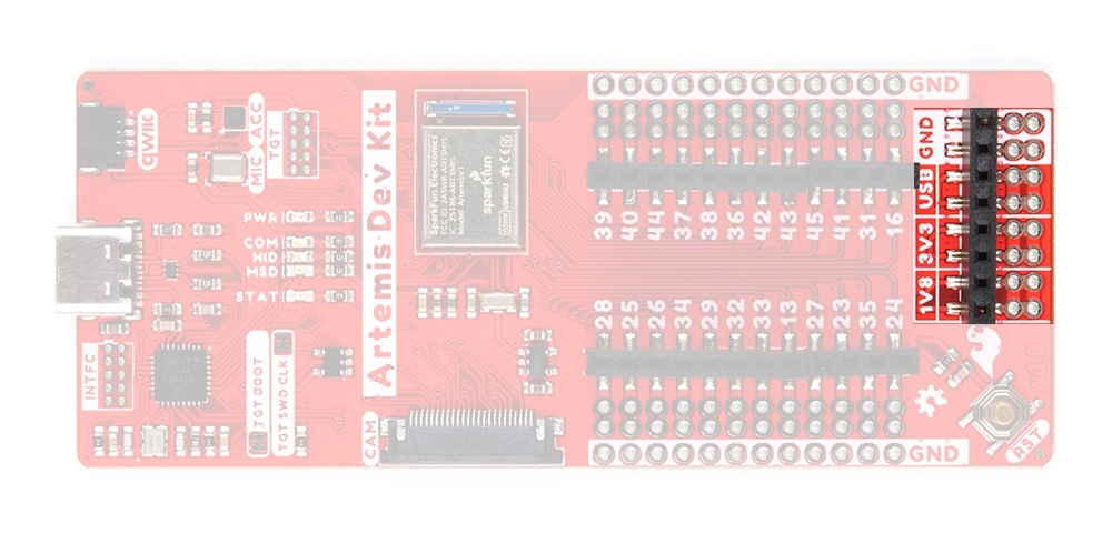
The power I/O mostly consists of voltage supply pins. These pins are traditionally used as power sources for other pieces of hardware (like LEDs, potentiometers, and other circuits).
- 1.8V - A regulated 1.8V voltage source.
- 3.3V - A regulated 3.3V voltage source.
- USB - The input voltage from the USB-C connector, usually 5V.
- GND - The common ground or the 0V reference for the voltage supplies.
I/O Pins
There are 24 I/O pins broken out on this board, which can be used as digital inputs to or outputs from the Artemis module.

All of the Artemis Development Kit pins are broken out to 0.1" spaced female headers (i.e. connectors). There are also two rows of breakout pins with .1" pitch spacing for headers; and a .08" pitch spacing to clip on IC-hooks, used by most logic analyzers. It is best practice to define the pinMode() (link) in the setup of each sketch (programs written in the Arduino IDE) for the pins used.
Input
When configured properly, an input pin will be looking for a HIGH or LOW state. Input pins are High Impedance and takes very little current to move the input pin from one state to another.
Output
When configured as an output the pin will be at a HIGH or LOW voltage. Output pins are Low Impedance: This means that they can provide a relatively substantial amount of current to other circuits.
Additional Functions
There are several pins that have special functionality in addition to general digital I/O. These pins and their additional functions are listed in the tabs below. For more technical specifications on the I/O pins, you can refer to the Apollo 3 datasheet and Artemis Integration Guide.
Analog Input Pins
The Artemis module offers a 14-bit ADC input for eight of the breakout I/O pins. This functionality is accessed in the Arduino IDE using the analogRead(pin) function. (*There is also a quick reference table for the available pin functionalities, labeled on the back of the board.)
Note: Be aware that the ADC input range is from 0 - 2V. Although connecting a sensor with an output to 3.3V is safe for the Artemis module, it will saturate the ADC at 2V.
Analog input pins on the Artemis Development Kit. (Click to enlarge)
analogRead() returns a 10-bit value. To change the resolution of the value returned by the analogRead() function, use the analogReadResolution(bits) function.
Note: To learn more about analog vs. digital signals, check out this great tutorial.
Analog vs. Digital
Pulse Width Modulation (PWM) Output Pins
The Artemis module provides 16-bit PWM output for eighteen of the breakout I/O pins. This is accessed in the Arduino IDE using the analogWrite(pin, value) function or the Servo library. (*There is also a quick reference table for the available pin functionalities, labeled on the back of the board.)

PWM pins on the Artemis Development Kit. (Click to enlarge)
Note: By default, in the Arduino IDE, analogWrite() accepts an 8-bit value. To change the resolution of the PWM signal for the analogWrite() function, use the analogWriteResolution(bits) function.
(*The PWM output is the result of the Artemis module's signal generator clock functionality and is not a true analog signal.)
Note: To learn more about pulse width modulation (PWM), check out this great tutorial.
Pulse Width Modulation
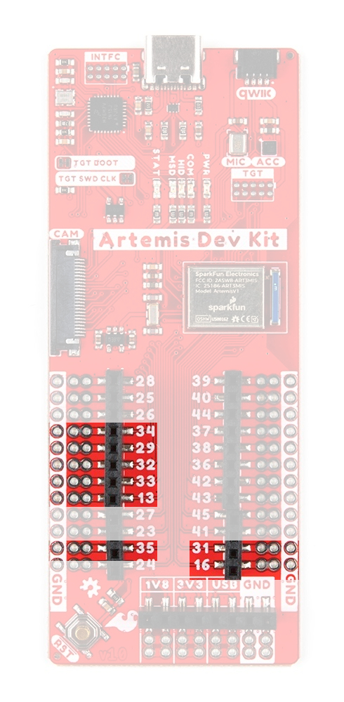
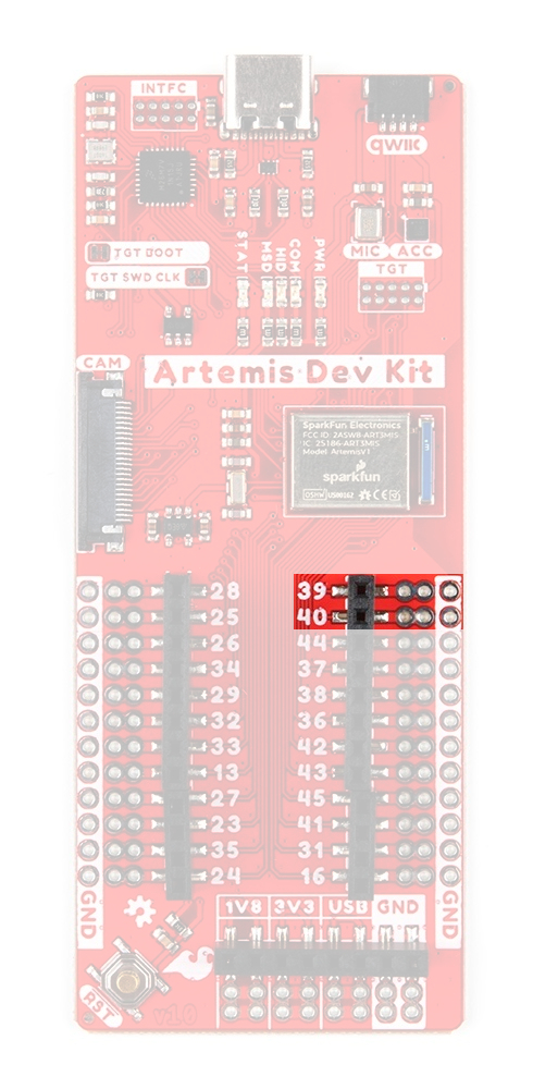
Serial Communication Pins
The Artemis module provides one dedicated UART port and two UART modules that can all function independently of each other. All of the breakout I/O pins, except pins 24, 32, 33, support this functionality. By default, the dedicated UART port to the USB connection is accessed through the Arduino IDE using the serial communication module. (*There is also a quick reference table for the available pin functionalities, labeled on the back of the board.)
TGT_RX and TGT_TX pins on UART0, to the USB connection. In order to utilize the serial communication on the breakout pins, users will need to create a custom serial port object and declare which pins to access.The breakout pins listed in the tables below can be utilized to create additional UART modules (UART0 and UART1). The available breakout pins are listed for each serial communication channel (TX and RX). For additional details on implementing the additional UART modules, please refer to the software guides (linked in the next section).
-
Only one of the available breakout pins can be selected for each communication channel; users cannot utilize multiple pins for a single communication channel. (i.e. The TX channel for
UART0can't operate on pins16and39simultaneously.) -
Likewise, some pins are available on both UART modules and therefore, can only operate with a single UART module at a time. (i.e. Pin
39can only operate as th TX channel forUART0orUART1; not both simultaneously.)
|
|
|
|---|---|
| TX |
16,
26,
28,
39,
41, or
44
|
| RX |
23,
27,
29,
31,
34,
40, or
45
|
Artemis DK serial communication pins for
UART0.
|
|
|
|---|---|
| TX |
35,
37,
39, or
42
|
| RX |
13,
25,
36,
38,
40, or
43
|
Artemis DK serial communication pins for
UART1.
Note: To learn more about serial communication, check out this great tutorial.
Serial Communication
SPI Communication
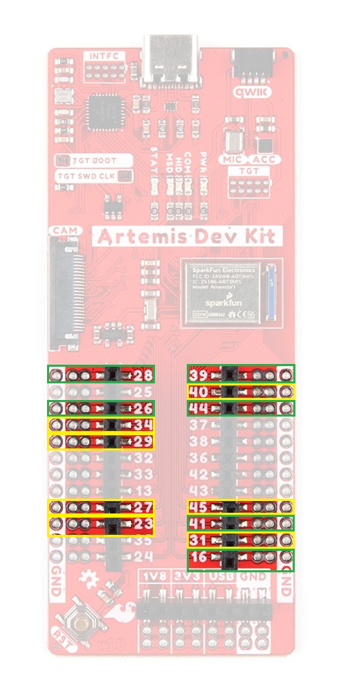
The Artemis module provides five I/O Master modules (IOM0 to IOM4); all of which, can function independently of each other as SPI or I2C bus.
IOM0is dedicated to the camera interface.IOM1is utilized by the Qwiic connector, accelerometer, and the I2C interface of the camera.IOM4is the default SPI bus that is accessed through the Arduino IDE using the SPI module.
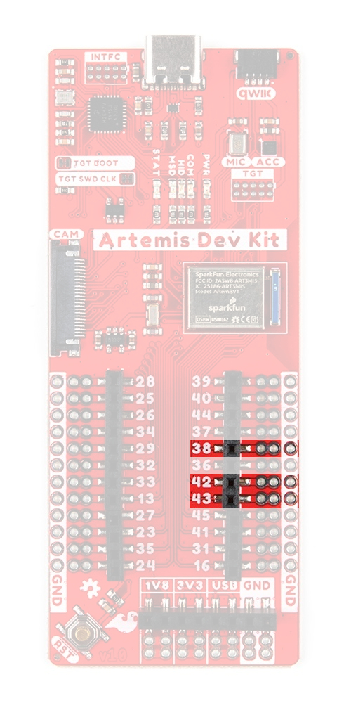
The breakout pins listed in the table below can be utilized to create SPI ports for each of the available IOM modules. By default, in the Arduino IDE, the SPI module is configured to utilize IOM4 (pins 39, 40, and 44). In order to utilize the other IOM modules as SPI ports, users will need to create a custom SPI object and declare which pins to access. For additional details on implementing SPI modules, please refer to the software guides (linked in the next section). (*There is also a quick reference table for the available pin functionalities, labeled on the back of the board.)
MOSI signal on a controller has been replaced with the title SDO. Please refer to this announcement on the decision to deprecate the MOSI/MISO terminology and transition to the SDO/SDI naming convention.
| IOM2 | IOM3 | IOM4 | |
|---|---|---|---|
| SCK | 27 |
42 |
39 |
| SDI or CIPO | 25 |
43 |
40 |
| SDO or COPI | 28 |
38 |
44 |
| CS | ANY |
ANY |
ANY |

IOM2
IOM3
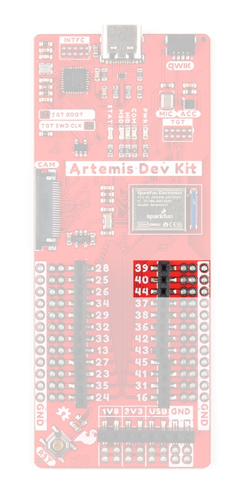
IOM4 (Default)
Note: To learn more about the serial peripheral interface (SPI) protocol, check out this great tutorial.
Serial Peripheral Interface (SPI)
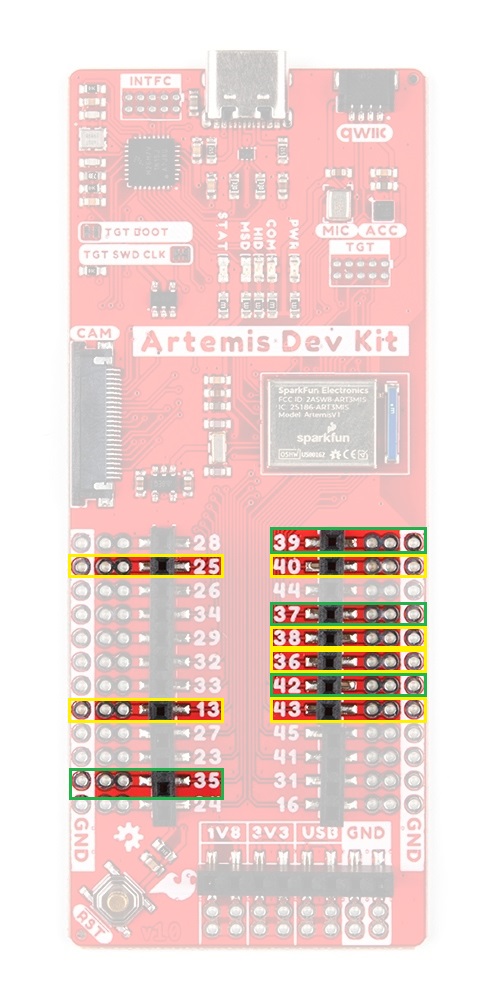
I2C Communication Pins
The Artemis module provides five I/O Master modules (IOM0 to IOM4); all of which, can function independently of each other as SPI or I2C bus.
IOM0is dedicated to the camera interface.IOM1is utilized by the Qwiic connector, accelerometer, and the I2C interface of the camera. It is the default I2C bus that is accessed through the Arduino IDE using the Wire module.IOM4is a peripheral IO master module.
The breakout pins listed in the table below can be utilized to create I2C ports for each of the available IOM modules. By default, in the Arduino IDE, the I2C module is configured to utilize IOM1 with the Qwiic connector. In order to utilize the other IOM modules as I2C ports, users will need to create a custom I2C object and declare which pins to access. For additional details on implementing I2C modules, please refer to the software guides (linked in the next section). (*There is also a quick reference table for the available pin functionalities, labeled on the back of the board.)
| IOM1 | IOM2 | IOM3 | IOM4 | |
|---|---|---|---|---|
| SCL | Qwiic Connector | 27 |
42 |
39 |
| SDA | Qwiic Connector | 25 |
43 |
40 |
IOM1
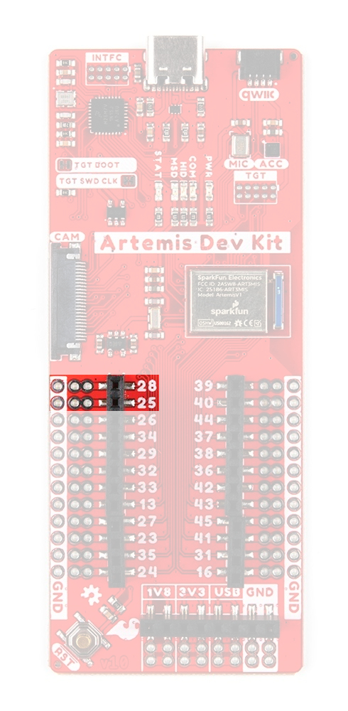
IOM2

IOM3
IOM4 (Default)
Pin Connections for Peripheral Devices
The following peripherals have dedicated pin connections.
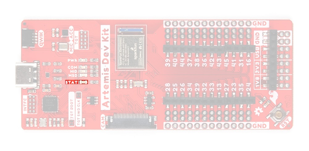
STAT LED
The STAT LED is typically used as a test LED to make sure that a board is working or for basic debugging. This indicator is connected to pin 23, which can also be referenced as D23 or LED1 in the Arduino IDE (*use LED1 in Mbed™ OS).
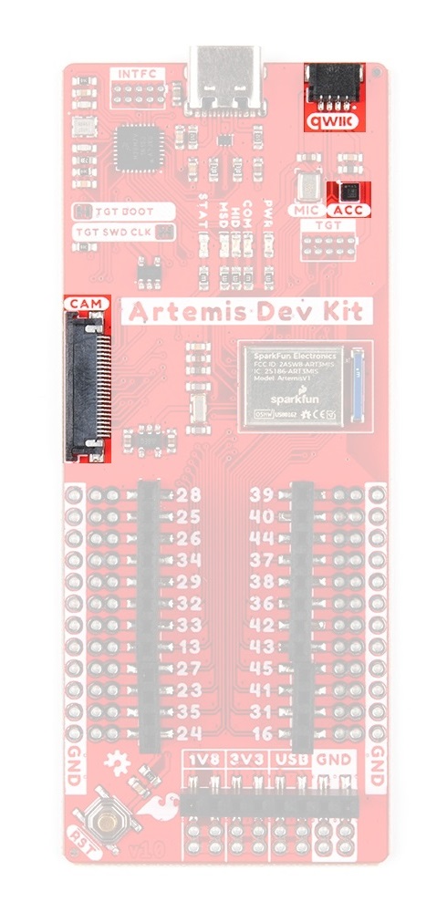
STAT LED indicator for the Artemis Development Kit. (Click to enlarge) Camera Connector
There is a 24-pin (FPC) camera connector intended for a Himax (HM01B0) camera, which can be used for visual recognition applications. Technical specifications for the camera can be found in the datasheet. The pin connections for the camera connector are detailed in the table below. (*Make sure to attach the camera in the correct orientation, as shown below.)

Camera connector on the Artemis Development Kit. (Click to enlarge)

Camera attached to the Artemis Development Kit. (Click to enlarge)
|
Pin Number
(Camera Connector) |
Connection Name |
Pad Number
(Artemis Module) |
|---|---|---|
4 |
AVDD |
3.3V |
10 |
IOVDD |
1.8V |
2 |
GND |
GND |
6 |
FVLD
VSYNC
|
D15 |
16 |
LVLD
HSYNC
|
D17 |
8 |
MCLK |
D18 |
17 |
PCLK |
D19 |
7 |
TRIG |
D14 |
18 |
INT |
D10 |
21 |
SCL |
D8 |
22 |
SDA |
D9 |
14 |
D0 |
D0 |
3 |
D1 |
D1 |
9 |
D2 |
D2 |
5 |
D3 |
D3 |
12 |
D4 |
D4 |
20 |
D5 |
D5 |
19 |
D6 |
D6 |
13 |
D7 |
D7 |
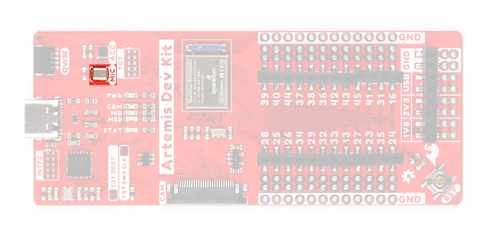
PDM Mic
There is a SPH0641LM4H-1 PDM microphone, which can be used for voice recognition applications. Technical specifications for the microphone can be found in the datasheet. The pin connections for the microphone are detailed in the table below.
| Connection | CLK |
DATA |
|---|---|---|
|
Pad Number
(Artemis Module) |
AD12 |
AD11 |
Note: In the Arduino IDE, a library is not required for users to utilize the PDM microphone. Additionally, there are exanples built-in with the installation of the board definitions. Users can access a list of examples from the File > Examples > PDM (under Examples for the Artemis Dev Kit) drop down menu.
Note: Currently, with the latest revision to the Arduino core, the examples will not compile due problems with the math library. For more details, users can track the issue in the GitHub repository.
Primary I2C Bus
An accelerometer and a Qwiic connector are attached to the primary I2C bus. The primary I2C bus for this board utilizes the pin connections, detailed in the table below:
| Connection | VDD |
GND |
SCL |
SDA |
|---|---|---|---|---|
|
Pad Number
(Artemis Module) |
3.3V | GND | D8 |
D9 |
Accelerometer
There is an LIS2DH12 3-axis accelerometer, which can be used for gesture recognition. Technical specifications for the accelerometer can be found in the datasheet.
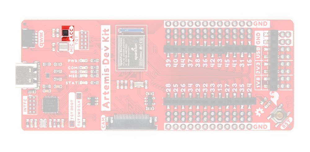
Note: In the Arduino IDE, users can utilize the SparkFun LIS2DH12 Arduino Library. Also, the orientation of the sensor's axes is labeled on the back of the board.
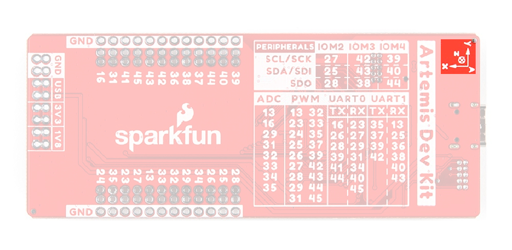
Silk marking the orientation of the accelerometer's axes, in reference to the Artemis Development Kit. (Click to enlarge)
Qwiic Connector
A Qwiic connector is provided for users to seamlessly integrate with SparkFun's Qwiic Ecosystem.
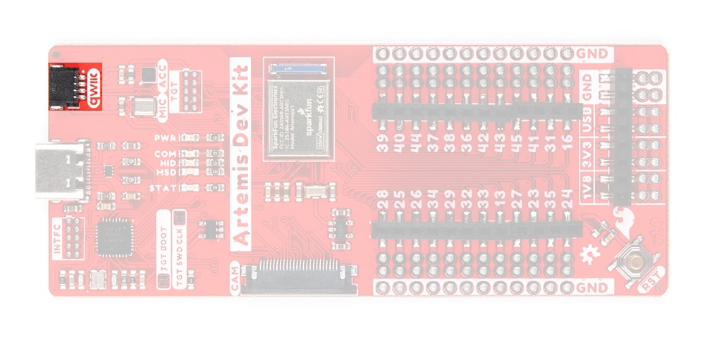
What is Qwiic?
The Qwiic system is intended a quick, hassle-free cabling/connector system for I2C devices. Qwiic is actually a play on words between "quick" and I2C or "iic".
Features of the Qwiic System
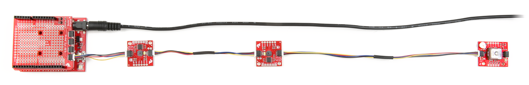
Keep your soldering iron at bay.
Cables plug easily between boards making quick work of setting up a new prototype. We currently offer three different lengths of Qwiic cables as well as a breadboard friendly cable to connect any Qwiic enabled board to anything else. Initially you may need to solder headers onto the shield to connect your platform to the Qwiic system but once that’s done it’s plug and go!
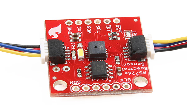
Qwiic cables connected to Spectral Sensor Breakout
Minimize your mistakes.
How many times have you swapped the SDA and SCL wires on your breadboard hoping the sensor will start working? The Qwiic connector is polarized so you know you’ll have it wired correctly, every time, from the start.
The PCB connector is part number SM04B-SRSS (Datasheet) or equivalent. The mating connector used on cables is part number SHR04V-S-B or equivalent. This is a common and low cost connector.
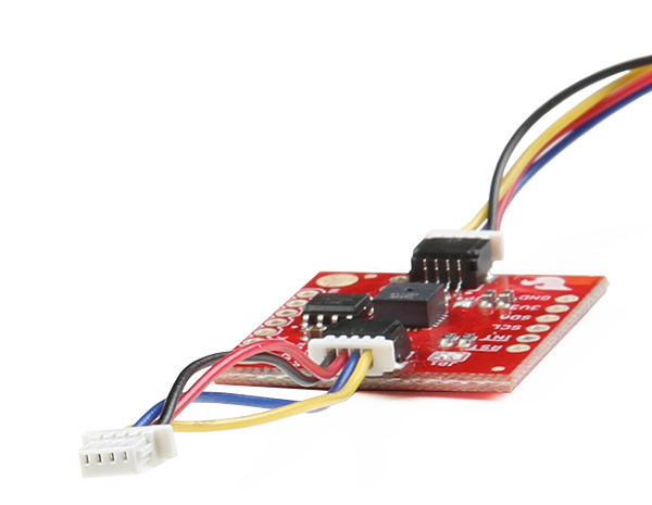
1mm pitch, 4-pin JST connector
Expand with ease.
It’s time to leverage the power of the I2C bus! Most Qwiic boards will have two or more connectors on them allowing multiple devices to be connected.