Dialog ULP WiFi DA16200 R3 Shield Hookup Guide
Hardware Overview
There's a lot to cover with this board. Let's get started!
DA16200
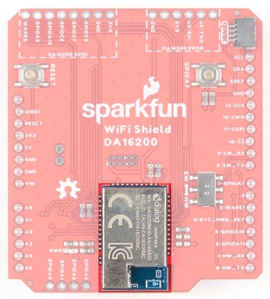
At the heart of this board is the DA16200 from Dialog - a fully integrated Wi-Fi® module with ultra-low power consumption, 40 MHz crystal oscillator, 32.768 KHz RTC clock, RF Lumped RF filter, 4 M-byte flash memory, and an onboard chip antenna. This chip is chock full of features - for more information, refer to the datasheet.
Power
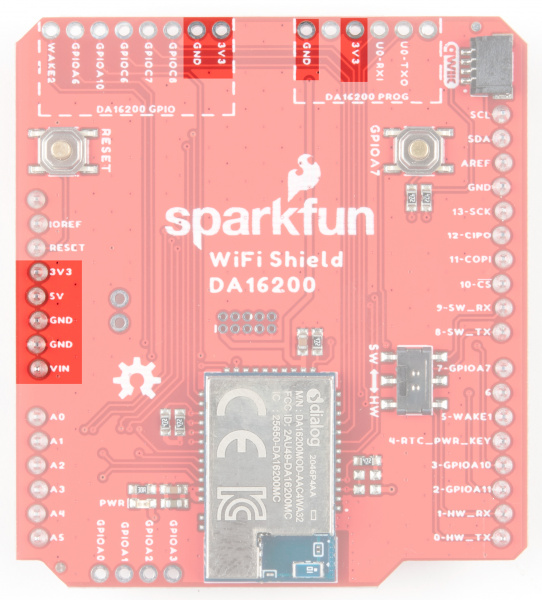
Power is available via a number of pins on the shield.
Wake
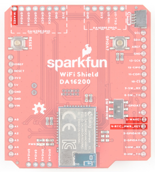
Integral to the ultra low power functionality is the wake-up controller. It is designed to wake up the DA16200 from a sleep mode by an external signal that selects either the rising edge or the falling edge on either WAKE1 or WAKE2. The RTC_PWR_KEY is used to enable the RTC block and switch between the various sleep modes. See the datasheet for more information.
Current Draw in Low Power Modes
UART
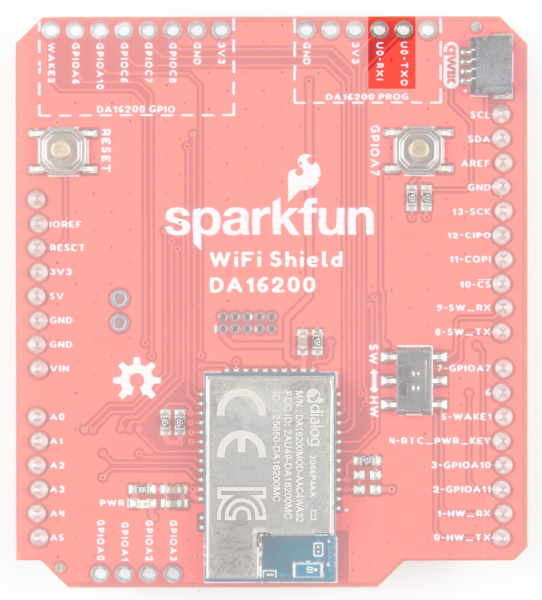
The DA16200 module has two UART interfaces. UART0 is used for updating the firmware to module, and UART1 is used for sending AT commands.
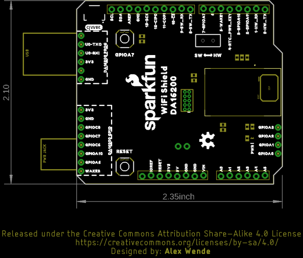
UART0 for the Dialog module sits at the top of the board.
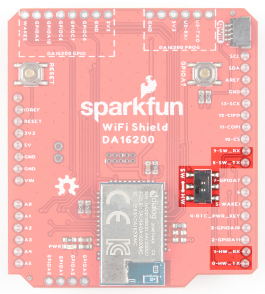
UART1 is used for sending AT commands and is routed through a switch to communicate through either the hardware UART pins D0/D1 for RX/TX, or software UART through D9/D8 for RX/TX.
SPI
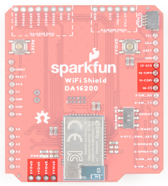
SPI functionality is found on pins 10-13 on the right side of the board. If you wish to bypass the SPI pins and instead use the ADC on GPIOA0-GPIOA3, there are jumpers on the back of the board to accomplish this. Refer to the Jumpers section below for more information.
DA16200 GPIO
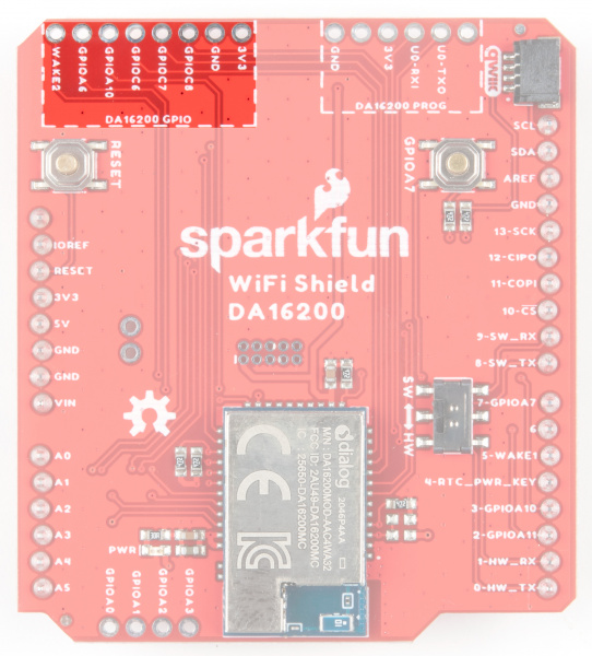
General purpose IO pins for the Dialog module are available at the top of the board.
Qwiic Connector
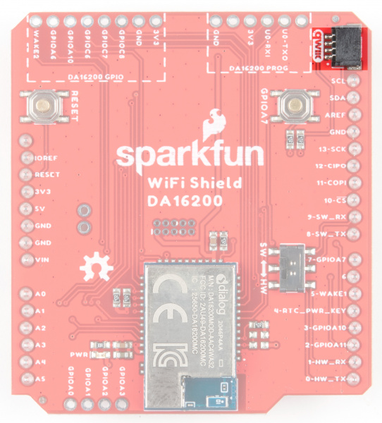
A Qwiic connector is provided such that if you have an older RedBoard without a Qwiic connector, you can still add on a Qwiic sensor of your choice. Or you can use both the existing Qwiic connector on your RedBoard as well as the Qwiic connector on your shield. The RedBoard itself acts as the I2C controller. If you need help choosing a Qwiic sensor, check out our Qwiic Ecosystem.
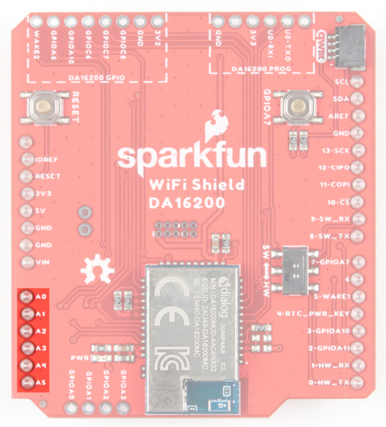
Pins A0-A5
These pins are present on the board, but are not routed to anything on the shield.
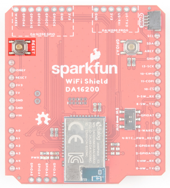
Buttons
A general reset button is located on the upper left side of the board.
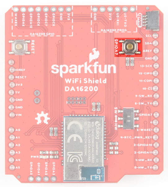
Pressing and holding GPIOA7 will perform a factory reset, which clears configurations that might have been saved to the module.
Jumpers
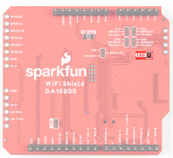
JP1
Cutting this jumper removes power from the LED on the front of the board.
JP2
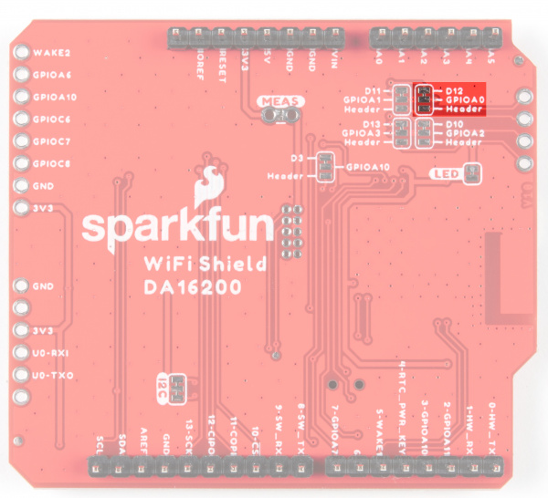
SPI CIPO is the default functionality for this shield. Cutting this jumper and closing the jumper between GPIOA0 and Header selects for GPIO A0 (Analog to Digital Converter functionality for Dialog Chip).
JP3
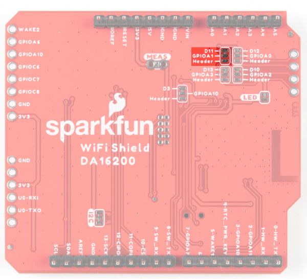
SPI COPI is the default functionality for this shield. Cutting this jumper and closing the jumper between GPIOA1 and Header selects for GPIO A1 (Analog to Digital Converter functionality for Dialog Chip).
JP4
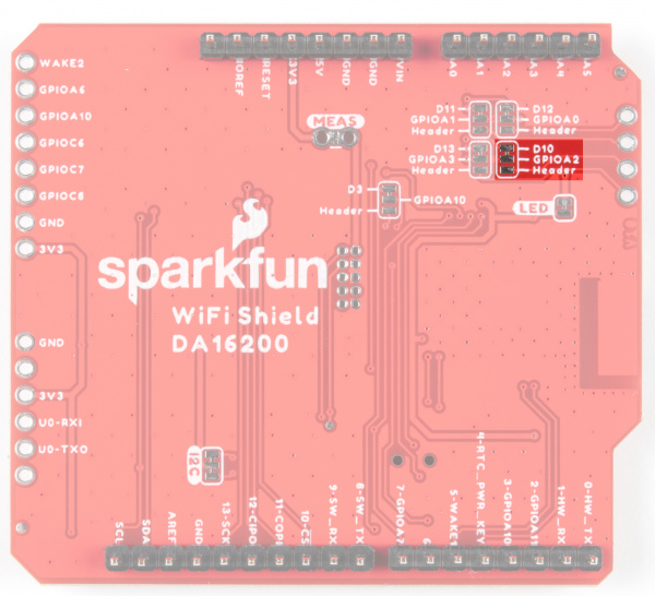
SPI CS is the default functionality for this shield. Cutting this jumper and closing the jumper between GPIOA2 and Header selects for GPIO A2 (Analog to Digital Converter functionality for Dialog Chip).
JP5
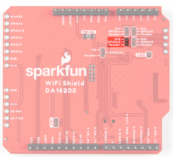
SPI SCK is the default functionality for this shield. Cutting this jumper and closing the jumper between GPIOA3 and Header selects for GPIO A3 (Analog to Digital Converter functionality for Dialog Chip).
JP6
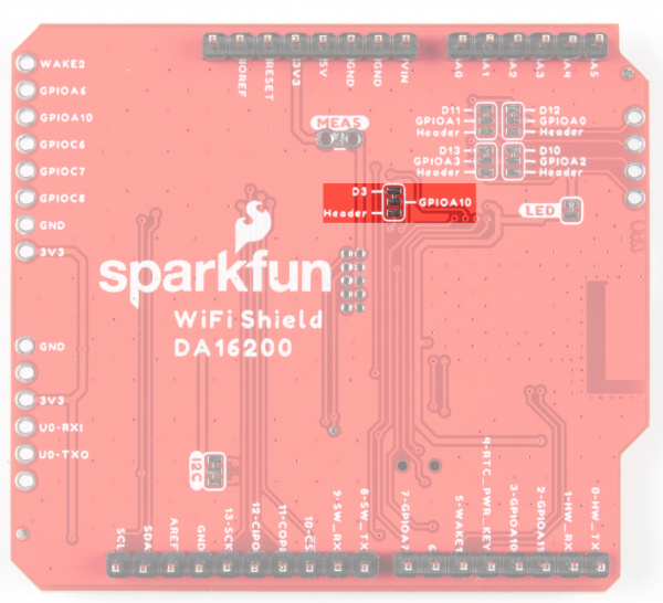
Selects SPI Interrupt to Arduino (default) or PWM to GPIO header
Current Measurement Jumper
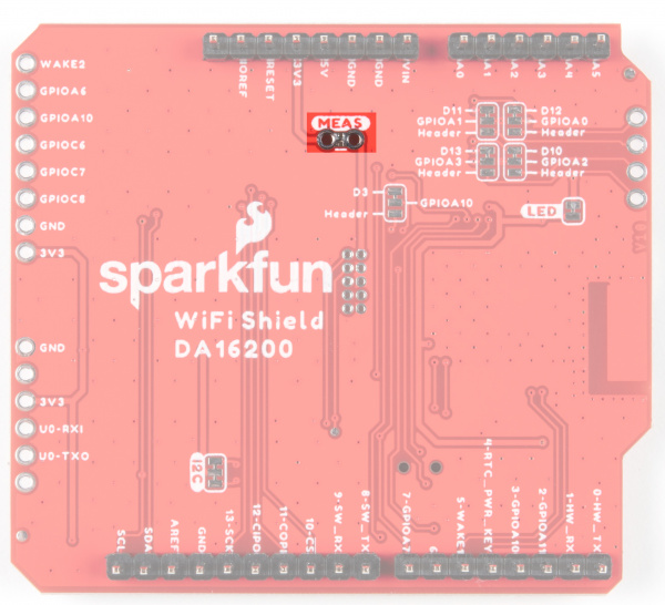
To enable measurements and to isolate the power hungry devices, we've added a NC (normally closed) jumper. By cutting the jumper on the back of the board, the VDD trace to the module is interrupted. Soldering in a male jumper or wires into the accompanying holes will give you the ability to insert a current meter and precisely monitor how much current your application is consuming.
I2C Jumper
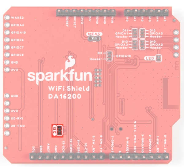
Cutting this jumper will disable the pull up resistors on the bus.
JTAG
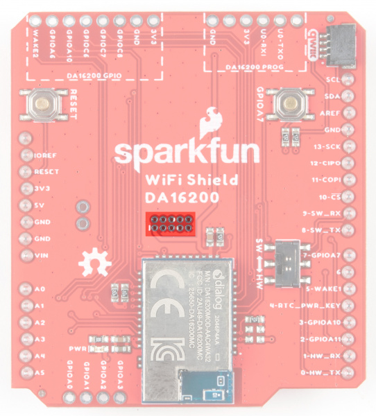
An unpopulated JTAG footprint is available for more advanced users who need breakpoint level debugging. We recommend checking out our JTAG section for the compatible male header and a compatible JTAG programmer and debugger.
