1W LoRa MicroMod Function Board Hookup Guide
 Nate, santaimpersonator
Hardware Overview
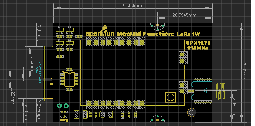
Board Dimensions
The overall board dimensions are roughly 65 x 35 mm with an approximate 6 mm protrusion of the RP-SMA antenna connector.
M.2 Edge Connector and Screw Slots
Like other function and processor boards, there is a polarized M.2 edge connector, which provides a standardized electrical connection. The attachment points for the screws prevent users from connecting a processor board into a function board slot and vice-versa.
Power
There is a power status LED to help make sure that your LoRa function board is getting (5V) power. Power is provided through the (MicroMod) M.2 edge connector. The LoRa module is meant to run on 5V with 3.3V logic levels. A jumper is available on the back of the board to remove power to the LED for low-power applications (see the Jumpers section below).
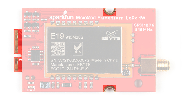
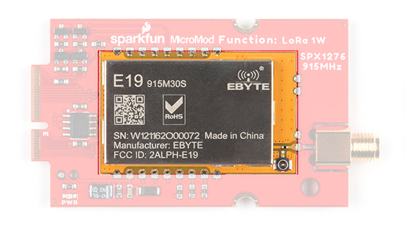
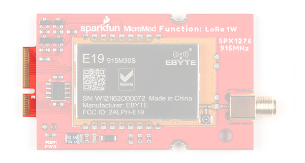
E19-915M30S LoRa Module
The Chengdu Ebyte E19-915M30S RF transceiver module is a 1W 915MHz LoRa module, based on the SX1276 from Semtech. It is FCC, CE, and RoHS certified and has been tested up to a range of 10km by the manufacturer. PLease refer to the datasheet for more details.
- Global license free ISM 915MHz band
- 1W maximum transmission power
- Software multi-level adjustable
- 256Byte FIFO data buffer
SX1276
The E19-915M30S transceiver is based on the SX1276 chip from Semtech. Please refer to the datasheet for more details.
| Part Number | SX1276 |
|---|---|
| Frequency Range | 137 - 1020 MHz |
| Spreading Factor | 6 - 12 |
| Bandwidth | 7.8 - 500 kHz |
| Effective Bitrate | .018 - 37.5 kbps |
| Est. Sensitivity | -111 to -148 dBm |
| Characteristic | Description |
|---|---|
| Operating Voltage | 3.3 - 5.5 V |
| Current Consumption | 630 mA (TX)) 23 mA (RX)) 3 µA (Sleep) |
| Operating Temperature | -40 - 85 °C |
| Operating Humidity[1] | 10 - 90% |
| Communication Interface | SPI (0 - 10 Mbps) |
| Logic Level | 3.3 V |
| Frequency Range | 900 - 931 MHz |
| Transmit Power | 28.5 - 30 dBm (max) |
| Modulation | LoRa, FSK, GFSK, MSK, GMSK, OOK |
| Data Rate |
FSK: 1.2 - 300 kbps
LoRa: 0.018 - 37.5 kbps |
| Antenna Impedance | 50 Ω |
Pin Connections
Below is a table of the pin connections available on the E19-915M30S RF transceiver module. However, not all the pins listed are utilized by the LoRa function board (see the Function Board Pinout Table section below).
| Pin # | Pin Name | I/O Direction | Pin Description |
| 1 | GND | Ground | |
| 2 | DIO5 | Input/Output | Configurable IO port(Please refer to the SX1276 datasheet). |
| 3 | DIO4 | Input/Output | Configurable IO port(Please refer to the SX1276 datasheet). |
| 4 | DIO3 | Input/Output | Configurable IO port(Please refer to the SX1276 datasheet). |
| 5 | DIO2 | Input/Output | Configurable IO port(Please refer to the SX1276 datasheet). |
| 6 | DIO1 | Input/Output | Configurable IO port(Please refer to the SX1276 datasheet). |
| 7 | DIO0 | Input/Output | Configurable IO port(Please refer to the SX1276 datasheet). |
| 8 | RST | Input | Reset |
| 9 | GND | Ground | |
| 10 | GND | Ground | |
| 11 | VCC | Input | Power supply: 4.75~5.5V (Ceramic filter capacitoris advised to add) |
| 12 | SCK | Input | SPI - Clock Signal |
| 13 | MISO | Output | SPI - Data from Peripheral Device |
| 14 | MOSI | Input | SPI - Data to Peripheral Device |
| 15 | NSS | Input | SPI - Chip Select |
| 16 | TXEN | Input | Radio frequency switch control, make sure the TXEN pin is in high level, RXEN pin is in low level when transmitting. |
| 17 | RXEN | Input | Radio frequency switch control, make sure the RXEN pin is in high level, TXEN pin is in low level when receiving. |
| 18 | GND | Ground | |
| 19 | ANT | Antenna | |
| 20 | GND | Ground | |
| 21 | GND | Ground | |
| 22 | GND | Ground |
MicroMod Edge Connector
The MicroMod M.2 edge connector provides a standardized interface for the pin connection of a function board.
Function Board Pinout Table
The tables below outline the pin on the M2. edge connector and their functions.
| AUDIO | UART | GPIO/BUS | I2C | SDIO | SPI0 | Dedicated |
| Functions | Bottom Pin |
Top Pin |
Functions | ||||||
|---|---|---|---|---|---|---|---|---|---|
| (Not Connected) | 75 | GND | |||||||
| 3.3V | 74 | 73 | G5 / BUS5 | ||||||
| RTC_3V_BATT | 72 | 71 | G6 / BUS6 | ||||||
| SPI_CS1# | SDIO_DATA3 (I/O) | 70 | 69 | G7 / BUS7 | |||||
| SDIO_DATA2 (I/O) | 68 | 67 | G8 | ||||||
| SDIO_DATA1 (I/O) | 66 | 65 | G9 | ADC_D- | CAM_HSYNC | ||||
| SPI_CIPO1 | SDIO_DATA0 (I/O) | 64 | 63 | G10 | ADC_D+ | CAM_VSYNC | |||
| SPI COPI1 | SDIO_CMD (I/O) | 62 | 61 | SPI_CIPO (I) | |||||
| SPI SCK1 | SDIO_SCK (O) | 60 | 59 | SPI_COPI (O) | LED_DAT | ||||
| AUD_MCLK (O) | 58 | 57 | SPI_SCK (O) | LED_CLK | |||||
| CAM_MCLK | PCM_OUT | I2S_OUT | AUD_OUT | 56 | 55 | SPI_CS# | |||
| CAM_PCLK | PCM_IN | I2S_IN | AUD_IN | 54 | 53 | I2C_SCL1 (I/O) | |||
| PDM_DATA | PCM_SYNC | I2S_WS | AUD_LRCLK | 52 | 51 | I2C_SDA1 (I/O) | |||
| PDM_CLK | PCM_CLK | I2S_SCK | AUD_BCLK | 50 | 49 | BATT_VIN / 3 (I - ADC) (0 to 3.3V) | |||
| G4 / BUS4 | 48 | 47 | PWM1 | ||||||
| G3 / BUS3 | 46 | 45 | GND | ||||||
| G2 / BUS2 | 44 | 43 | CAN_TX | ||||||
| G1 / BUS1 | 42 | 41 | CAN_RX | ||||||
| G0 / BUS0 | 40 | 39 | GND | ||||||
| A1 | 38 | 37 | USBHOST_D- | ||||||
| GND | 36 | 35 | USBHOST_D+ | ||||||
| A0 | 34 | 33 | GND | ||||||
| PWM0 | 32 | 31 | Module Key | ||||||
| Module Key | 30 | 29 | Module Key | ||||||
| Module Key | 28 | 27 | Module Key | ||||||
| Module Key | 26 | 25 | Module Key | ||||||
| Module Key | 24 | 23 | SWDIO | ||||||
| UART_TX2 (O) | 22 | 21 | SWDCK | ||||||
| UART_RX2 (I) | 20 | 19 | UART_RX1 (I) | ||||||
| CAM_TRIG | D1 | 18 | 17 | UART_TX1 (0) | |||||
| I2C_INT# | 16 | 15 | UART_CTS1 (I) | ||||||
| I2C_SCL (I/0) | 14 | 13 | UART_RTS1 (O) | ||||||
| I2C_SDA (I/0) | 12 | 11 | BOOT (I - Open Drain) | ||||||
| D0 | 10 | 9 | USB_VIN | ||||||
| SWO | G11 | 8 | 7 | GND | |||||
| RESET# (I - Open Drain) | 6 | 5 | USB_D- | ||||||
| 3.3V_EN | 4 | 3 | USB_D+ | ||||||
| 3.3V | 2 | 1 | GND | ||||||
| LoRa Func. Board Pin | Function | Bottom Pin |
Top Pin |
Functions | LoRa Func. Board Pin | |
|---|---|---|---|---|---|---|
| (Not Connected) | - | 75 | GND | |||
| VIN | 74 | 73 | 3.3V | 3.3V IN | ||
| VCC IN | VIN | 72 | 71 | Power EN | Power EN | |
| - | 70 | 69 | - | |||
| - | 66 | 65 | - | |||
| - | 64 | 63 | - | |||
| - | 62 | 61 | F7 | |||
| - | 60 | 59 | F6 | LoRa DIO2 | ||
| - | 58 | 57 | F5 | LoRa DIO1 | ||
| - | 56 | 55 | F4 | LoRa RST | ||
| - | 54 | 53 | F3 | LoRa RX EN | ||
| - | 52 | 51 | F2 | PWM | LoRa TX EN | |
| - | 50 | 49 | F1 | SPI_CS0 | LoRa NSS (CS) | |
| - | 48 | 47 | F0 | INT | LoRa DIO0 | |
| - | 46 | 45 | GND | |||
| - | 44 | 43 | - | |||
| - | 42 | 41 | - | |||
| EEPROM WP | - | 40 | 39 | GND | ||
| A0 | 38 | 37 | USBHOST_D- | |||
| EEPROM A0 | EEPROM_A0 | 36 | 35 | USBHOST_D+ | ||
| EEPROM A1 | EEPROM_A1 | 34 | 33 | GND | ||
| EEPROM A2 | EEPROM_A2 | 32 | 31 | Module Key | ||
| Module Key | 30 | 29 | Module Key | |||
| Module Key | 28 | 27 | Module Key | |||
| Module Key | 26 | 25 | Module Key | |||
| Module Key | 24 | 23 | I2C_INT | |||
| 22 | 21 | I2C_SCL | EEPROM SCL | |||
| 20 | 19 | I2C_SDA | EEPROM SDA | |||
| UART_CTS | 18 | 17 | ||||
| UART_RTS | 16 | 15 | UART_RX | |||
| 14 | 13 | UART_TX | ||||
| 12 | 11 | GND | ||||
| 10 | 9 | |||||
| 8 | 7 | SPI_CIPO | LoRa SDO | |||
| 6 | 5 | SPI_COPI | LoRa SDI | |||
| 4 | 3 | SPI_SCK | LoRa SCK | |||
| 2 | 1 | GND | ||||
|
Signal
Group |
Signal | I/O | Description | Voltage | Power | 3.3V | I | 3.3V Source | 3.3V |
|---|---|---|---|---|
| GND | Return current path | 0V | ||
| USB_VIN | I | USB VIN compliant to USB 2.0 specification. Connect to pins on processor board that require 5V for USB functionality | 4.8-5.2V | |
| RTC_3V_BATT | I | 3V provided by external coin cell or mini battery. Max draw=100μA. Connect to pins maintaining an RTC during power loss. Can be left NC. | 3V | |
| 3.3V_EN | O | Controls the carrier board's main voltage regulator. Voltage above 1V will enable 3.3V power path. | 3.3V | |
| BATT_VIN/3 | I | Carrier board raw voltage over 3. 1/3 resistor divider is implemented on carrier board. Amplify the analog signal as needed for full 0-3.3V range | 3.3V | |
| Reset | Reset | I | Input to processor. Open drain with pullup on processor board. Pulling low resets processor. | 3.3V |
| Boot | I | Input to processor. Open drain with pullup on processor board. Pulling low puts processor into special boot mode. Can be left NC. | 3.3V | |
| USB | USB_D± | I/O | USB Data ±. Differential serial data interface compliant to USB 2.0 specification. If UART is required for programming, USB± must be routed to a USB-to-serial conversion IC on the processor board. | |
| USB Host | USBHOST_D± | I/O | For processors that support USB Host Mode. USB Data±. Differential serial data interface compliant to USB 2.0 specification. Can be left NC. | |
| CAN | CAN_RX | I | CAN Bus receive data. | 3.3V |
| CAN_TX | O | CAN Bus transmit data. | 3.3V | |
| UART | UART_RX1 | I | UART receive data. | 3.3V |
| UART_TX1 | O | UART transmit data. | 3.3V | |
| UART_RTS1 | O | UART ready to send. | 3.3V | |
| UART_CTS1 | I | UART clear to send. | 3.3V | |
| UART_RX2 | I | 2nd UART receive data. | 3.3V | |
| UART_TX2 | O | 2nd UART transmit data. | 3.3V | |
| I2C | I2C_SCL | I/O | I2C clock. Open drain with pullup on carrier board. | 3.3V |
| I2C_SDA | I/O | I2C data. Open drain with pullup on carrier board | 3.3V | |
| I2C_INT# | I | Interrupt notification from carrier board to processor. Open drain with pullup on carrier board. Active LOW | 3.3V | |
| I2C_SCL1 | I/O | 2nd I2C clock. Open drain with pullup on carrier board. | 3.3V | |
| I2C_SDA1 | I/O | 2nd I2C data. Open drain with pullup on carrier board. | 3.3V | |
| SPI | SPI_COPI | O | SPI Controller Output/Peripheral Input. | 3.3V |
| SPI_CIPO | I | SPI Controller Input/Peripheral Output. | 3.3V | |
| SPI_SCK | O | SPI Clock. | 3.3V | |
| SPI_CS# | O | SPI Chip Select. Active LOW. Can be routed to GPIO if hardware CS is unused. | 3.3V | |
| SPI/SDIO | SPI_SCK1/SDIO_CLK | O | 2nd SPI Clock. Secondary use is SDIO Clock. | 3.3V |
| SPI_COPI1/SDIO_CMD | I/O | 2nd SPI Controller Output/Peripheral Input. Secondary use is SDIO command interface. | 3.3V | |
| SPI_CIPO1/SDIO_DATA0 | I/O | 2nd SPI Peripheral Input/Controller Output. Secondary use is SDIO data exchange bit 0. | 3.3V | |
| SDIO_DATA1 | I/O | SDIO data exchange bit 1. | 3.3V | |
| SDIO_DATA2 | I/O | SDIO data exchange bit 2. | 3.3V | |
| SPI_CS1/SDIO_DATA3 | I/O | 2nd SPI Chip Select. Secondary use is SDIO data exchange bit 3. | 3.3V | |
| Audio | AUD_MCLK | O | Audio master clock. | 3.3V |
|
AUD_OUT/PCM_OUT
I2S_OUT/CAM_MCLK |
O | Audio data output. PCM synchronous data output. I2S serial data out. Camera master clock. | 3.3V | |
|
AUD_IN/PCM_IN
I2S_IN/CAM_PCLK |
I | Audio data input. PCM syncrhonous data input. I2S serial data in. Camera periphperal clock. | 3.3V | |
|
AUD_LRCLK/PCM_SYNC
I2S_WS/PDM_DATA |
I/O | Audio left/right clock. PCM syncrhonous data SYNC. I2S word select. PDM data. | 3.3V | |
|
AUD_BCLK/PCM_CLK
I2S_CLK/PDM_CLK |
O | Audio bit clock. PCM clock. I2S continuous serial clock. PDM clock. | 3.3V | |
| SWD | SWDIO | I/O | Serial Wire Debug I/O. Connect if processor board supports SWD. Can be left NC. | 3.3V |
| SWDCK | I | Serial Wire Debug clock. Connect if processor board supports SWD. Can be left NC. | 3.3V | |
| ADC | A0 | I | Analog to digital converter 0. Amplify the analog signal as needed to enable full 0-3.3V range. | 3.3V |
| A1 | I | Analog to digital converter 1. Amplify the analog signal as needed to enable full 0-3.3V range. | 3.3V | |
| PWM | PWM0 | O | Pulse width modulated output 0. | 3.3V |
| PWM1 | O | Pulse width modulated output 1. | 3.3V | |
| Digital | D0 | I/O | General digital input/output pin. | 3.3V |
| D1/CAM_TRIG | I/O | General digital input/output pin. Camera trigger. | 3.3V | |
|
General
Bus |
G0/BUS0 | I/O | General purpose pins. Any unused processor pins should be assigned to Gx with ADC + PWM capable pins given priority (0, 1, 2, etc.) positions. The intent is to guarantee PWM, ADC and Digital Pin functionality on respective ADC/PWM/Digital pins. Gx pins do not guarantee ADC/PWM function. Alternative use is pins can support a fast read/write 8-bit or 4-bit wide bus. | 3.3V |
| G1/BUS1 | I/O | 3.3V | ||
| G2/BUS2 | I/O | 3.3V | ||
| G3/BUS3 | I/O | 3.3V | ||
| G4/BUS4 | I/O | 3.3V | ||
| G5/BUS5 | I/O | 3.3V | ||
| G6/BUS6 | I/O | 3.3V | ||
| G7/BUS7 | I/O | 3.3V | ||
| G8 | I/O | General purpose pin | 3.3V | |
|
G9/ADC_D-
CAM_HSYNC |
I/O | Differential ADC input if available. Camera horizontal sync. | 3.3V | |
|
G10/ADC_D+
CAM_VSYNC |
I/O | Differential ADC input if available. Camera vertical sync. | 3.3V | |
| G11/SWO | I/O | General purpose pin. Serial Wire Output | 3.3V |
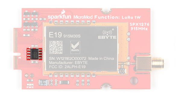
EEPROM
There is an I2C serial EEPROM on the LoRa function board. It has been reserved for future use, but users have access to it. A jumper is available on the back of the board to write protect the EEPROM (see the Jumpers section below).
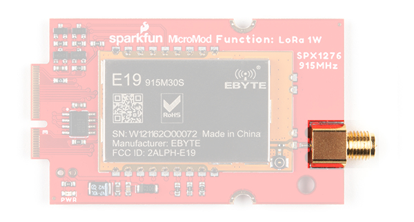
RP-SMA Antenna Connector
The LoRa function board features a sturdy RP-SMA antenna connector for users to attach an antenna of their choice. While this antenna connector is fairly robust, users should not expect to leverage a lot of weight off of it.
The edge-type antenna connector allows for the threads to protrude just beyond the edge of the board. Along with the dimensions of the LoRa function board, this feature is designed so that the connection also extends past the edge of the main board that the function board interfaces with; and is therefore, well suited to be used with an enclosure.
Note: Users who wish to use the u.FL connector can modify the position of this 0Ω resistor. Due to the size and position of the resistor, we only recommended for highly experience soldering experts attempt this modification. More novice users could potentially damage their LoRa function board if they attempt this modification.
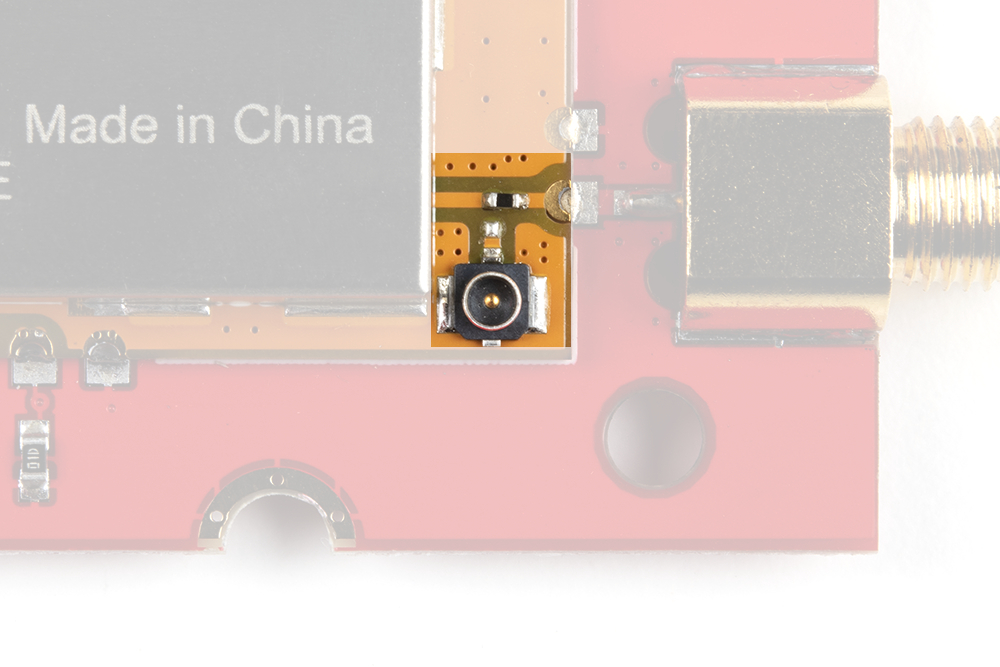
Antenna select jumper on the E19-915M30S RF transceiver module. (Click to enlarge)
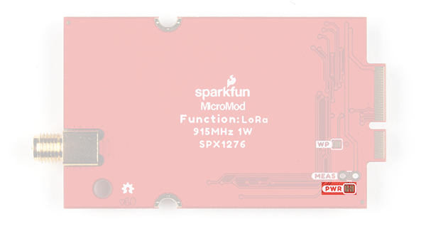
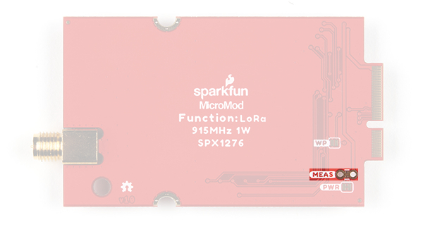
Jumpers
There are three jumpers available on the LoRa function board.
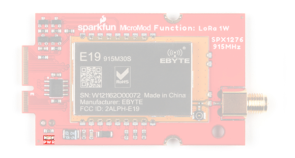
LED Power
For more low power projects, the PWR jumper can be cut to remove power from the red power LED.
Current Measurement
For users who would like to measure the current going to LoRa function board, the MEAS jumper can be cut and used for measurements. This jumper is only connected to the 5V power, which is used by only the E19-915M30S RF transceiver module and power LED.
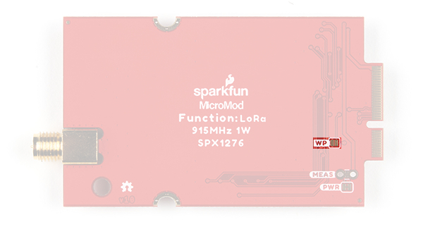
EEPROM Write Protection
To permanently write protect the EEPROM on the LoRa function board, users can bridge the WP jumper.