Using EAGLE: Board Layout
 jimblom
Layers Overview
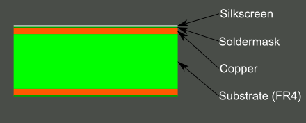
PCB composition is all about layering one material over another. The thickest, middle part of the board is a insulating substrate (usually FR4). On either side of that is a thin layer of copper, where our electric signals pass through. To insulate and protect the copper layers, we cover them with a thin layer of lacquer-like soldermask, which is what gives the PCB color (green, red, blue, etc.). Finally, to top it all off, we add a layer of ink-like silkscreen, which can add text and logos to the PCB.
EAGLE's Layers
The EAGLE board designer has layers just like an actual PCB, and they overlap too. We use a palette of colors to represent the different layers. Here are the layers you'll be working with in the board designer:
| Color | Layer Name | Layer Number | Layer Purpose |
|---|---|---|---|
| Top | 1 | Top layer of copper | |
| Bottom | 16 | Bottom layer of copper | |
| Pads | 17 | Through-hole pads. Any part of the green circle is exposed copper on both top and bottom sides of the board. | |
| Vias | 18 | Vias. Smaller copper-filled drill holes used to route a signal from top to bottom side. These are usually covered over by soldermask. Also indicates copper on both layers. | |
| Unrouted | 19 | Airwires. Rubber-band-like lines that show which pads need to be connected. | |
| Dimension | 20 | Outline of the board. | |
| tPlace | 21 | Silkscreen printed on the top side of the board. | |
| bPlace | 22 | Silkscreen printed on the bottom side of the board. | |
| tOrigins | 23 | Top origins, which you click to move and manipulate an individual part. | |
| bOrigins | 24 | Origins for parts on the bottom side of the board. | |
| / / Hatch | tStop | 29 | Top stopmask. These define where soldermask should not be applied. |
| \ \ Hatch | bStop | 30 | Absent soldermask on the bottom side of the board. |
| Holes | 45 | Non-conducting (not a via or pad) holes. These are usually drill holes for stand-offs or for special part requirements. | |
| tDocu | 51 | Top documentation layer. Just for reference. This might show the outline of a part, or other useful information. |
To turn any layer off or on, click the "Layer Settings..." button --  -- and then click a layer's number to select or de-select it. Before you start routing, make sure the layers above (aside from tStop and bStop) are visible.
Selecting From Overlapping Objects
Here's one last tip before we get to laying our board out. This is an interface trick that trips a lot of people up. Since the board view is entirely two-dimensional, and different layers are bound to overlap, sometimes you have to do some finagling to select an object when there are others on top of it.
Normally, you use the mouse's left-click to select an object (whether it's a trace, via, part, etc.), but when there are two parts overlapping exactly where you're clicking, EAGLE doesn't know which one you want to pick up. In cases like that, EAGLE will pick one of the two overlapping objects, and ask if that's the one you want. If it is, you have to left-click again to confirm. If you were trying to grab one of the other overlapping objects, right-click to cycle to the next part. EAGLE's status box, in the very bottom-left of the window, provides some helpful information when you're trying to select a part.
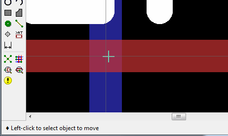
For example: In the GIF above, a VCC net overlaps another named Reset. We left-click once directly where they overlap, and EAGLE asks us if we meant to select VCC. We right-click to cycle, and it asks us instead if we'd like to select Reset. Right-clicking again cycles back to VCC, and a final left-click selects that as the net we want to move.
Whew! Enough pointers, let's lay out a PCB!