Using EAGLE: Board Layout
Finishing Touches
Adding Copper Pours
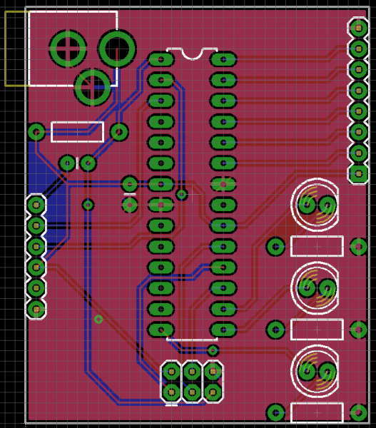
Copper pours are usually a great addition to a board. They look professional and they actually have a good reason for existing. Not to mention they make routing much easier. Usually, when you're adding a copper pour it's for the ground signal. So let's add some ground pours to the design.
Start by selecting the POLYGON tool --  . Then (as usual), you'll need to adjust some settings in the options bar. Select the top copper (1) layer. Also adjust the Isolate setting which defines how much clearance the ground pour gives other signals, 0.012" for this is usually good.
Next, draw a set of lines just like you did the dimension box. In fact, just draw right on top of the dimension lines. Start drawing at the origin, trace all the way around, and finish back at the same spot. A dotted red box should appear around the dimension of the board.
After you've drawn the polygon, you have to connect it to a net using the NAME tool --  . This works just like naming nets on a schematic. Use that tool on the dotted red line you just created, and in the dialog that pops up type "GND". (Click here to see an animated GIF of the entire process.)
The last step is to hit ratsnest, to watch the glorious red pour fill just about the entire area of your board. You'll probably hate me for telling you this now, but adding ground pours to your design at the very beginning (after placing parts, before routing) makes manual routing much easier.
You can (and probably should) have ground pours on both sides of the board, so follow the same set of steps on the bottom layer.
It can be hard to tell what is and isn't connected to the ground pour. If you see a black gap separating a pad and the pour, there is no connection. If you see some traces forming a "target" over the pad, there is a connection from the pour to that pad.
If you ever want to hide the polygon (it's hard to see other stuff with it on there), use the RIPUP tool on the polygon border you just drew. Don't worry, the polygon is still there, just hit ratsnest to bring it back.
Adding Silkscreen
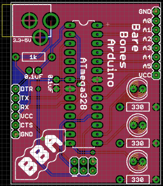
Although it has no real effect on the circuit your designing, silkscreen can be a critical part of the PCB design. You want it to look good, right? Some silkscreen -- like part outlines -- is automatically placed on the board because it's a piece of the part. We can manually add other information, like labels, logos, and names. A variety of draw tools -- wire ( ), text (
 ), circle (
 ), arc (
 ), rectangle (
 ), and polygon (
 ) -- can be used to draw on the silkscreen layer (tPlace for top, bPlace for bottom).
Have fun and explore with these tools. You could add labels for the headers, or values for the resistors, or even create a nifty logo.
The draw tools are a bit limited, but that doesn't mean you can't make it look good!


