smôl Hookup Guide
 PaulZC
FPC Connections
We love Flexible Printed Circuit (FPC) connections and we're using them in more and more of our products.
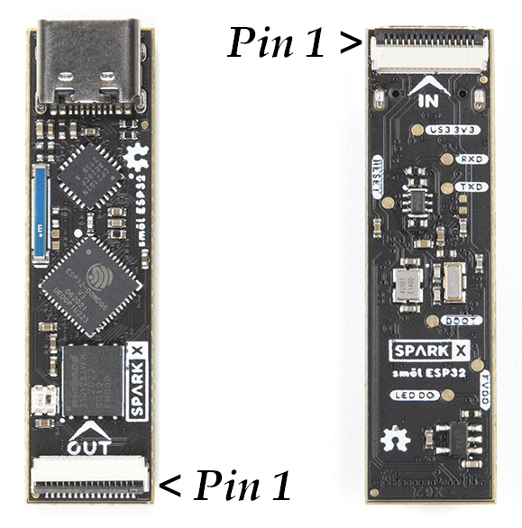
Each smôl board (except the Header) comes with two 16-way FPC connectors, labelled IN and OUT. The IN connector is on the bottom of each board, the OUT is on top. Matching FPCs connect the OUT connector on one board to the IN connector on the next.
Our 36mm FPC is the perfect length if you want the smôl boards to stack neatly, one on top of the other. The connectors have "dual contacts" (contacts top and bottom) and so it does not matter which way round you insert the FPC, it will always make contact.
We wanted the smôl boards to be as small as possible and so we've put a lot of thought into the signals on those 16 FPC connections to make them as efficient as possible. The standard pin-out of the connector is as follows:
| Connector Pin No. | Signal Name | Function |
|---|---|---|
| 1 | PROC_PWR_EN | Processor Power Enable |
| 2 | 3V3 | 3.3V Power Rail |
| 3 | GND | Power Ground / 0V |
| 4 | SCLK | SPI Clock |
| 5 | COPI | SPI Controller Out Peripheral In |
| 6 | CIPO | SPI Controller In Peripheral Out |
| 7 | CS0 | SPI Chip Select 0 |
| 8 | CS1 | SPI Chip Select 1 |
| 8 | CS2 | SPI Chip Select 2 |
| 10 | GPIO0 | General Purpose Input / Output 0 |
| 11 | GPIO1 | General Purpose Input / Output 1 |
| 12 | SDA | I2C Data |
| 13 | SCL | I2C Clock |
| 14 | GND | Power Ground / 0V |
| 15 | 3V3 | 3.3V Power Rail |
| 16 | V_USB | USB Power Rail (5V) |
On our Eagle schematics, the connections usually look like this:
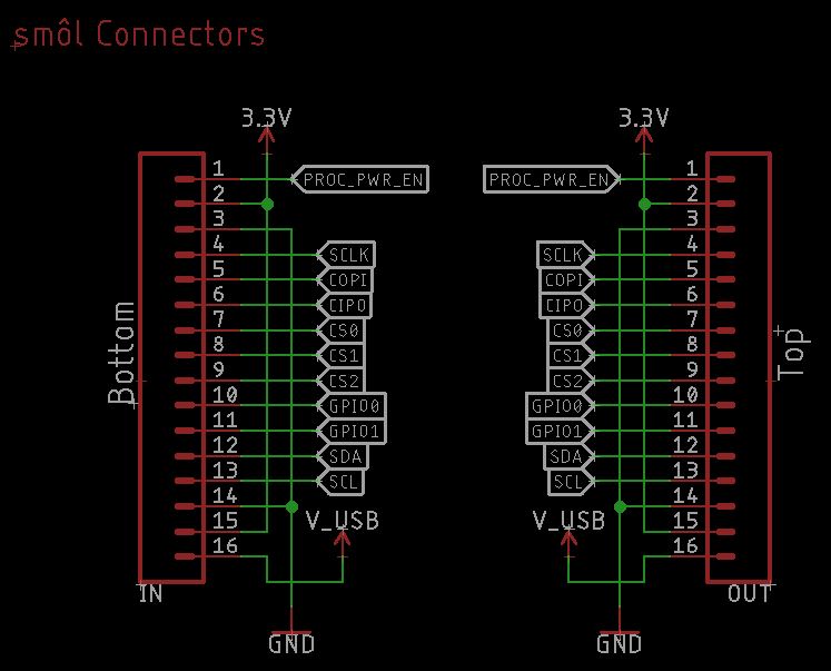
We say "usually" because the exact connections depend on the board type. More about that in a moment.
First, let's talk about what each pin does:
Pin 1: PROC_PWR_EN
Processor Power Enable is a signal which is passed up and down the smôl stack. It is connected to the enable pin of the 3.3V voltage regulator on the processor board. If PROC_PWR_EN is pulled high, or is left floating, the processor board voltage regulator will be enabled and will generate 3.3V from USB-C.
When you connect a Power Board to your smôl stack, PROC_PWR_EN allows the power board to disable the regulator on the processor board. The power board is then responsible for generating the 3.3V power rail for the entire smôl stack. We do this for two reasons: to prevent the power board and processor board regulators from fighting each other; and to allow the power board to power down the entire smôl stack even if USB is connected.
One of the clever features of smôl is that the power boards can be instructed to power down the whole stack for a pre-defined duration. Power down durations of a few 10's of milliseconds to several days are possible. During power down the only device left running is the ATtiny processor on the power board, which typically consumes less than 10 microamps. PROC_PWR_EN allows smôl to avoid the quiescent current normally drawn by the processor regulator.
Pins 2 and 15: 3.3V Power
Pins 2 and 15 carry 3.3V power up and down the smôl stack. 3.3V can be generated by a processor board, powered by USB-C. Or, 3.3V power can be generated by one of our power boards.
As described above, the power board can disable the regulator on the processor board via the PROC_PWR_EN pin, avoiding the associated quiescent current draw.
Pins 3 and 14: GND
Pins 3 and 14 are the smôl Power Ground or 0V pins.
You will note that the highest speed smôl signals (SPI SCLK and I2C SCL) are run adjacent to the GND connections to minimize EMI.
Pins 4-6: SPI SCLK, COPI and CIPO
Pins 4-6 carry the clock and data signals for the Serial Peripheral Interface (SPI).
The Processor Board is the SPI Controller and can communicate with smôl Peripheral boards at high data rates.
SPI devices share common clock and data signals but require an individual Chip Select signal. The smôl Chip Select signals are described in the next paragraph.
Pins 7-9: SPI CS0, CS1 and CS2
Pins 7-9 are the smôl SPI Chip Select signals and allow up to three SPI Peripheral Boards to be connected into your smôl stack.
We use a technique called waterfalling when linking the chip select lines from one smôl board to the next. There is a full description of this in the SPI Chip Select Waterfalling section of this guide.
If your favorite 3.3V SPI breakout board is not yet available in smôl format, you can connect it via the breakout pins on the smôl Header.
Pins 10 and 11: GPIO0 and GPIO1
Pins 10 and 11 carry two General Purpose Input / Output signals: GPIO0 and GPIO1. These are typically used as power control signals to power down individual Peripheral Boards, again to allow the current draw to be minimized as much as possible.
Just like the SPI Chip Select signals, GPIO0 and GPIO1 are also waterfalled. If a Peripheral Board uses GPIO0, then GPIO1 is waterfalled onto GPIO0 of the board's OUT connector. Please see the full description of this in the GPIO Waterfalling section of this guide.
Pins 12 and 13: I2C SDA and SCL
Pins 12 and 13 carry the data and clock signals for Inter-Integrated Circuit (I2C) communication.
Multiple I2C boards can be connected to smôl provided each has a unique address.
If your favorite Qwiic board is not yet available in smôl format, you can connect it via the Qwiic connector on the smôl Header.
Pin 16: V_USB
Pin 16 carries 5V power from the USB-C connector on the Processor Board up and down the smôl stack.
V_USB is used by the smôl Power Board LiPo to recharge the LiPo battery when USB-C is connected. We limited the charge current to 100mA to avoid drawing too much current through the single V_USB FPC trace.
Pin Numbering
Just to clarify which is pin 1:
When viewed from the front or top of the board, pin 1 of the OUT connector is on the right.
When the board is turned over, pin 1 of the IN connector is on the left.