RP2040 mikroBUS™ Development Board Hookup Guide
This Tutorial is Retired!
This tutorial covers concepts or technologies that are no longer current. It's still here for you to read and enjoy, but may not be as useful as our newest tutorials.
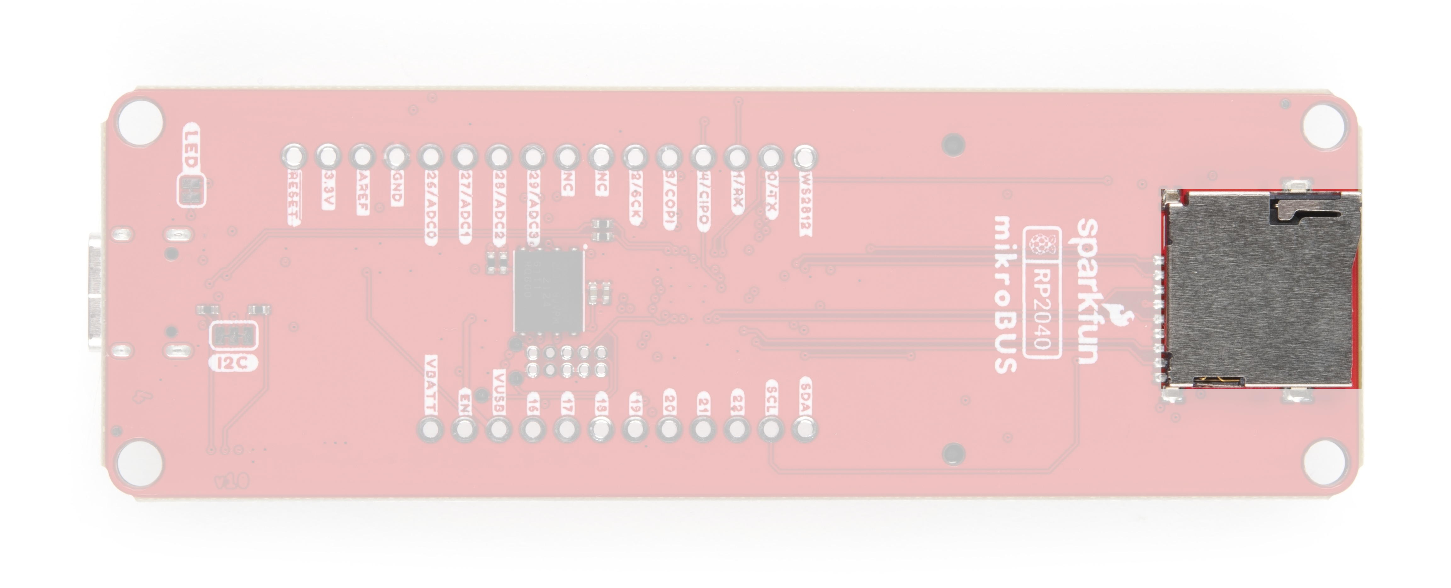
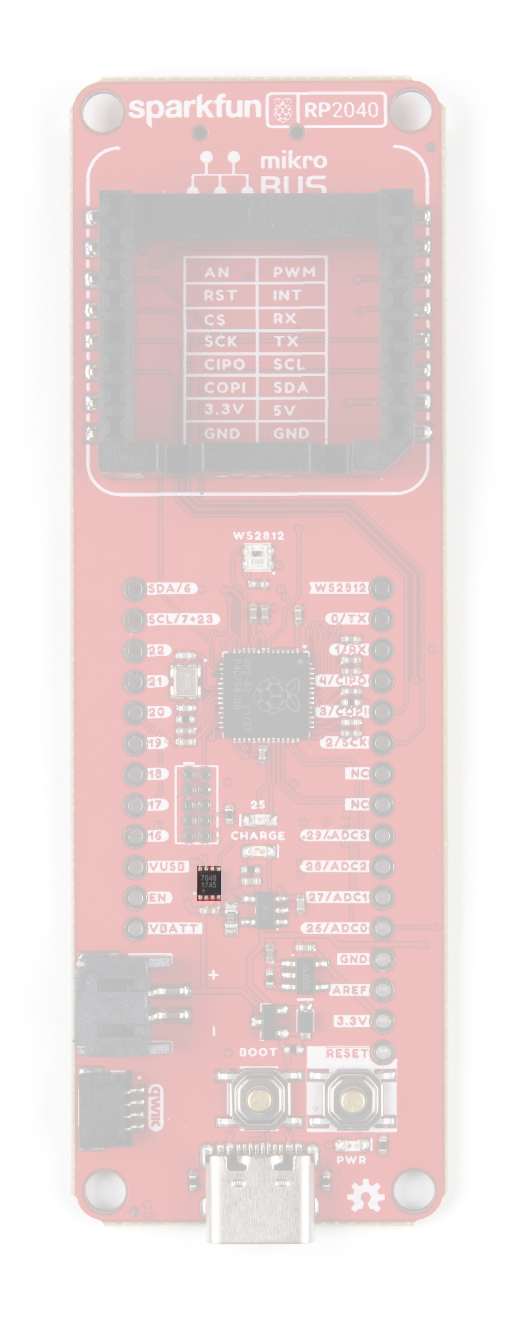
Hardware Overview
Note: Users may notice similarities between the RP2040 Thing Plus and the RP2040 mikroBUS™ development board. These boards are nearly identical, apart from the board dimensions and the mikroBUS™ socket. Please refer to the RP2040 Thing Plus hookup guide for more details on the board design.
RP2040 Thing Plus Hookup Guide
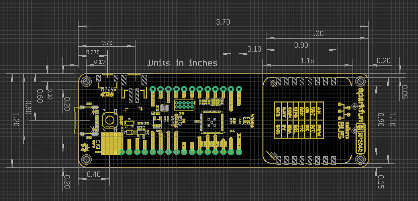
Board Dimensions
The RP2040 mikroBUS™ Development Board's pin layout has a feather form factor with a mikroBUS™ socket above. The board dimensions are illustrated in the drawing below.
Power
The RP2040 mikroBUS™ Development Board only requires 3.3V to power the board. However, the simplest method to power the board is through the USB-C connector.
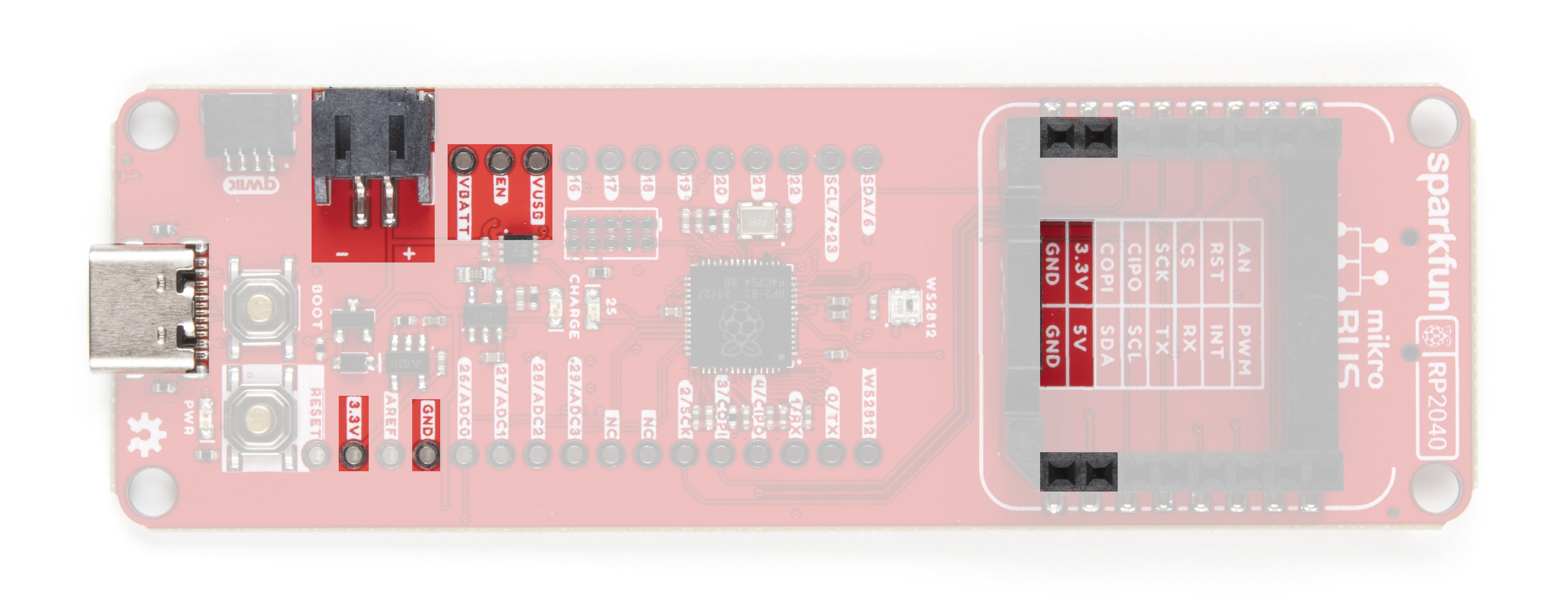
The power pins that are available on the board, are detailed below:
3V3- A regulated 3.3V voltage source (600mA).- Regulated from the USB 5V power and/or battery connection by a AP2112 LDO.
- Used to power the RP2040 MCU, WS2812 RGB LED, W25Q128 16MB flash chip, µSD card slot,
+3.3Vpin of the mikroBUS™ socket, and the Qwiic bus (I2C). - Serves as the reference voltage for the RP2040 ADC (
ADC_VDD). - Pin can also operate as an input from an external power source.
USB- The voltage from the USB-C connector, usually 5V.- Used to provide a regulated 3.3V source through the AP2112 LDO (see above).
- Serves as the power supply for the MCP73831 linear charge management controller to the JST battery connector.
- Serves as the power supply for the
+5Vpin of the mikroBUS™ socket. - Utilizes a P-channel MOSFET to control the power source for the AP2112 LDO.
- Utilizes a BAT20J protection diode for the USB-C connection.
VBAT- The voltage from the JST battery connector; meant for single cell LiPo batteries.- Used to provide a regulated 3.3V source through the AP2112 LDO (see above).
- Connected to the MCP73831 linear charge management controller.
GND- The common ground or the 0V reference for the voltage supplies.
Note: The RP2040 microcontroller has two low power states:
SLEEP- All the processors are asleep and most of the clocks in the chip are stoppedDORMANT- All clocks in the chip are stopped
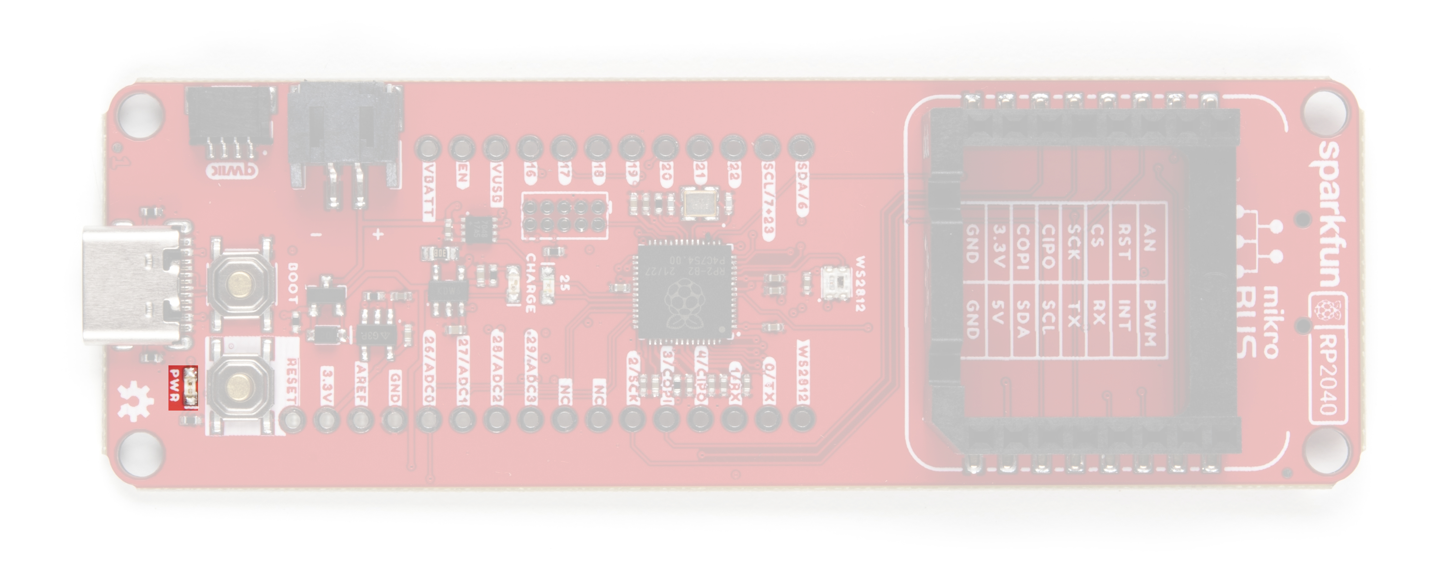
Power Status LED
The red, POWER LED will light up once 3.3V is supplied to the board; however, for most users, it will light up when 5V is supplied through the USB connection or when a LiPo battery is connected to the JST connector.
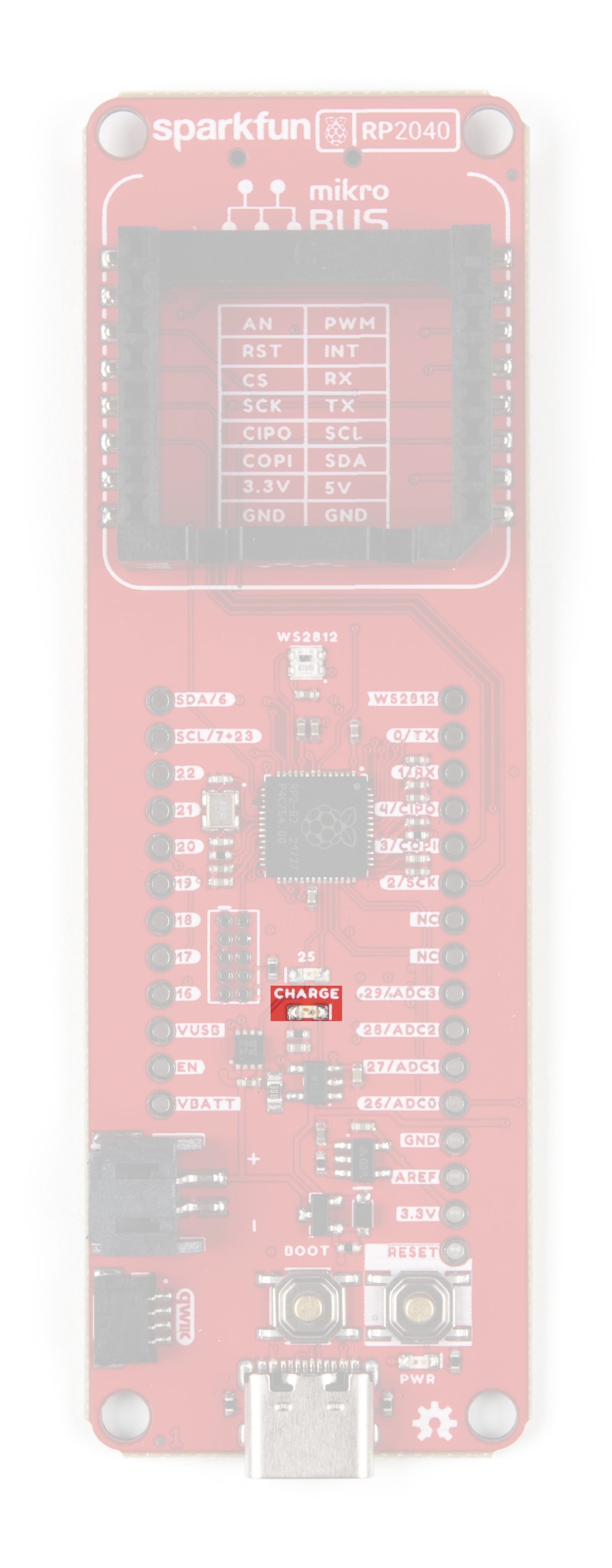
POWER status LED indicator. (Click to enlarge) Charging Circuit
The charging circuit utilizes the MCP73831 linear charge management controller and is powered directly from the USB-C connector or USB. The controller is configured for a 500mA charge rate and battery charging is indicated when the yellow, CHG LED. If the charge controller is shutdown or charging is complete, the CHG LED will turn off. For more information, pleas refer to the MCP73831 datasheet.
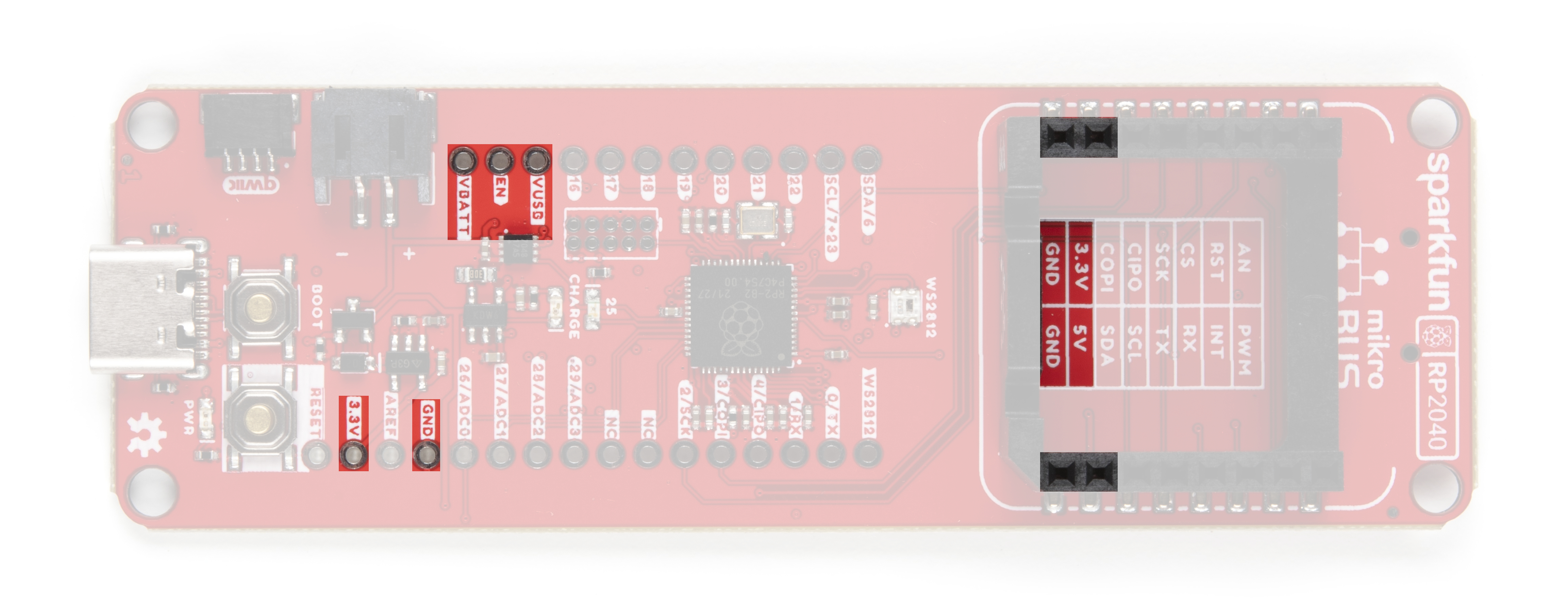
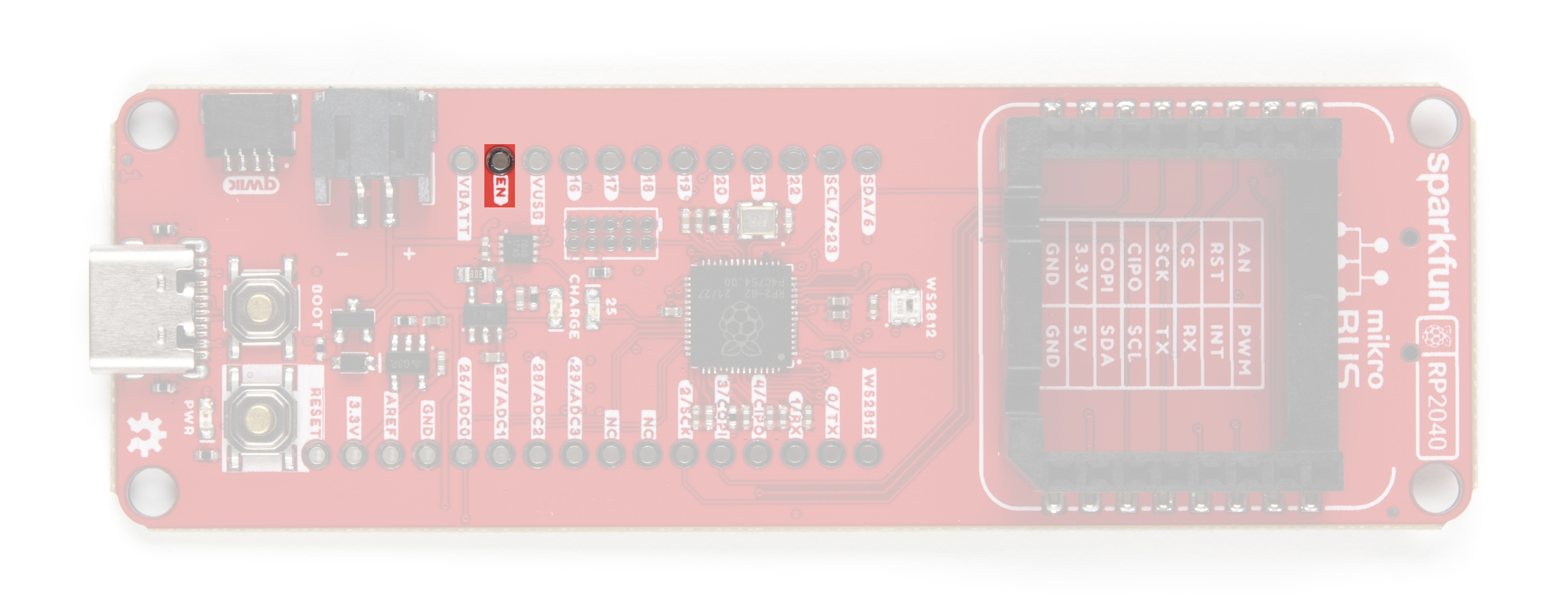
Power Control
The power source to the AP2112 LDO voltage regulator is controlled by a P-channel MOSFET. In addition, the 3.3V regulated output from the AP2112 is controlled by the enable (EN) pin, broken out on the board. By default, the chip enable pin (EN) is pulled high, to enable the 3.3V output, supply voltage. To disable and shutdown the output voltage from the AP2112, the chip enable pin (EN) needs to be pulled low (i.e. shorted to ground (GND)). For more information, pleas refer to the AP2112 datasheet.
RP2040 Microcontroller
The Raspberry Pi RP2040 is a low-cost, high-performance microcontroller with flexible digital interfaces. It features:
- Dual Arm® Cortex®-M0+ processors, up to 133 MHz
- 264 kB of embedded SRAM in 6 banks
- 6 dedicated IO for additional storage
- Connects to QSPI Flash
- Supports execute in place (XIP))
- 30x 3.3V user-programmable high-speed IO (only 18 are broken out on the board)
- 4x 12-bit 500ksps Analogue to Digital Converter (ADC)
- Various digital peripherals
- 2x UART, 2x I2C, 2x SPI, up to 16 PWM channels
- 1x Timer with 4 alarms, 1x Real Time Counter
- USB 1.1 Host/Device compatible
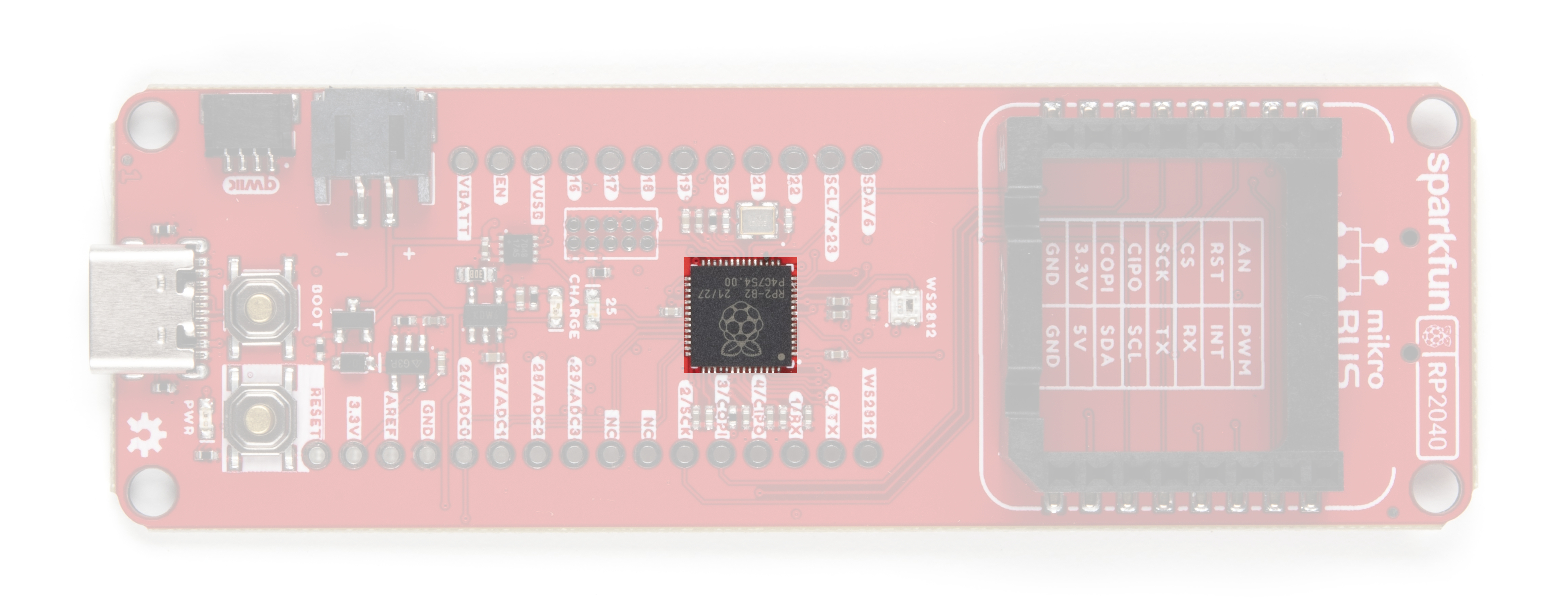
The processor implements the ARMv6-M Thumb instruction set and provides programmable (multifunction) IO (PIO), which is unique to the RP2040. For more information, pleas refer to the RP2040 datasheet.
USB Functionality
The RP2040 contains a USB 2.0 controller that can operate as either:
- Full Speed device (12 Mbit/s)
- Host that can communicate with both Low Speed (1.5 Mbit/s) and Full Speed devices. This includes multiple downstream devices connected to a USB hub.
USB Mass Storage Interface
The Bootrom provides a standard USB bootloader that emulates a writeable drive available for loading firmware to the RP2040
using UF2 files. Once a UF2 file is loaded onto the drive, it is written to the flash or RAM and the device automatically reboots.
- The bootrom source code is hosted on GitHub.
RPI-RP2 Drive
The RP2040 appears as a standard 128MB flash drive named RPI-RP2 formatted as a single partition with FAT16. There
are only ever two actual files visible on the drive specified.
INFO_UF2.TXT- contains a string description of the UF2 bootloader and version.INDEX.HTM- redirects to information about the RP2040 device.
.uf2 file is written to the device however, the special contents are recognized and data is written to specified locations in RAM or Flash. On the completed download of an entire valid .uf2 file, the RP2040 automatically reboots to run the newly downloaded code.Flash Memory
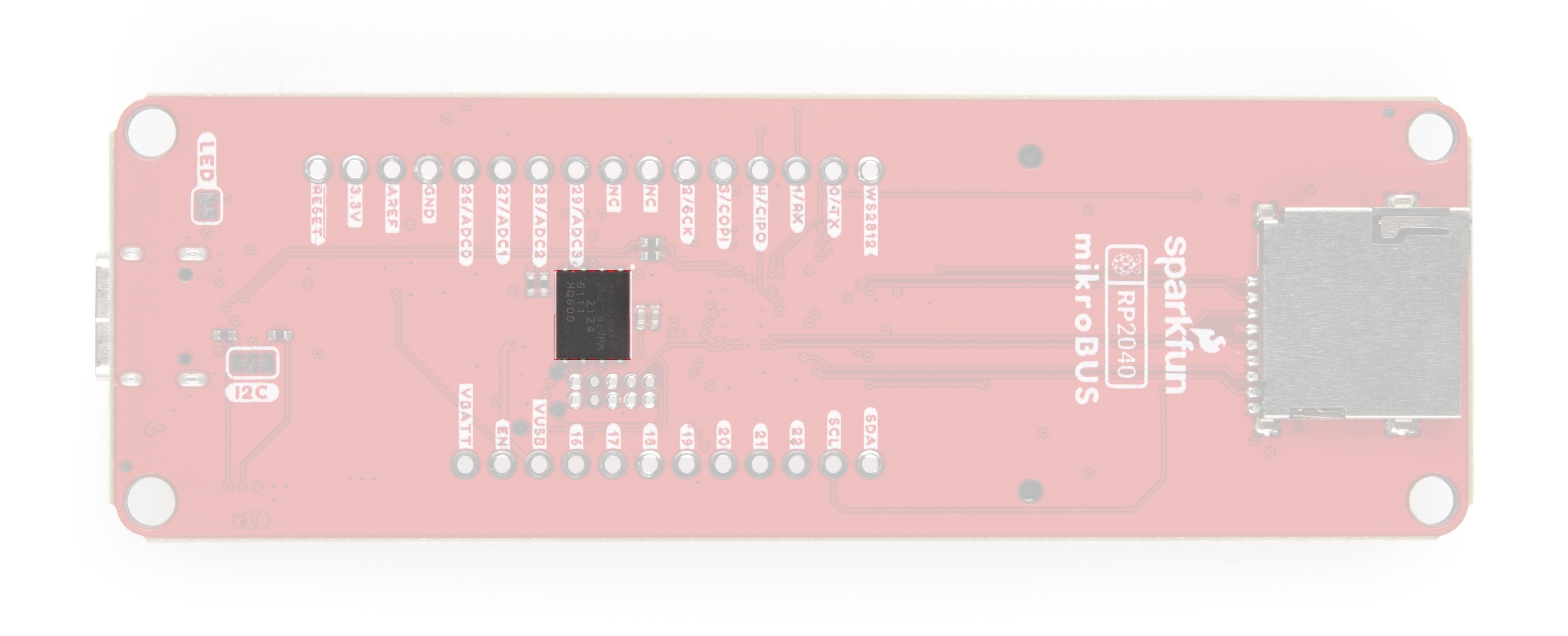
RP2040 has embedded ROM and SRAM, and access to external flash via a QSPI interface. On the RP2040 mikroBUS™ development board, an additional 16MB (128Mbit) of 133MHz memory is provided by a W25Q128JVPIM chip. The flash memory is required for the RP2040 to store program code, which it can boot and run from through its dedicated QSPI pins:
- Pin 52:
CLK - Pin 56:
CS - Pin 53:
DATA 0/DI - Pin 55:
DATA 1/DO - Pin 54:
DATA 2/WP - Pin 51:
DATA 3/HOLD
0x10000000.Indicator LEDs
There are 4 indication LEDs on the RP2040 mikroBUS™ development board for:
PWR: Power (Red)CHG: Battery Charging (Yellow)25:GPIO 25(Blue)WS2812:GPIO 08(RGB)
Power LED
The red, PWR LED will light up once 3.3V is supplied to the board. For most users, it will light up when 5V is supplied through the USB connection and/or when a LiPo battery is attached to the JST connector.
PWR status LED indicator. (Click to enlarge) Battery Charging LED
The yellow, CHG LED will light while a battery is being charged through the charging circuit. The LED will be off when no battery is present (*or dimmed), when the charge management controller is in standby (after the battery charging has been completed), or when the charge management controller is shutdown (thermal shutdown or when the input voltage is lower than the battery voltage). The LED will be on when the charge management controller is in the process of charging the battery. For more information, please refer to the MCP73831 datasheet.
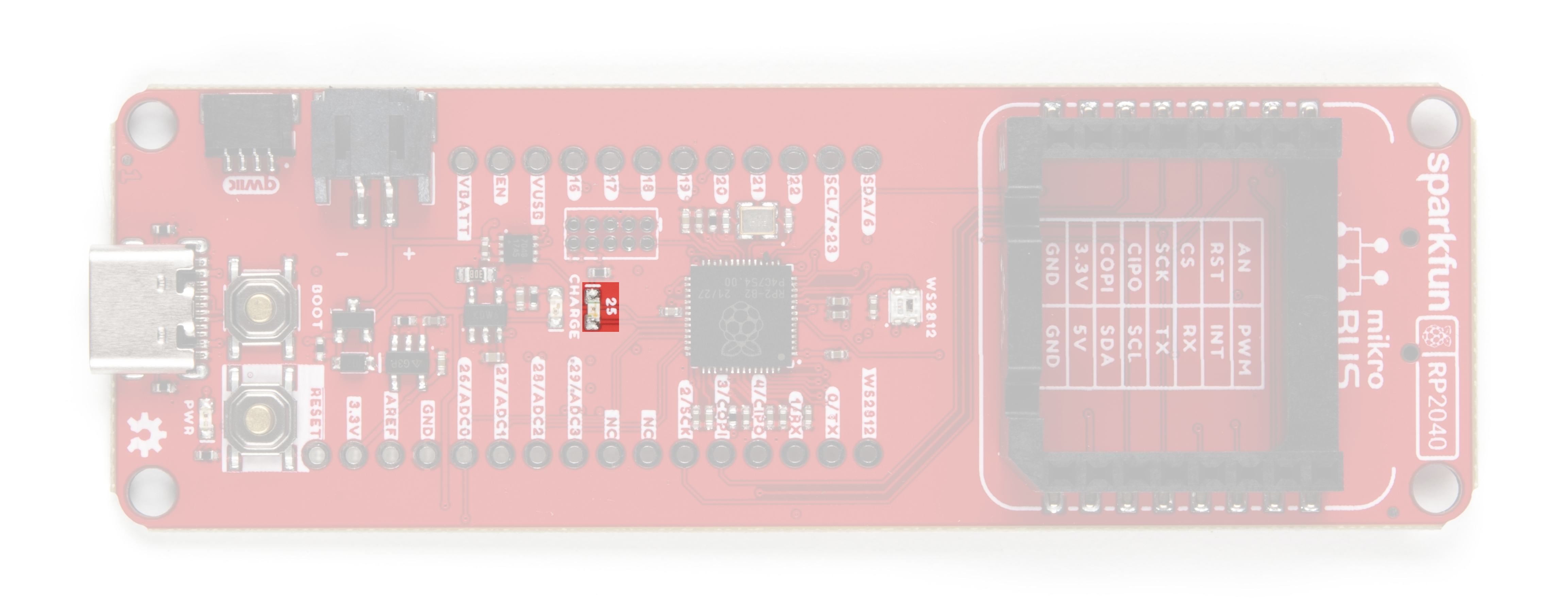
The battery charging (
CHG) LED indicator on the RP2040 mikroBUS™ development board. (Click to enlarge)
| Charge Cycle State | STAT1 |
|---|---|
Shutdown
|
Off (High Z) |
| No Battery Present* | Dimmed (High Z) |
| Charge Complete – Standby | Off (H) |
| Preconditioning | On (L) |
| Constant-Current Fast Charge | On (L) |
| Constant Voltage | On (L) |
*The charge LED may appear dimmed due a trickle charge from the MAX17048 fuel gauge. Normally, the LED should be OFF.
Status LED
The blue, 25 LED is typically used as a test or status LED to make sure that a board is working or for basic debugging. This indicator is connected to GPIO 25.
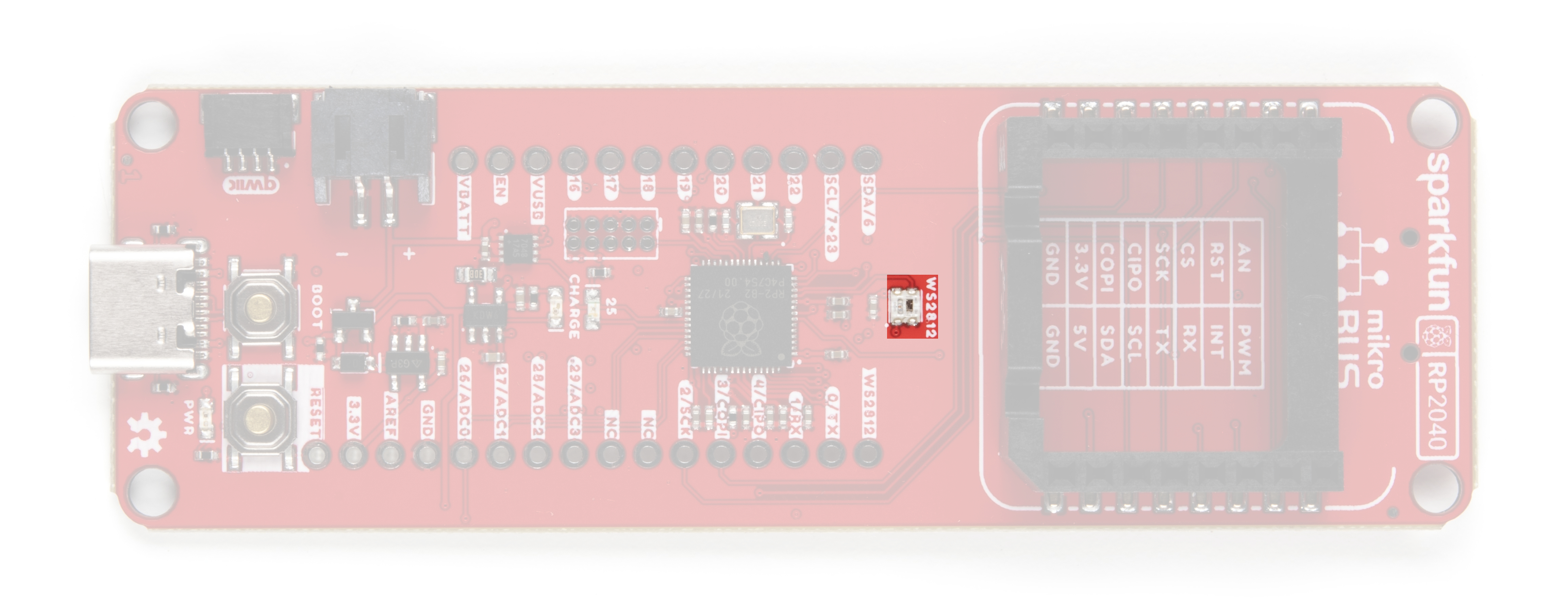
25) LED indicator on the RP2040 mikroBUS™ development board. (Click to enlarge) WS2812 RGB LED
The WS2812 RGB LED is controlled with a 24-bit (GRB) data signal. This indicator is connected to GPIO 08 and the digital output pin from the LED is broken out as the WS2812 pin on the board. For more information, please refer to the WS2812C datasheet.
WS2812 LED indicator on the RP2040 mikroBUS™ development board. (Click to enlarge) Buttons
The RP2040 mikroBUS™ dev. board has two buttons on the board for uploading and running code.
Reset Button
The RESET button is connected to the reset pin and is used to reset the microcontroller without needing to unplug the board.
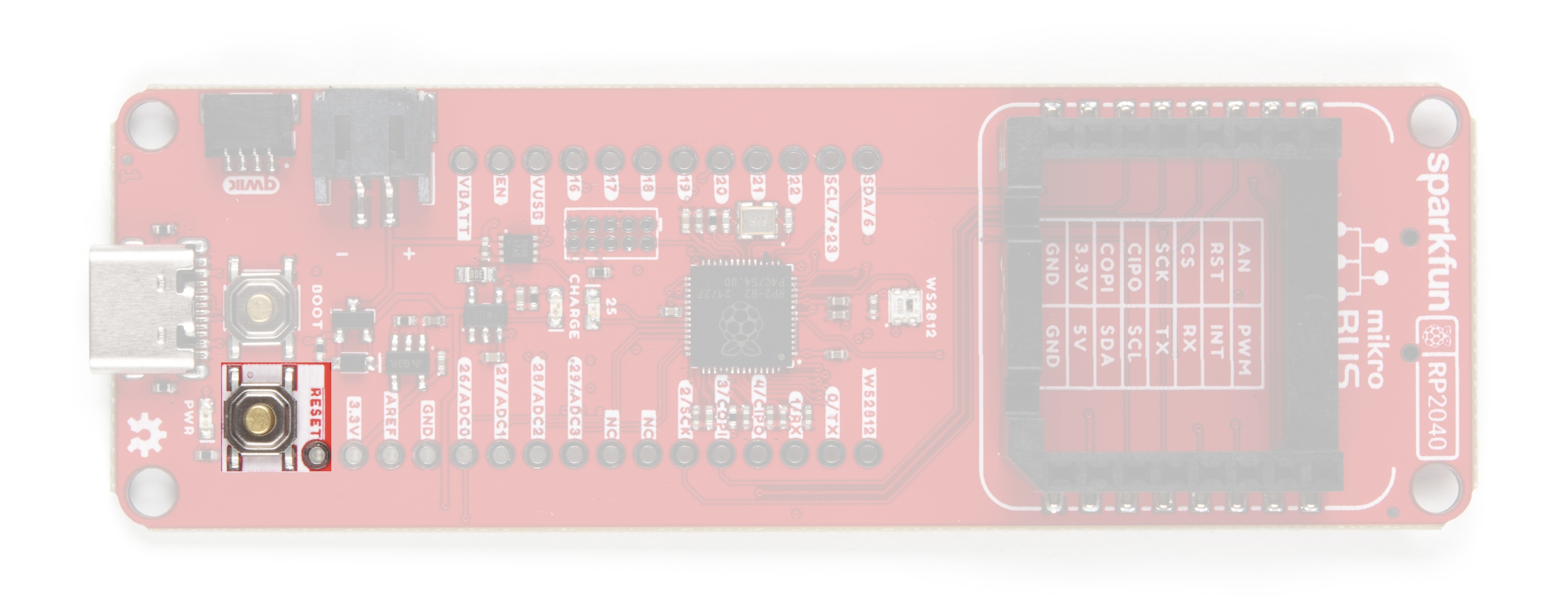
RESET button on the RP2040 mikroBUS™ development board. (Click to enlarge) Boot Button
The BOOT button is used to force the board into BOOTSEL mode, by holding down the BOOT button while connecting the board to a computer through its USB-C connector. Users can then, upload firmware files to the emulated RPI-RP2 USB mass storage device.
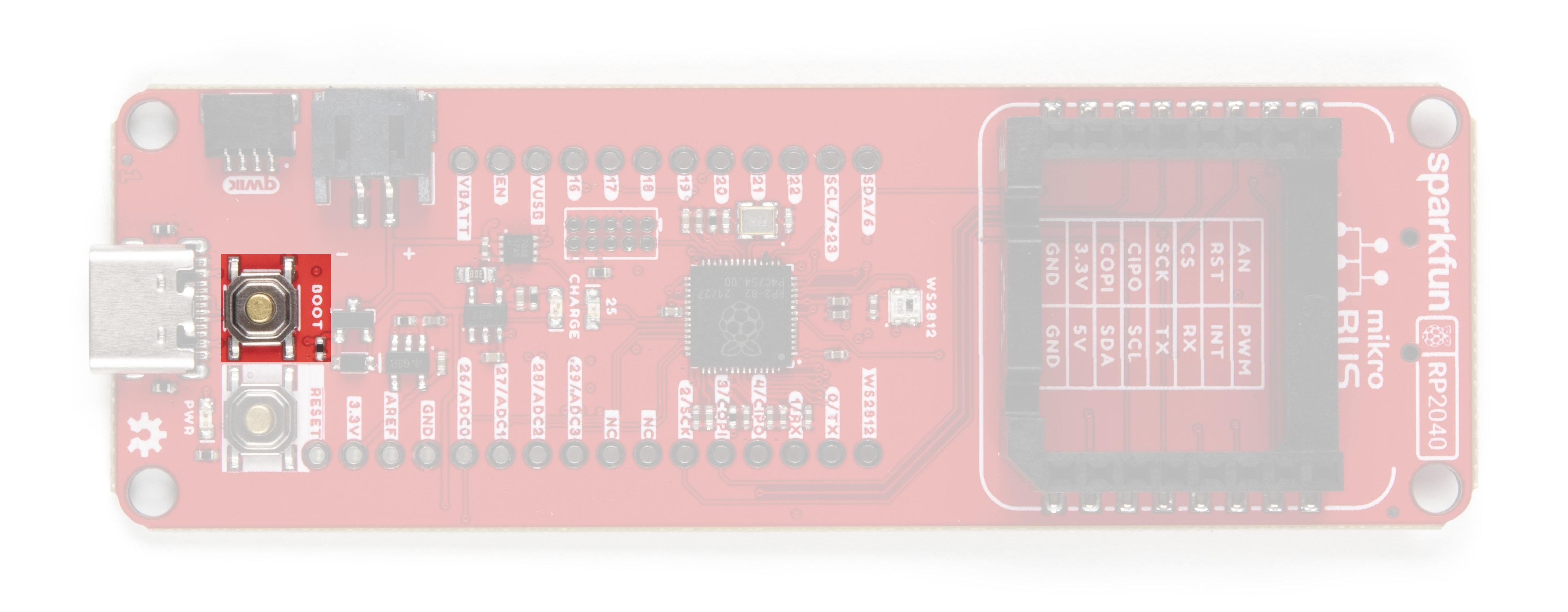
BOOT button on the RP2040 mikroBUS™ development board. (Click to enlarge) BOOTSEL Mode: Users can enter BOOTSEL mode by holding down the BOOT button, when the USB connection is made to a computer. The board will remain in this mode until it power cycles (happens automatically after uploading a .uf2 firmware file) or the RESET button is pressed. The board will appear as a USB mass storage device under the name RPI-RP2.
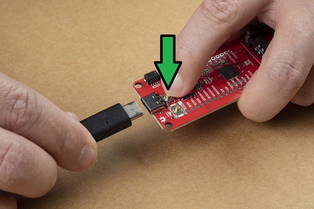
Hold down
BOOT button to enter BOOTSEL mode on The SparkFun Thing Plus - RP2040. (Click to enlarge)
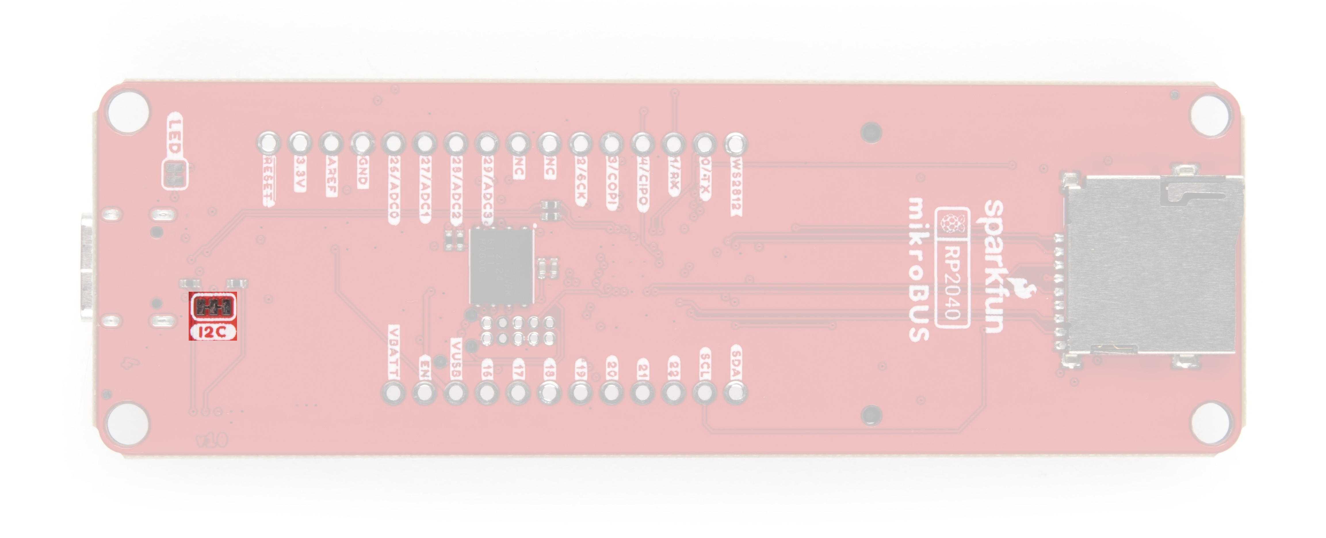
MikroBUS™ Socket
The most significant feature of this board, is the addition of the MikroBUS™ socket, which provides a drop-in interface for MikroElectronka&apo;s ecosystem of Click boards™ (over 1079 as of September 2021).
The mikroBUS™ socket comprises a pair of 8-pin female headers with a standardized pin configuration. The pins consists of three groups of communications pins (SPI, UART and I2C), six additional pins (PWM, Interrupt, Analog input, Reset and Chip select), and two power groups (3.3V and 5V).
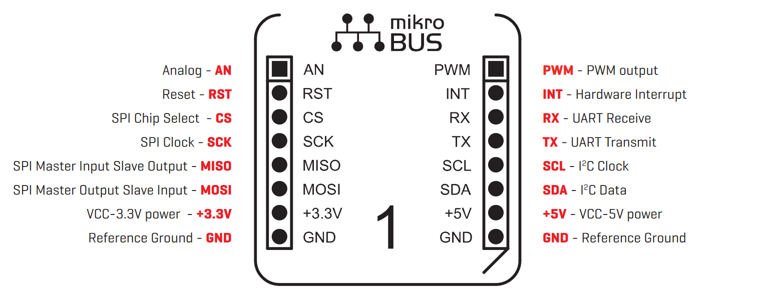
GPIO 02:SCKGPIO 03:MOSI(COPI)GPIO 04:MISO(CIPO)GPIO 05:CS
GPIO 06:SDAGPIO 07/23:SCL
GPIO 0:TXGPIO 01:RX
GPIO 13:RSTGPIO 16:PWMGPIO 17:INTGPIO 26:AN
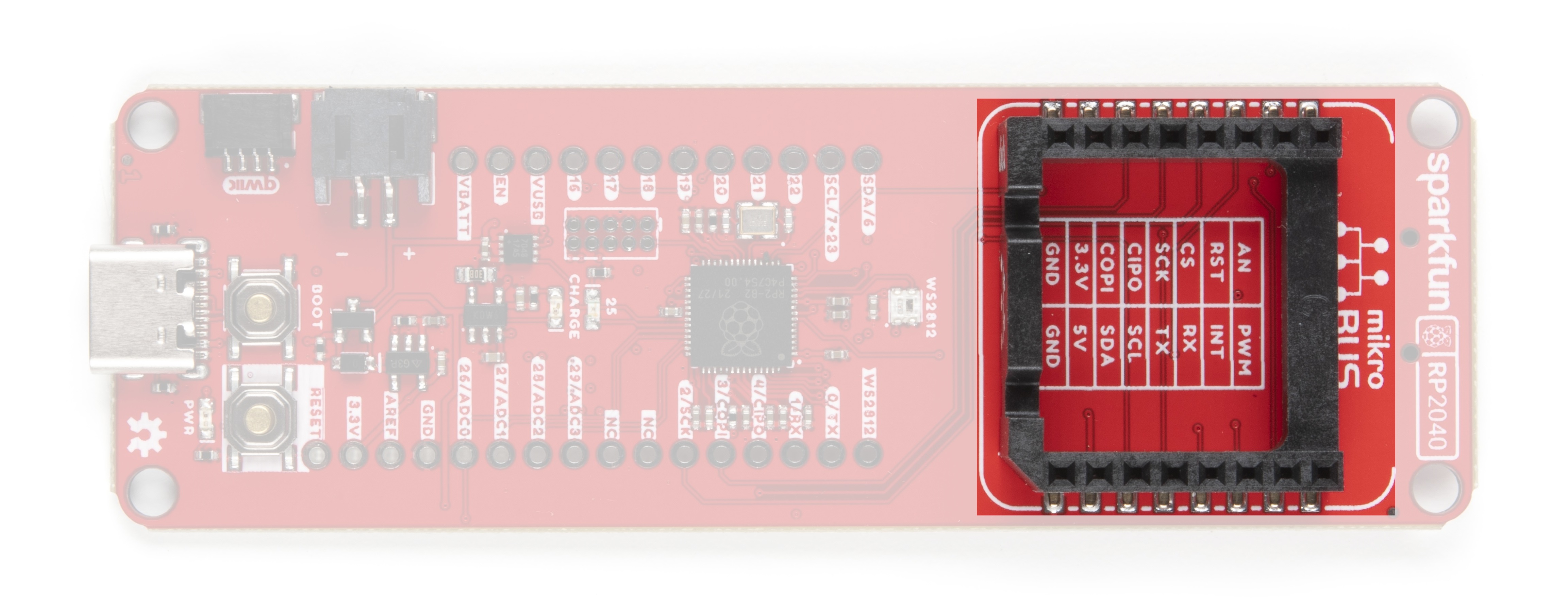
MikroBUS™ socket on the RP2040 mikroBUS™ development board. (Click to enlarge)
*For more information about the mikroBUS™ socket, click here for the mikroBUS™ standard specifications.
µSD Slot
MOSI signal on a controller has been replaced with the title SDO. Please refer to this announcement on the decision to deprecate the MOSI/MISO terminology and transition to the SDO/SDI naming convention.
The RP2040 mikroBUS™ development board includes an µSD card slot. This is great for data logging applications or storing files. The µSD card slot is connected to the following dedicated GPIO:
GPIO 09:DATA 3/CSGPIO 10:DATA 2GPIO 11:DATA 1GPIO 12:DATA 0/CIPO(or Peripheral'sSDO)GPIO 14:CLK/SCKGPIO 15:CMD/COPI(or Peripheral'sSDI)
Primary I2C Bus
A (battery) fuel gauge and a Qwiic connector are attached to the primary I2C bus I2C1. The primary I2C bus for this board utilizes the GPIO connections, detailed in the table below:
| Connection | VDD |
GND |
SCL |
SDA |
|---|---|---|---|---|
| Pin Number | 3.3V | GND |
Pin 9 Pin 35 |
Pin 8 |
| GPIO | 3.3V | GND |
GPIO 07GPIO 23
|
GPIO 06 |
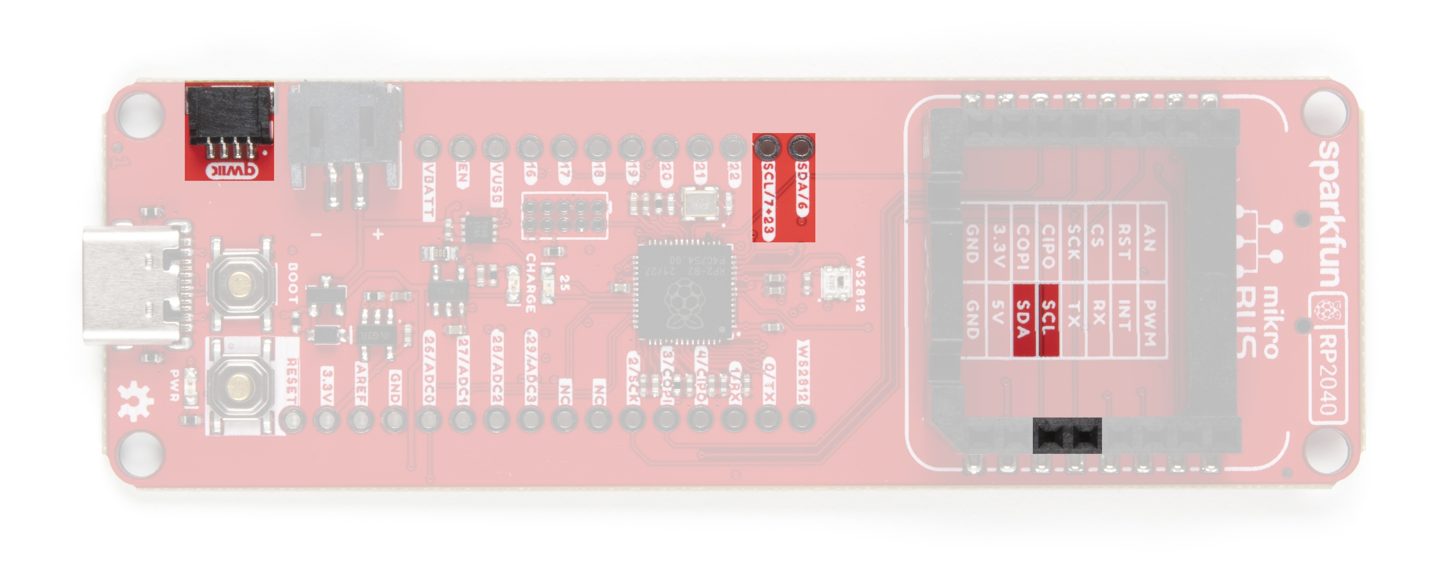
Note: The clock line of the I2C bus is tied between pins 9 and 35 (GPIO 07 and GPIO 23). This allows GPIO 16 - GPIO 23 to be aligned on the board's edge, for a consecutive, eight pin bus; useful for things like HDMI.
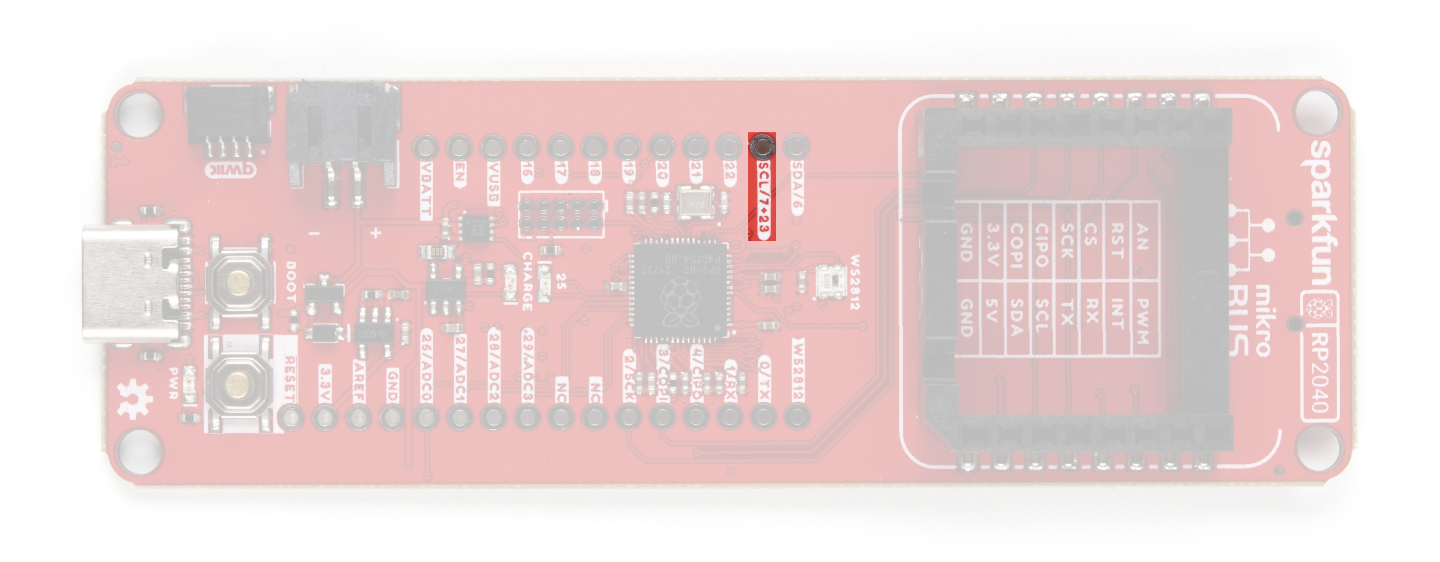
Shared pin for
GPIO 07 and GPIO 23 on the RP2040 mikroBUS™ development board. (Click to enlarge)
*Since the two GPIO pins are tied together, they cannot operate simultaneously.
Battery Fuel Gauge
The MAX17048 fuel gauge measures the approximate charge or discharge rate, state of charge (SOC) (based on ModelGauge algorithm), and voltage of a connected battery. Additionally, there is a configurable alert pin functionality for low SOC, 1% SOC, reset, overvoltage, or undervoltage. For more information, pleas refer to the MAX17048 datasheet.
The MAX17048 fuel gauge on the RP2040 mikroBUS™ development board. (Click to enlarge)
| I2C Address |
0x36 (7-bit) 0x6C (write)/0x6D (read) |
| Voltage Measurement |
Range: 2.5 - 5 V Precision: ±7.5 mV/Cell Resolution 1.25 mV/Cell |
| Current Consumption |
Sleep: .5 - 2 µA Hibernate: 3 - 5 µA Active: 23 - 40 µA |
| Alert Indicators: |
Low SOC 1% Change in SOC Battery Undervoltage/Overvoltage VRESET Alert |
| Alert Pin | GPIO 24 |
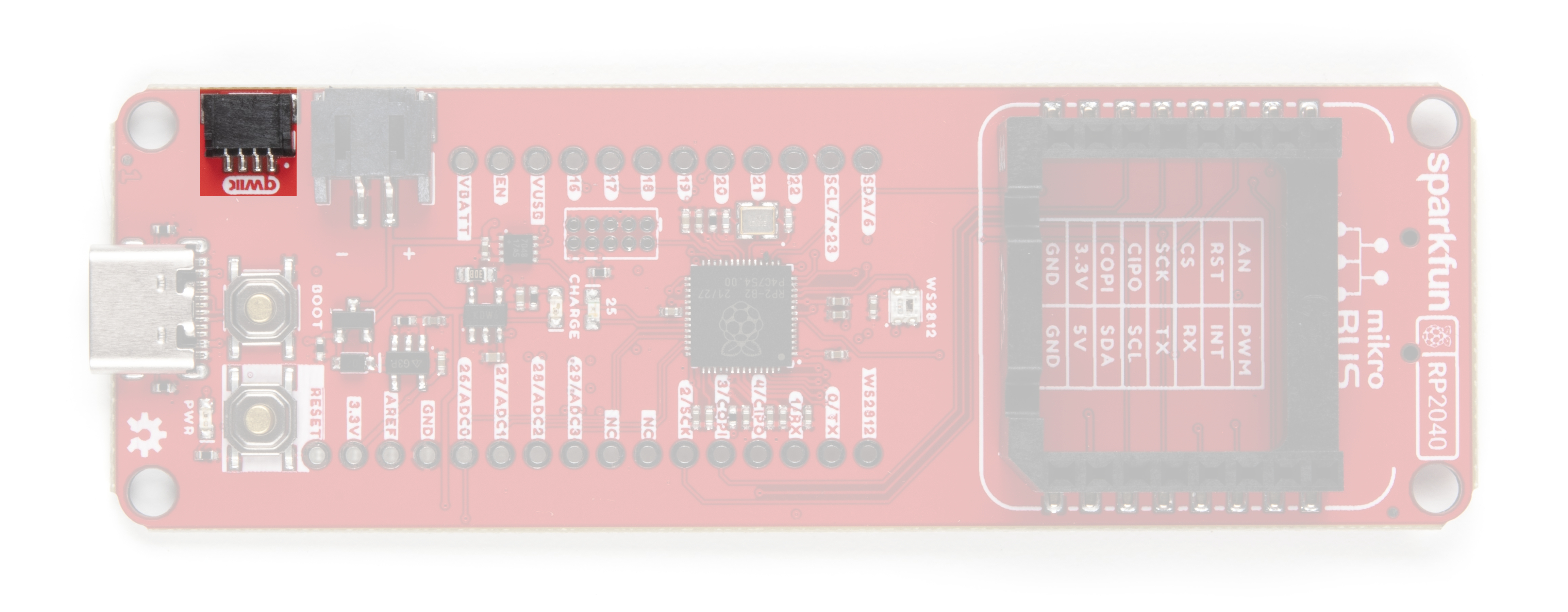
Qwiic Connector
A Qwiic connector is provided for users to seamlessly integrate with SparkFun's Qwiic Ecosystem.
What is Qwiic?
The Qwiic system is intended a quick, hassle-free cabling/connector system for I2C devices. Qwiic is actually a play on words between "quick" and I2C or "iic".
Features of the Qwiic System
Keep your soldering iron at bay.
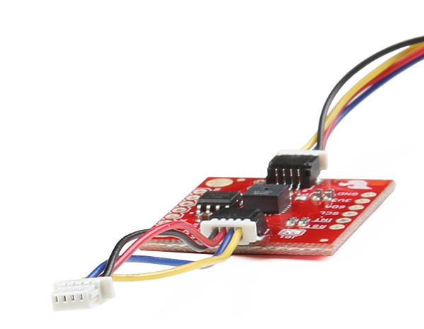
Cables plug easily between boards making quick work of setting up a new prototype. We currently offer three different lengths of Qwiic cables as well as a breadboard friendly cable to connect any Qwiic enabled board to anything else. Initially you may need to solder headers onto the shield to connect your platform to the Qwiic system but once that’s done it’s plug and go!
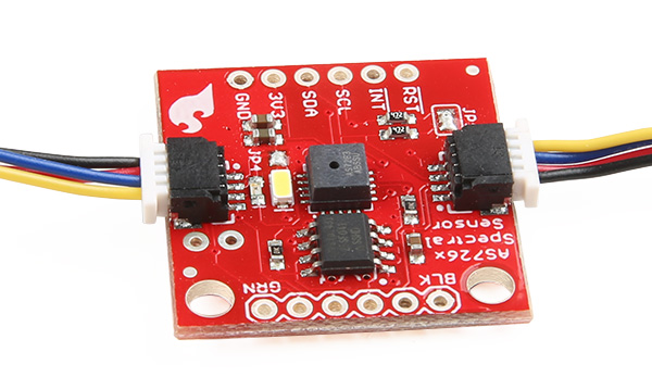
Qwiic cables connected to Spectral Sensor Breakout
Minimize your mistakes.
How many times have you swapped the SDA and SCL wires on your breadboard hoping the sensor will start working? The Qwiic connector is polarized so you know you’ll have it wired correctly, every time, from the start.
The PCB connector is part number SM04B-SRSS (Datasheet) or equivalent. The mating connector used on cables is part number SHR04V-S-B or equivalent. This is a common and low cost connector.
1mm pitch, 4-pin JST connector
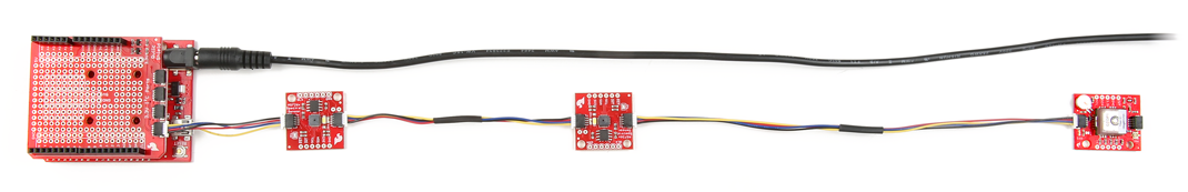
Expand with ease.
It’s time to leverage the power of the I2C bus! Most Qwiic boards will have two or more connectors on them allowing multiple devices to be connected.
I2C Jumper
Cutting the I2C jumper will remove the 4.7kΩ pull-up resistors from the I2C bus. If you have many devices on your I2C bus you may want to remove these jumpers.