Qwiic 12-Bit ADC Hookup Guide
 QCPete, santaimpersonator
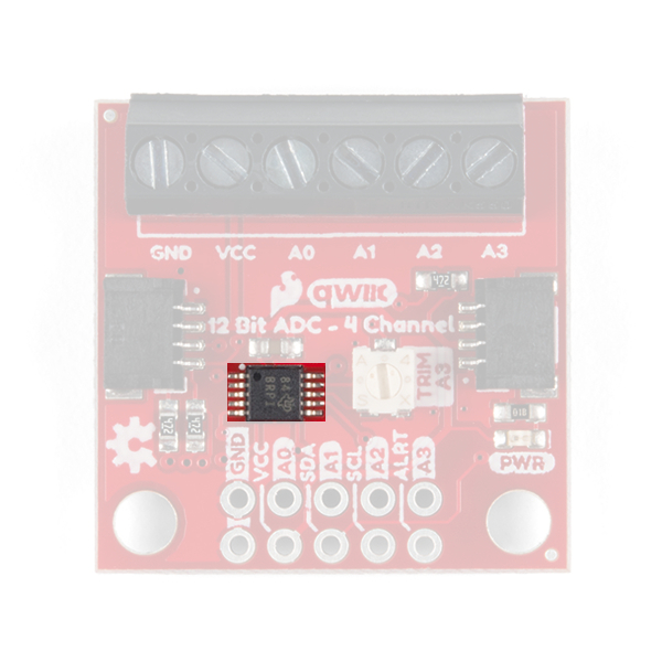
Hardware Overview
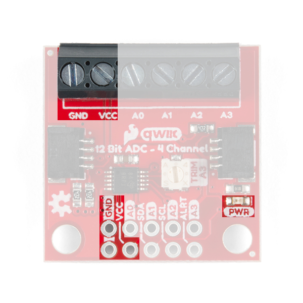
Power
There is a power status LED to help make sure that your Qwiic ADC is getting power. You can power the board either through the polarized Qwiic connector system or the breakout pins (3.3V and GND) provided. This Qwiic system is meant to use 3.3V, be sure that you are NOT using another voltage when using the Qwiic system.
(*If you want to remove the power LED to conserve power, you will need to de-solder or hotair rework the LED.)
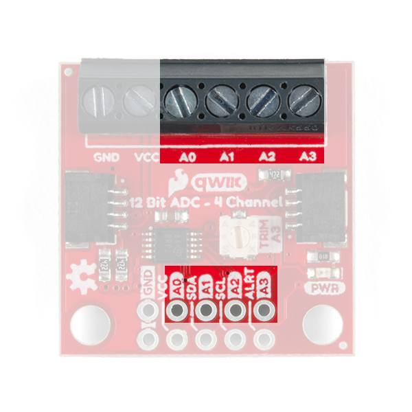
Analog Inputs
There are four input measurement channels for the ADS1015, labeled AIN0-3, accessible through the screw pin terminals shown below. With the Qwiic system, the absolute minimum and maximum voltage for these inputs is -.3V and 3.6V, respectively.
Annotated image of input connections on board.
Click to enlarge.

Example of attaching inputs through screw terminals. Click to enlarge.
Depending on the settings for the multiplexer (MUX) in the ADS1015, the analog voltage readings (or conversions on the ADC) will be either for 4 single-ended inputs or 2 differential pairs.
| Pin Label | Configuration Options |
|---|---|
| AIN0 |
Single-Ended Differential Inputs: AIN1 or AIN3 w/ Programmable Comparator |
| AIN1 |
Single-Ended Differential Ref. w/ Programmable Comparator Differential Input: AIN3 w/ Programmable Comparator |
| AIN2 |
Single-Ended Differential Input: AIN3 w/ Programmable Comparator |
| AIN3 |
Single-Ended Differential Ref. w/ Programmable Comparator On-board 10kΩ Potentiometer |
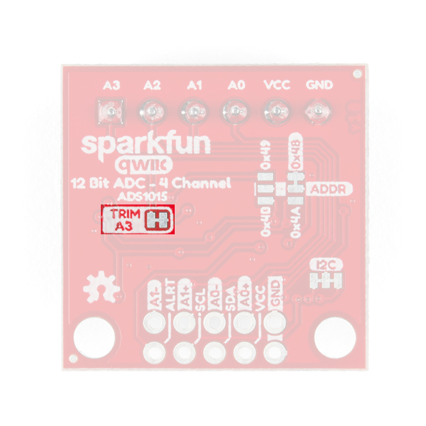
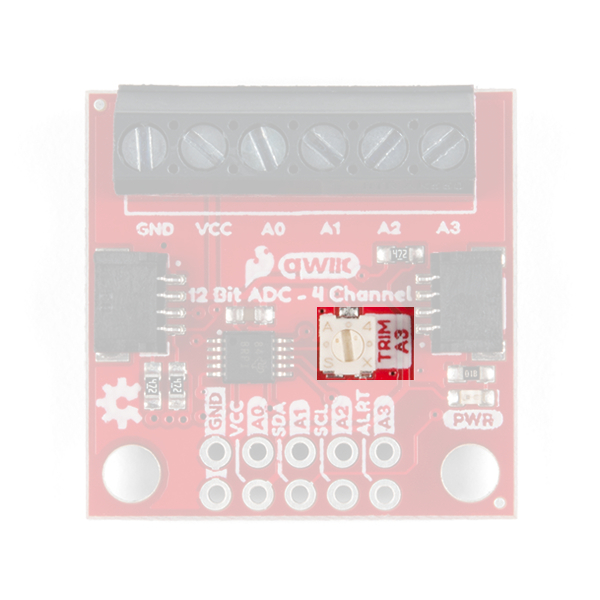
Potentiometer
In addition, there is an onboard 10kΩ potentiometer, attached to AIN3 that is used in the examples and can be used for testing. The potentiometer is connected directly to 3.3V and GND so the voltage range will always be defined by the power input to the board.
Annotated image of potentiometer on board.
Click to enlarge.
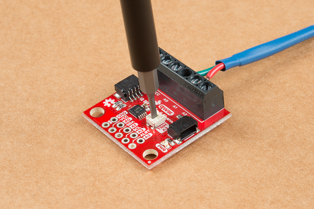
For the potentiometer, we recommend using 1.5mm flathead precision screwdriver. Click to enlarge.
ADS1015 ADC
The ADS1015 ADC is a low-power 12-bit analog-to-digital converter (ADC), which includes a built-in integrated voltage reference and oscillator. At the core of its operation, the ADC uses a switched-capactior input stage and a delta-sigma (ΔΣ) modulator to determine the differential between AINP (positive analog input) and AINN (negative analog input). Once the conversion is completed, the digital output is accessible over the I2C bus from the internal conversion register.
Annotated image of ADS1015 on board. Click to enlarge.

Functional block diagram from datasheet. Click for more details.
The ADS1015 is a powerful tool with multiple configuration settings, set by the Config Register, for the analog voltage readings (or conversions). In the following sections, we will cover the general operation of the ADS1015. For exact details of the various configuration settings, please refer to the manufacturer datasheet. The operational characteristics of the ADS1015 are summarized in the table below.
| Characteristic | Description |
|---|---|
| Operating Voltage (VDD) | 2.0V to 5.5V (Default on Qwiic System: 3.3V) |
| Operating Temperature | -40°C to 125°C |
| Operation Modes | Single-Shot (Default), Continuous-Conversion, and Duty Cycling |
| Analog Inputs |
Measurement Type: Single-Ended or Differential Input Voltage Range: GND to VDD (see Caution note, below) Maximum Voltage Measurement: Smallest of VDD or FSR Full Scale Range (FSR): ±.256V to ±6.114V (Default: 2.048V) |
| Resolution |
12-bit (Differential) or 11-bit (Single-Ended) LSB size: 0.125mV - 3mV (Default: 1 mV based on FSR) |
| Sample Rate | 128 Hz to 3.3 kHz (Default: 1600SPS) |
| Current Consumption (Typical) |
Operating: 150μA to 200μA Power-Down: 0.5μA to 2μA |
| I2C Address | 0x48 (Default), 0x49, 0x4A, or 0x4B |
Operational Modes
The ADS1015 has 2 different conversion modes: single-shot and continuous-conversion with the ability to support duty cycling. Through these modes, the ADS1015 is able to optimize its performance between low power consumption and high data rates.
Single-Shot
By default, the ADS1015 operates in single-shot mode. In single-shot mode, the ADC only powers up for ~25μs to convert and store the analog voltage measurement in the conversion register before powering down. The ADS1015 only powers up again for data retrieval. The power consumption in this configuration is the lowest, but it is dependent on the frequency at which data is converted and read.
Duty Cycling
In single-shot mode, the ADS1015 can be duty cycled to periodically request high data rate readings. This emulates an intermediary configuration between the low power consumption of the single-shot mode and the high data rates of the continuous-conversion mode.
Continuous-Conversion
In this mode, the ADS1015 continuously performs conversions on analog voltage measurements and places the data in the conversion register. If the configuration settings are changed in the middle of the conversion process, the settings take effect once the current process is completed.
Input Multiplexer (MUX)
There are four input measurement channels for the ADS1015, labeled AIN0-3. The input multiplexer controls which of those channels operates as the AINP (positive analog input) and AINN (negative analog input) to the ADC. Depending on the input MUX configuration, the voltage measurements will be either on single-ended inputs or as differential pairs.
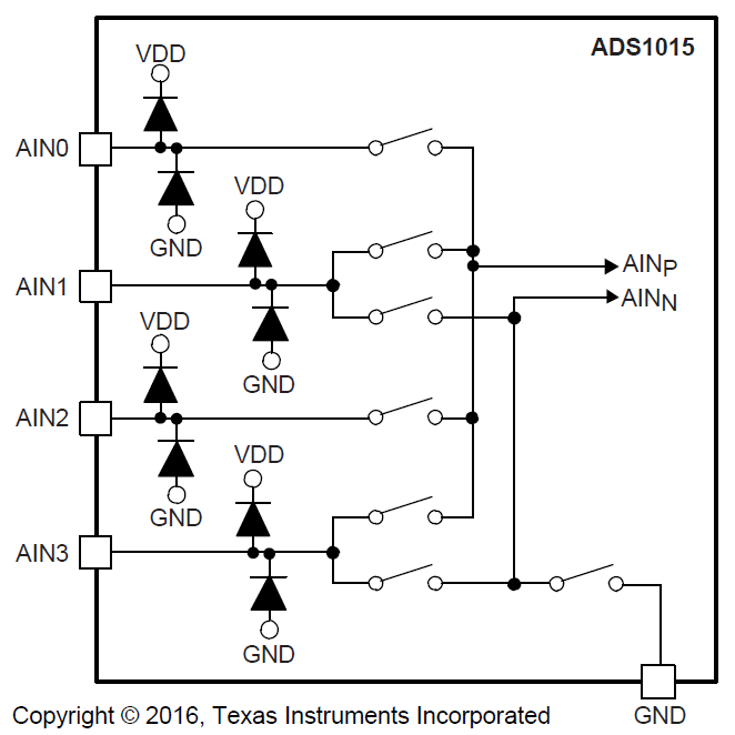
There are 8 MUX configurations to designate the analog voltage inputs to the ADC of the ADS1015, shown in the table below. The default configuration of the ADS1015 uses inputs AIN0 and AIN1 as highlighted in bold in the table below.
| Inputs | MUX Configurations | |||||||
|---|---|---|---|---|---|---|---|---|
| Differential | Single-Ended | |||||||
| AINp | AIN0 | AIN0 | AIN1 | AIN2 | AIN0 | AIN1 | AIN2 | AIN3 |
| AINN | AIN1 | AIN3 | AIN3 | AIN3 | GND | GND | GND | GND |
Programmable Gain Amplifier
A programmable gain amplifier (PGA) is implemented before the ΔΣ ADC. The ADS1015 has 6 programmable gain settings, which are expressed in the full-scale range (FSR) of the ADC scaling. The maximum analog measurement is then defined by the smaller of the FSR or VDD. By default, the ADS1015 has a resolution of 1mV by using an FSR of ±2.048V as highlighted in bold in the table below.
| Gain: | 16 | 8 | 4 | 2 | 1 | 2/3 |
|---|---|---|---|---|---|---|
| Resolution (LSB): | 0.125 mV | 0.25 mV | 0.5 mV | 1 mV | 2 mV | 3 mV |
| FSR (12-bit): | ±256 mV | ±512 mV | ±1.024 V | ±2.048 V | ±4.048 V | ±6.144 V |
Analog-to-Digital Conversion
Although, it is listed as a 12-bit ADC, the ADS1015 operates as an 11-bit ADC when used with single-ended (individual) inputs. The 12th bit only comes into play in differential mode, as a sign (+ or -) indicator for the digital output. This allows the digital output to represent the full positive and negative range of the FSR (see table and figure below).

Limitation of ADS1015
Since the ADS1015 only uses an internal reference voltage, the FSR is to be defined by the design of the 12-bit ADC:
FSR = LSB x 212
where, the LSB = 0.125, 0.25, 0.5, 1, 2, or 3 mV.
Due to the configuration options, it is difficult to make full use of the full-scale range of the ADS1015 with common (useful) voltages. See the examples below for a more detailed explanation:
If the FSR = 2.048V and VDD = 3.3V:
- Resolution of the digital data: 1mV (defined by FSR)
- Input voltage range: 0-3.3V (defined by VDD)
- Data Range: 0000h-7FF0h (HEX) or 0-2.048V The range of the input voltage that can be read by the ADC is limited by FSR. Any voltage higher than the FSR (but less than VDD) reads the same maximum value in the digital output because the FSR is maxed out. In this case, you are maximizing the resolution (use of the data output), but not the full, allowable range of analog input (0-3.3V).
If the FSR = 4.096V and VDD = 3.3V:
- Resolution of the digital data: 2mV (defined by FSR)
- Input voltage range: 0-3.3V (defined by VDD)
- Data Range: 0000h-0672h (HEX) or 0-3.3V The data range is limited by VDD, any higher input voltage will continue to have data up to the electrical specifications of the ADS1015 ~VDD + 0.3V, where the IC gets damaged. In this case, the input voltage is being maximized to the electrical specification (0-3.3V). However, this means you are effectively only using 80% of the full resolution of the ADC (i.e. a 10.8-bit ADC at 3.3V).
Data Rate & Conversion Time
The ADS1015 offers 7 selectable output data rates of 128 SPS, 250 SPS, 490 SPS, 920 SPS, 1600 SPS, 2400 SPS, or 3300 SPS. Conversions for the ADS1015 settle within a single cycle; thus, the conversion time is equal to 1/DR.
Programmable Digital Comparator
The ADS1015 features a programmable digital comparator that can trigger the ALERT/RDY pin to indicate when conversion data is ready. By default, the comparator is disabled. However, when activated, the comparator operates in either a traditional or window mode. The upper and lower thresholds for the comparator are set by the last two registers on the ADS1015; while, the polarity (active low/high), latching or non-latching, operational mode, and enabling of the ALERT/RDY pin are set in the Config register.
Qwiic or I2C
I2C Address
The ADS1015 has 4 available I2C addresses, which are set by the address pin, ADDR. On the Qwiic ADC, the default slave address of the ADS1015 is 0x48 (HEX) of 7-bit addressing, following I2C protocol. The ADS1015 does have an additional general call address that can be used to reset all internal registers and power down the ADS1015 (see datasheet).
Default I2C Slave Address: 0x48
I2C Registers
The ADS1015 has four 16-bit registers, which are accessible through the I2C bus using the Address Pointer register. The Address Pointer register is an 8-bit byte that is written immediately after the slave address byte, low R/W bit.
| Address | Description |
|---|---|
| N/A | Address Pointer Register (8-bit): Used to grant R/W access to the four available registers on the ADS1015. |
| 0x00 | Conversion Register (16-bit): Contains result of last conversion (i.e. measurement). |
| 0x01 | Config Register (16-bit): Used the for configuration setting of the ADS1015. |
| 0x02 | Low Threshold Register (16-bit): Low threshold value for digital comparator. |
| 0x03 | High Threshold Register (16-bit): High threshold value for digital comparator. |
Connections
The simplest way to use the Qwiic ADC is through the Qwiic connect system. The connectors are polarized for the I2C connection and power. (*They are tied to their corresponding breakout pins.)
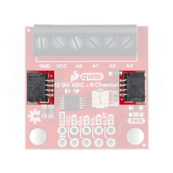
However, the board also provides five labeled breakout pins. You can connect these lines to the I2C bus of your microcontroller and power pins (3.3V and GND), if it doesn't have a Qwiic connector. The ALERT/RDY pin is broken out to use for triggered events (requires pull-up resistor).
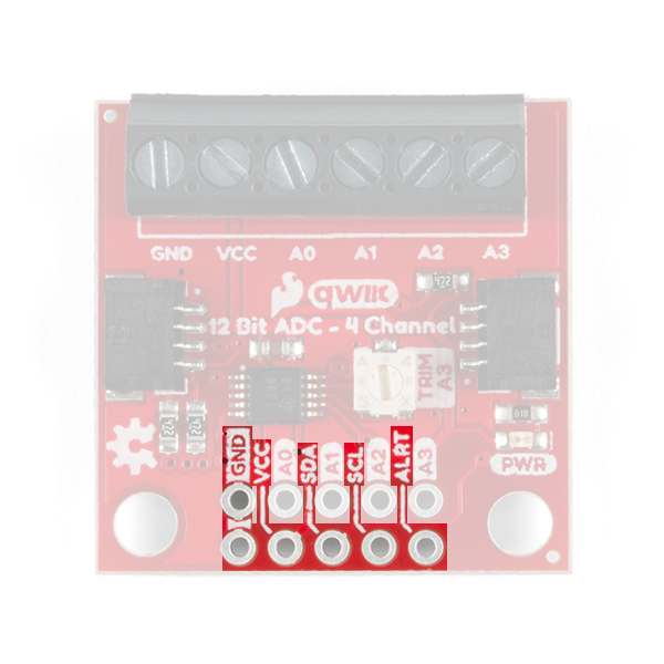
| Pin Label | Pin Function | Input/Output | Notes |
|---|---|---|---|
| 3.3V | Power Supply | Input | 3.3V on Qwiic system (should be stable) |
| GND | Ground | Input | Ground and Single-Ended Reference Voltage for ADC. |
| SDA | I2C Data Signal | Bi-directional | Bi-directional data line. Voltage should not exceed power supply (e.g. 3.3V). |
| SCL | I2C Clock Signal | Input | Master-controlled clock signal. Voltage should not exceed power supply (e.g. 3.3V). |
| ALERT/RDY | Alert/Interrupt | Output | Comparator |
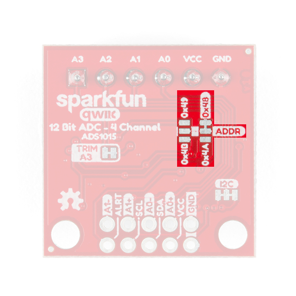
Jumpers
There are jumpers on the board allowing the user to select between different I2C addresses, to remove the pull up resistors from the I2C pins, and to disconnect the potentiometer on AIN3. Not sure how to modify a jumper? Read here!
I2C Address
The ADS1015 has four available I2C addresses, which can be configured by the jumpers on the back of the board. The address selection pin is connected to the center pad of the jumpers, the below table shows the addresses available when the address selection pin is tied to each of the 4 available pads.
| Pin | GND | VCC | SDA | SCL |
|---|---|---|---|---|
| Address | 0x48 (Default) | 0x49 | 0x4A | 0x4B |
The address selection pin, by default is tied to GND on the PCB. Cutting the trace and bridging the I2C address jumper to another pad changes the slave address from I2C Jumper Default: 0x48. The location of the jumpers is shown in the image below.
I2C Pull-up Jumper
Cutting the I2C jumper will remove the 2.2 kΩ pull-up resistors from the I2C bus. If you have multiple devices with pull-up resistors on your I2C bus, you may want to cut these jumpers. (When there are multiple devices on the bus with pull-up resistors, the equivalent parallel resistance may create too strong of a pull-up for the bus to operate correctly.)
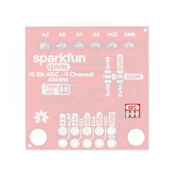
Potentiometer
Cutting the potentiometer jumper will disconnect 10kΩ potentiometer from the AIN3 input pin.