Proto Pedal Example: Programmable Digital Pedal
 Byron J.
Assembly Part 1 (power and analog section)
The Jumping Off Point
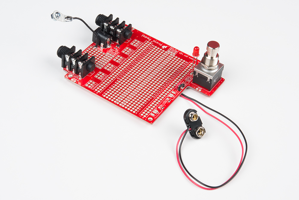
To begin, we'll assume that you've completed the basic assembly of the proto pedal board.
One detail worth noting is that you can likely omit the 9V battery snap. While it's possible to power this pedal from a 9V battery, the Teensy is thirsty for current, and you can expect 6 to 10 hours battery life. An external power supply is highly recommended!
If you're using the Proto Pedal Chassis, you'll need to prepare it by drilling holes for five potentiometers, and holes for programming the Teensy. This is the chassis shown in the Chassis hookup guide.
With the prerequisites complete, you can start the sequence below. We'll build the circuit in four major stages: the voltage regulator, the analog section, the Teensy, and the panel controls. We're going to be stepping fairly quickly. Each step lists the required components, so you can prepare them before you commence. Once they have been placed, double-check your solder joints, and compare your work to the photos. Each of the four stages ends with a short test, to test out the results of that stage.
Grid Notation
In the following steps, we're going to use the grid notation seen on a standard solderless breadboard. From left to right, the columns are numbered 1 to 30, and from bottom to top, the rows are assigned letters from A through J. Any hole in the center of the board can be referenced by number-letter coordinate, such as 27L or 7G.
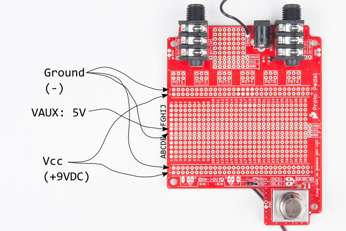
We'll also be using both of the center rails of the proto area. The upper one will be tied to VAUX, the output of the 5V voltage regulator, and the lower one will be tied to ground.
Power Section
Teeny expects an input voltage in the 3.6 to 6.0 VDC range. We'll create a new supply rail for that voltage, using the power section between the input and output jacks, which we'll route to the VAUX trace at the center of the board.
The area near the top of the board has a 7 x 7 grid of pad-per-hole prototying area, plus rails for VCC and ground across the bottom.
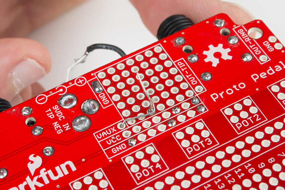
We'll start with a LM7805 voltage regulator, and two 10 uf capacitors.
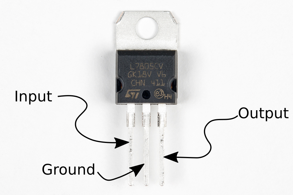
To fit the voltage regulator into this area, we'll bend the legs as follows.
- The output, leg 3, is bent straight down along the body of the regulator.
- The input, leg 1, extends one grid space beyond the body before being bent down.
- The ground, leg 2, is one grid space longer than leg 1.
This contortion is illustrated in the photo below.
Note the staggered legs of the regulator.
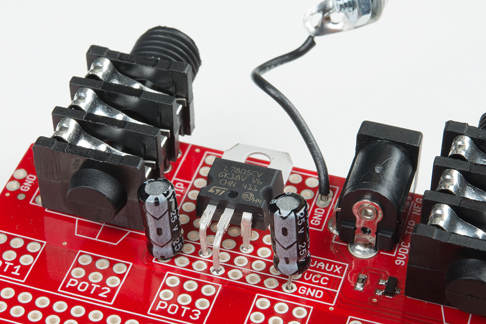
There are also two 10 uf capacitors in this area.
| Capacitor Value | Value Marking | Start Coordinate | End Coordinate | Orientation Notes |
|---|---|---|---|---|
| 10 uf electrolytic | 10uf/25V | Ground rail atfar left | VCC rail at far left | `-` to ground rail |
| 10 uf electrolytic | 10uf/25V | ground rail at far right | VAUX pad at far right | `-` to ground rail + lead extends from VAUX to regulator output terminal. |
The cap on the VAUX rail has a special trick: its positive leg ls run underneath the board, to the output of the voltage regulator, before being soldered in place at both the VAUX pad and the regulator pin. After soldering, trim the excess leads of both the cap and regulator.
Incremental Test
With the regulator and caps in place, we can test the voltage regulator.
Apply 9V power to the board, connect a TS jack to the input, and measure the VAUX pin. It should be in the range of 4.9 to 5.1 VDC.
Before moving on to the next step, be sure to remove power from the unit.
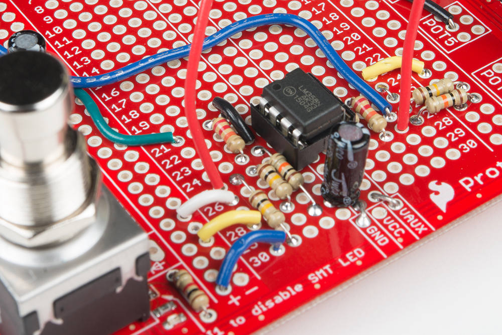
Analog Section
With the regulator tested, we can move on to the analog portion of the circuit. We'll start by placing a bunch of jumpers, then add resistors and caps, finally the IC.
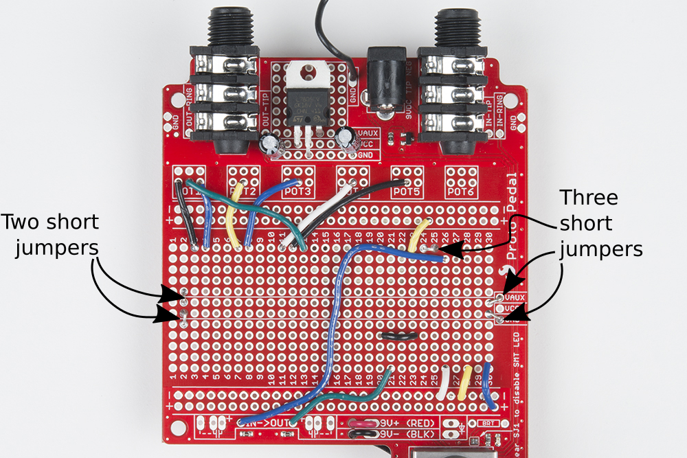
Jumpers
The analog section of the circuit has nineteen jumpers. We used multicolored solid-core 22 gauge wire. For clarity in the photos, we're not using any red wire.
| Jumper Number | Color | Start Coordinate | End Coordinate |
|---|---|---|---|
| 1 | Black | 3J | Pot1 Left |
| 2 | Blue | 4J | Pot1 Right |
| 3 | Yellow | 7J | Pot2 Middle |
| 4 | Blue | 8J | Pot3 Middle |
| 5 | White | 11J | Pot4 Middle |
| 6 | Black | 12J | Pot5 Middle |
| 7 | Green | 13J | Pot1 Middle |
| 8 | Yellow | 23J | VCC |
| 9 | White | 26A | Ground |
| 10 | Blue | Input | 26I |
| 11 | Green | 21A | Out |
| 12 | Black | 21D | 23D |
| 13 | Yellow | 28A | Ground |
| 14 | Blue | 30A | Vcc |
| 15 | Bare | 2F | VAUX |
| 16 | Bare | 2E | Ground |
| 17 | Bare | 24J | 25J |
| 18 | Bare | VAUX | Top Center Rail |
| 19 | Bare | Ground | Bottom Center Rail |
With the jumpers in place the board will look like this
(Click to enlarge).
R's & Cs
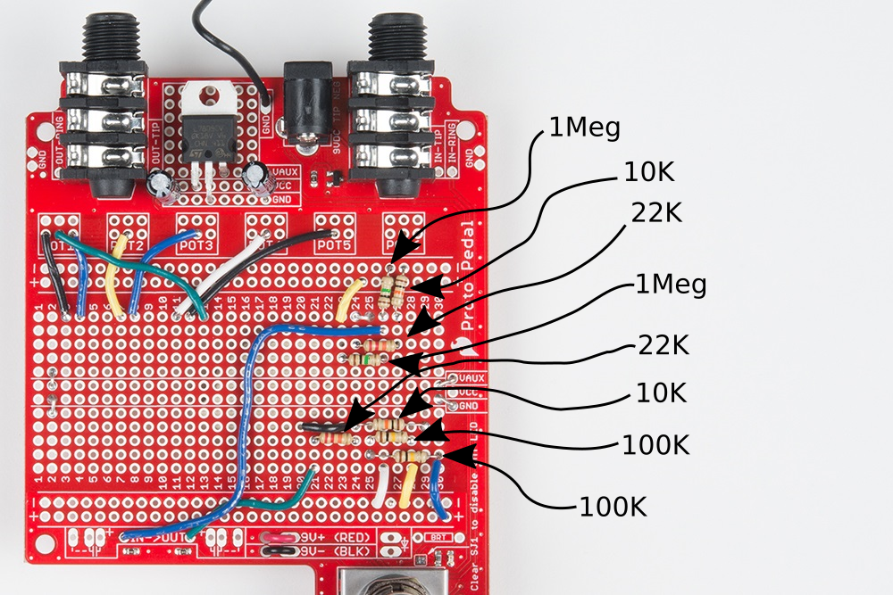
Next we'll install the passive analog components, the resistors and capacitors.
There are eight resistors. Most are folded to 0.3" long, with the legs bent right at the ends of the body. One 10K and one 100K are 0.5" long, as noted in the placement column below.
| Resistor Value | Value Color Code | Start Coordinate | End Coordinate | Placement Notes |
|---|---|---|---|---|
| 1M Ω | brown-black-green-gold | 26J | Upper Ground | |
| 10K Ω | brown-black-orange-gold | 27J | Upper Ground | |
| 22K Ω | red-red-orange-gold | 24H | 27H | |
| 1M Ω | brown-black-green-gold | 23G | 26G | |
| 22K Ω | red-red-orange-gold | 21C | 24C | |
| 10K Ω | brown-black-orange-gold | 24D | 29D | 0.5" long |
| 100K Ω | brown-black-yellow-gold | 25C | 28C | |
| 100K Ω | brown-black-yellow-gold | 25B | 30B | 0.5" long |
(Click to enlarge).
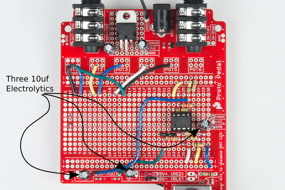
There are three 10 uf electrolytic capacitors. Take note of the polatiry - the negative leg is marked on the body of the cap with a stripe, which is also visible in the photo below.
| Capacitor Value | Value Marking | Start Coordinate | End Coordinate | Orientation Notes |
|---|---|---|---|---|
| 10 uf electrolytic | 10uf/25V | Input Coupling | `-` to left | |
| 10 uf electrolytic | 10uf/25V | 29E | Center ground | `-` to top |
| 10 uf electrolytic | 10uf/25V | Output Coupling | `-` to right |
(Click to enlarge).
Op-amp
The last component in the analog section is the operational amplifier.
| Component | Marking | Start Coordinate | End Coordinate | Orientation Notes |
|---|---|---|---|---|
| DIP-8 IC Socket for LM358 | Row 23 | Row 26 | Spanning center trough Notch facing left |

(Click to enlarge).
After soldering the socket, insert the LM358, again with the notch facing to the left.
Incremental Test
To test this stage, we'll install one extra, temporary wire, from 25A to 27I, the red wire shown below. This ties the input amplifier to the output amplifier.
Apply power to the circuit, then connect the input and output. We used a signal generator and an oscilloscope. If you don't have them handy, you can use a guitar and amplifier -- just be careful to keep the volume low until you're certain that the circuit is well behaved.
While applying input signal, press the stomp switch. Aside from the slight click when the switch engages, the output signal should be nearly the same with the pedal active or bypassed.
Again, disconnect power before moving on, and also remove the temporary jumper.