Proto Pedal Assembly and Theory Guide
 Byron J.
 Introduction
The SparkFun Proto Pedal is a PCB that makes building guitar effect pedals easier.
Lets face it, most guitar pedals start with similar circuitry -- you need the input and output jacks, the bypass switch (hopefully with a status LED), and a barrel jack for power input. In some circuits, there may be as much wiring involved in the jacks and switch as there is in the effect itself.
This PCB handles all of the essential jack and switch related wiring. It offers:
- True bypass and LED switching with a heavy-duty three pole, double throw (3PDT) stomp switch.
- Prototyping area equivalent to a standard solderless breadboard.
- Some extra proto area for power regulation or reference voltages.
- Six positions to help organize potentiometer wiring.
To protect the PCB from the hazards of stage and studio, we've also got an optional, matching, pre-drilled die cast enclosure.
This guide will show you how to assemble the PCB, then explain the I/O, power, and switching circuits. If you're new to building guitar pedals, this guide should help you get started. If you're experienced with electronics, but new to guitar pedals, you might want to check out the prototyping and theory sections, because guitar pedals employ some clever and unique circuit conventions.
The upside is that it's compatible with nearly any pedal power supply, such as the Boss PSA Adapter, or the Voodoo Labs Pedal Power supply.
Suggested Reading
- Learn about the various types of switches available.
- Some background on using solderless breadboards as well as Printed Circuit Boards - PCBs.
- There are many websites the discuss the design and construction of guitar effects. A couple of the author's favorites are Geofex and AMZ.
Assembly Instructions
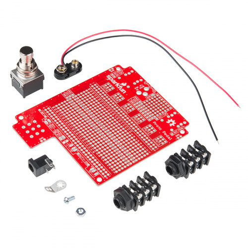
Parts
In the Proto Pedal box, you will find the following pieces.
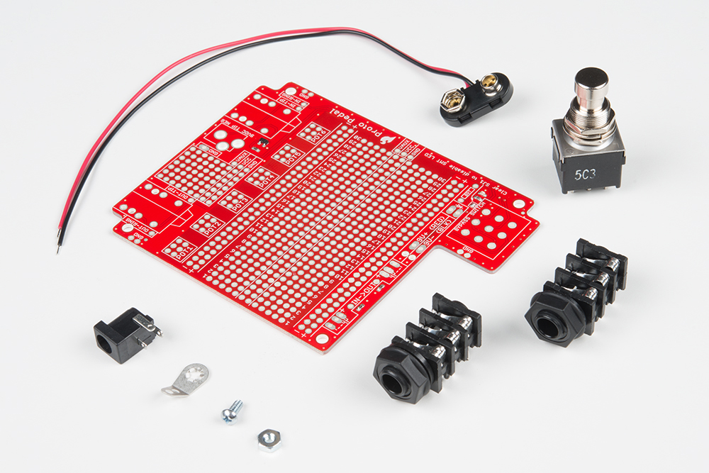
Clockwise from the top left, you see:
- One heavy-duty 9 Volt battery snap.
- One 3PDT stomp switch.
- Two TRS jacks.
- One each 4-40 nut, machine screw and star washer ground lug.
- One 2.1mm Barrel jack
- One PCB with SMT work completed
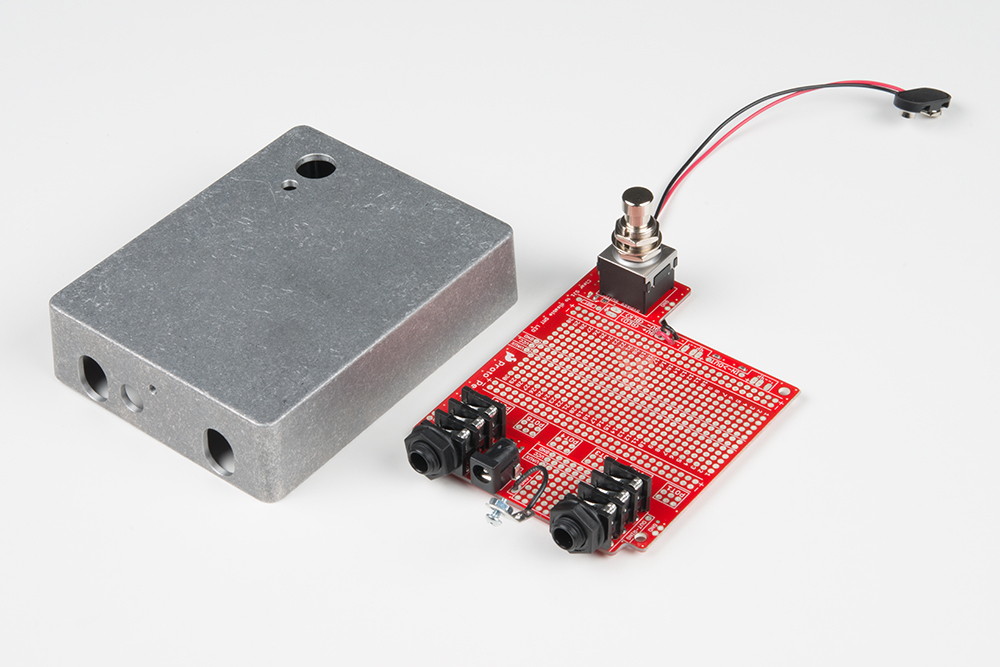
Additionally, we highly recommend the pre-drilled chassis. It's a standard sized cast aluminum box, which does double duty as an assembly jig, to help get the jacks and switch aligned correctly.
You'll also need a short piece of stranded hookup wire.
Tools
To assemble the Proto Pedal, we recommend the following tools and materials:
- Soldering Iron
- Lead-based or Lead-free solder
- Diagonal or Flush cutters
- Small Philips Screwdriver
Assembly
The first step of assembly is deciding whether or not you're using the pre-drilled chassis. There are a couple of assembly steps that are determined by the chassis.
- First, if you're building with the chassis, it serves as an assembly jig for some components. The walls of the chassis sit at a slight angle, so when the TRS jacks meet the walls properly, they don't sit completely flush with the board.
- Second, when sealed up in the chassis, the onboard surface mount LED is hidden. There's a position for an optional 5mm PTH LED. You're welcome to pick your favorite color and select a 1/4W PTH bias resistor for the LED. For this guide, we're using a 5mm Red LED and a 1K Ω resistor.
If you're not using the chassis, you can mount the jacks flush on the board, and the SMT led will suffice for bench testing.
Jacks and Switch
If you're building the pedal with the chassis, the first step is to mount the switch and jacks to the box.
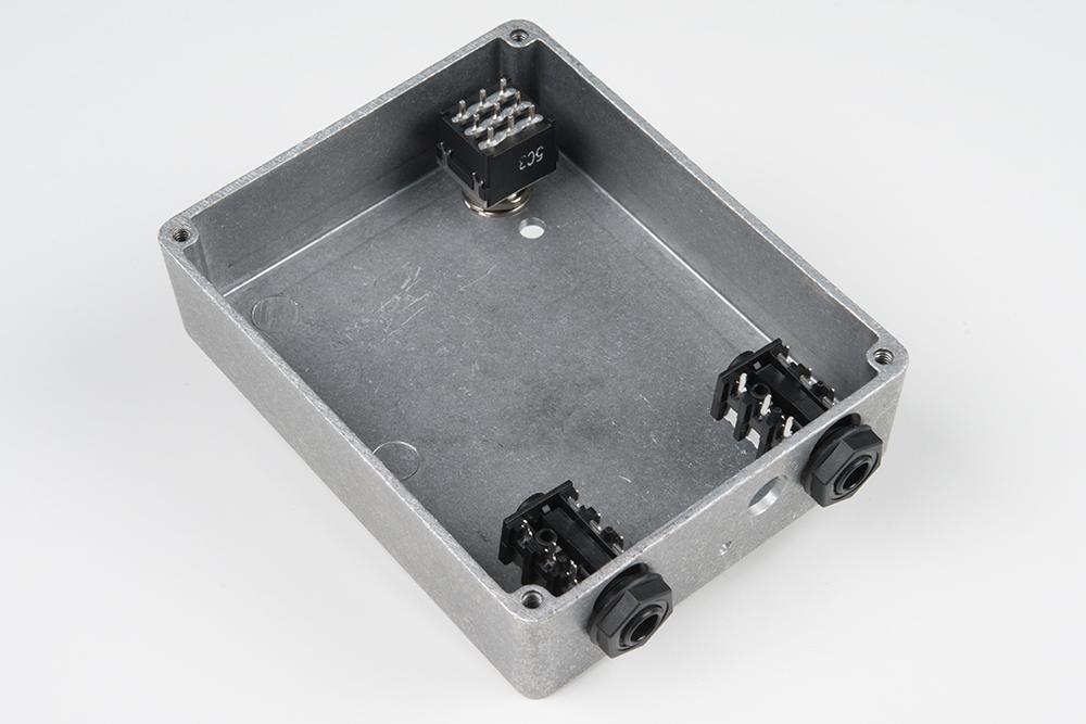
The jacks each have a plastic nut and a washer, which should both be threaded on from the outside of the box.
The switch has two nuts, a smooth washer, and a lock washer. Remove one nut and both washers, then set the remaining nut about 0.125" (3mm) from the body of the switch, as shown below.
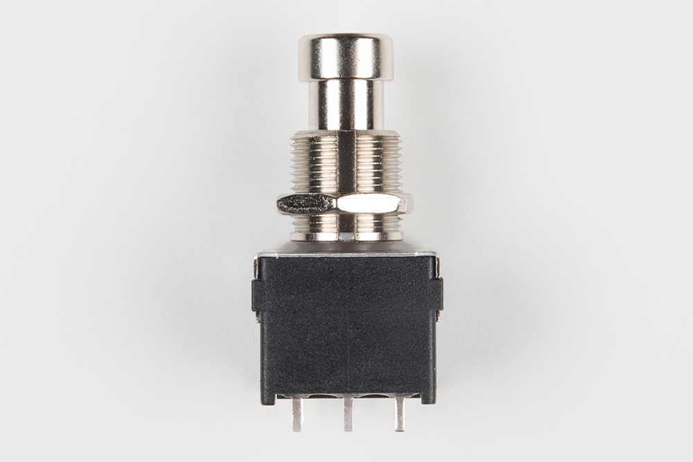
Put the lock washer on the switch, then put the switch through the chassis. On the external side of the switch, put on the smooth washer, and finally the other nut.
Tighten the nuts on the jacks and switch so they stay in place but can still rotate in the holes. Having a little bit of play in them helps get the PCB aligned properly.
Slide the printed circuit board onto the legs of the jacks and switch.
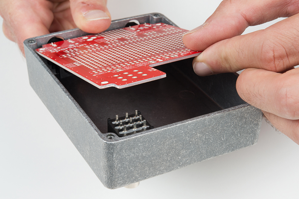
Taking care to keep the TRS jacks near the top of the oblong holes, tighten the nuts on the jacks and switch with your fingers. Due to the sloped side of the enclosure, the legs of the jacks that are nearer the center of the board will protrude further than those near the edge.
Solder the jacks and switch to the PCB.
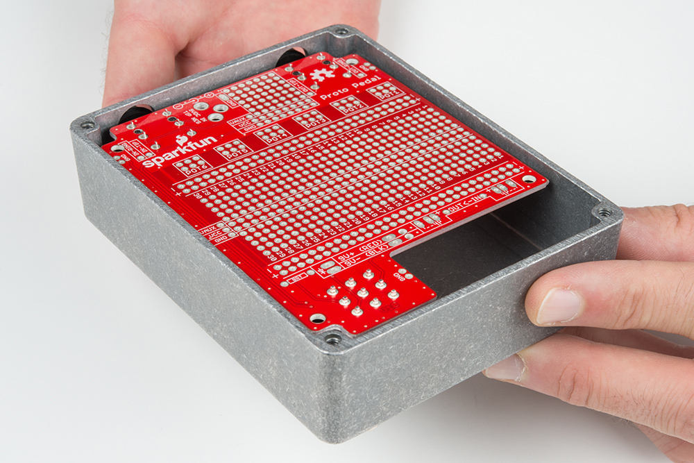
Remove the PCB from the chassis, and put on the last few touches.
To remove the PCB from the chassis, undo the nuts on the jacks and switch. Then, press the switch, and the whole assembly will pop free.

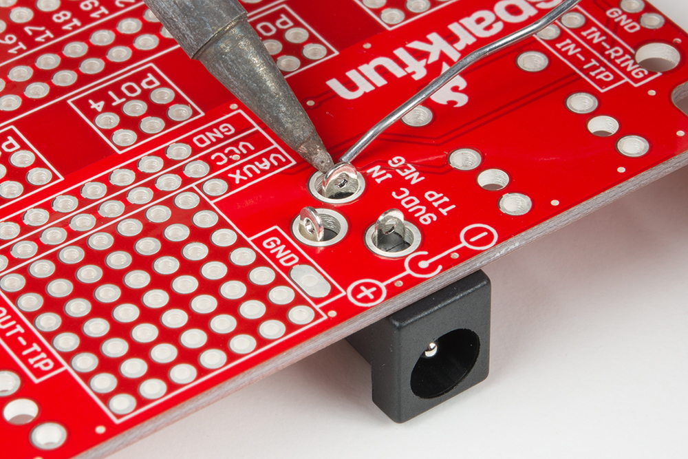
Power Input Jack
The next step is soldering the barrel jack, which goes between the TRS jacks.
5mm LED.
If you're adding a through-hole LED, it goes next to the stomp switch, and the bias resistor goes next to it in the resistor location marked BRT. To make it through the hole in the chassis, the LED needs to stand some distance from the PCB. As with the switch and jacks, you can use the chassis as a template to get it aligned correctly.
The LED is polarized and needs to be installed correctly. The cathode of the LED is marked by both the flat spot on the collar of the LED and the shorter leg, which should face towards the switch.

With the LED and resistor soldered in place, trim the legs flush with the bottom of the PCB.
You can also remove the solder blob from SJ1, near the bias resistor, to disable the internal LED.
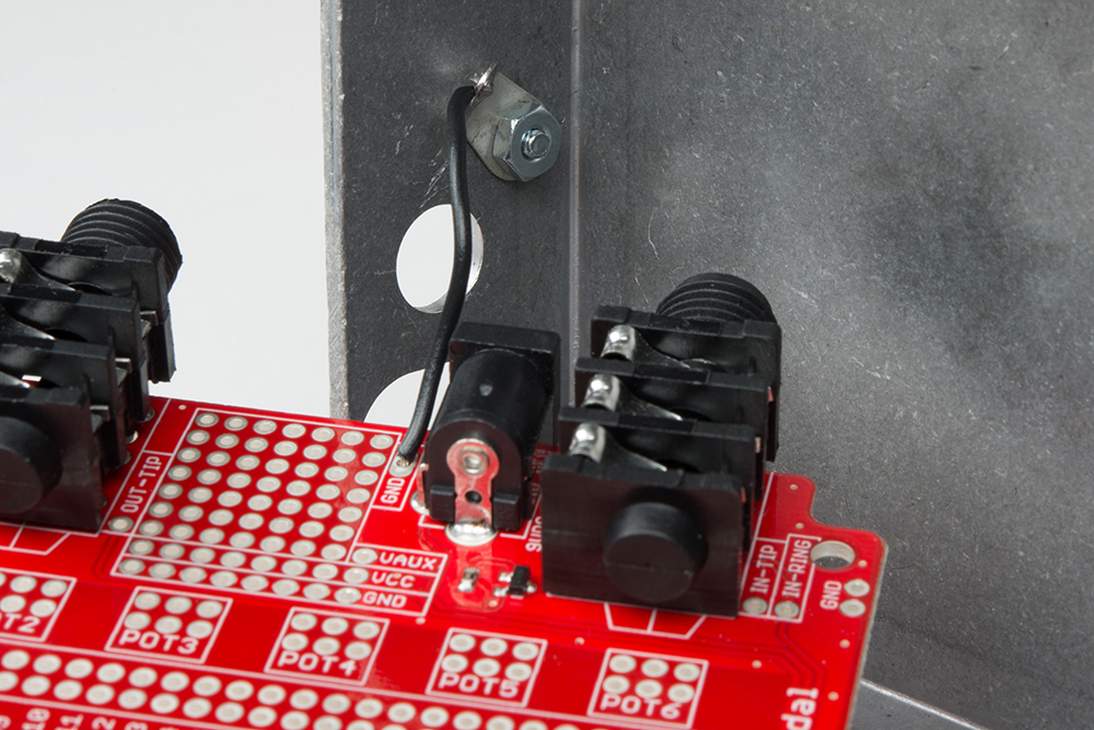
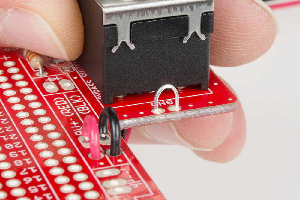
Chassis Ground Lug
Next, add the ground lug.
You'll need a short piece of stranded hookup wire. Strip and tin the ends of the wire. Solder one end to the ground pad near the barrel jack and the other end to the star washer.

The star washer mounts to the chassis via the small hole near the barrel jack.
9V Battery Snap
Finally, solder in the 9V battery snap. The PCB has some additional holes to relieve stress on the battery wires -- feed the wires up through the holes, then back through the solder pads. Take care to match the wires, red, and black, to the legend on the board.
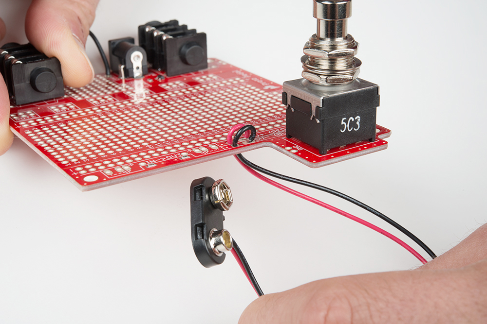
The battery snap is optional -- if you're strictly using an external power supply, you might prefer to leave it off so there isn't a loose connector wandering around in the box.
Prototyping With The Proto Pedal
While you're developing your circuit, you can place a solderless breadboard over the center of the board.
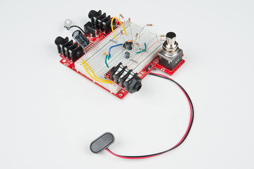
When you're ready to finalize the design, you can transcribe the circuit onto the Proto Pedal PCB. The connections in this area of the PCB duplicate those on the solderless board.
There is one difference between the breadboard and Proto Pedal layout, though. There are two additional side-to-side traces down the center of the proto area.
These traces aren't assigned to any specific signal, but can be easily tied to VCC, GND, or VAUX using the pads at the left edge of the board. We'll discuss VAUX shortly.
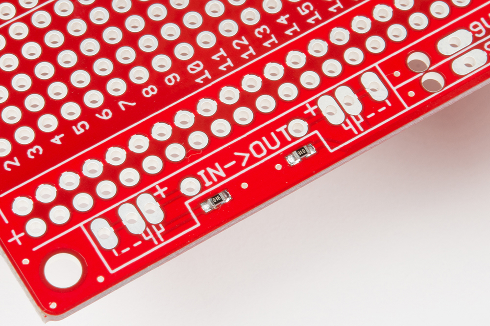
Coupling Caps
The input and output to a guitar pedal circuit almost always use coupling capacitors at the input and output. There are footprints for these caps near the lower edge of the PCB.
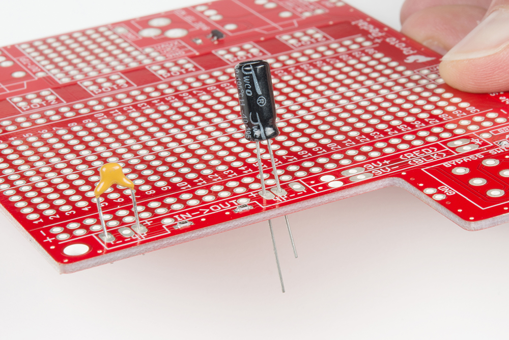
Not every circuit uses the same value, size or composition of capacitor. Therefore, these footprints are designed to accommodate a variety of lead spacing. These locations fit both 2mm and 5mm caps, as shown above.
If you're using polarized coupling caps, the + leads usually face the circuit input/output pads, as marked on the PCB.
Your Circuit Goes Here
With the coupling caps in place, the input and output to the heart of the circuit are the through-hole pads between the coupling caps, marked IN and OUT.
Adding Knobs
The PCB also has six positions for adding potentiometers.
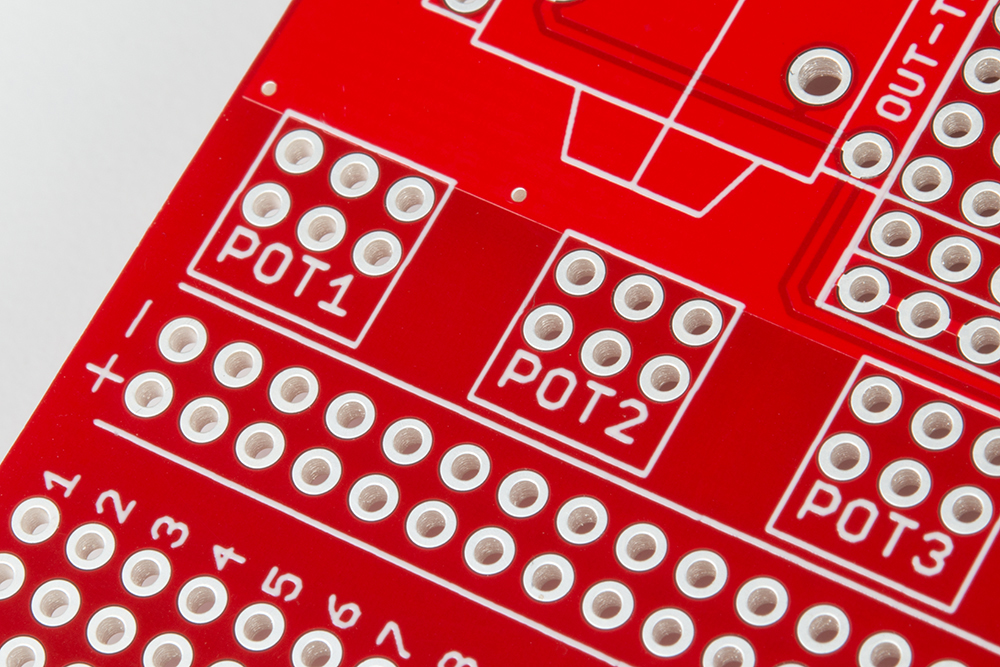
The intent of these positions is that you can run short wires from the proto area to the lower row of pads, then run longer wires from the top pads to the pots, which are bolted to the chassis. This helps keep the proto area tidy.
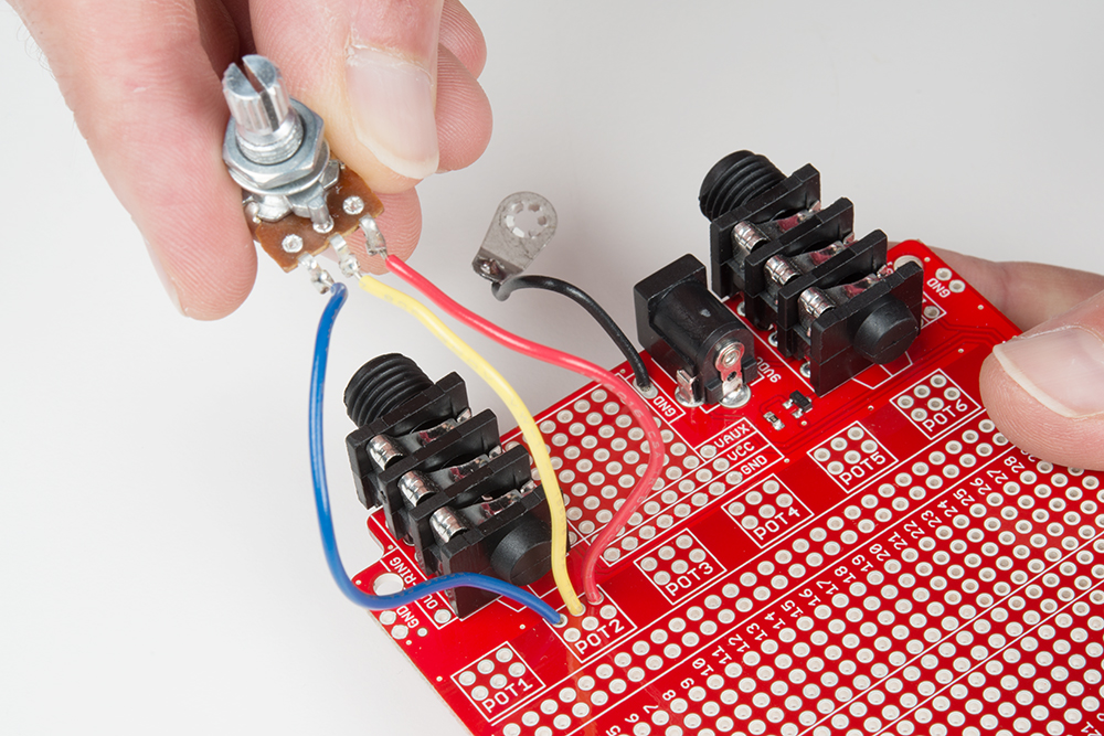
The concept of leaving the wires a little long is known as a "Service Loop" -- the system can be disassembled and the PCB can be accessed without having to take the pots off the front panel or disconnect any wires.
Power Supply Area
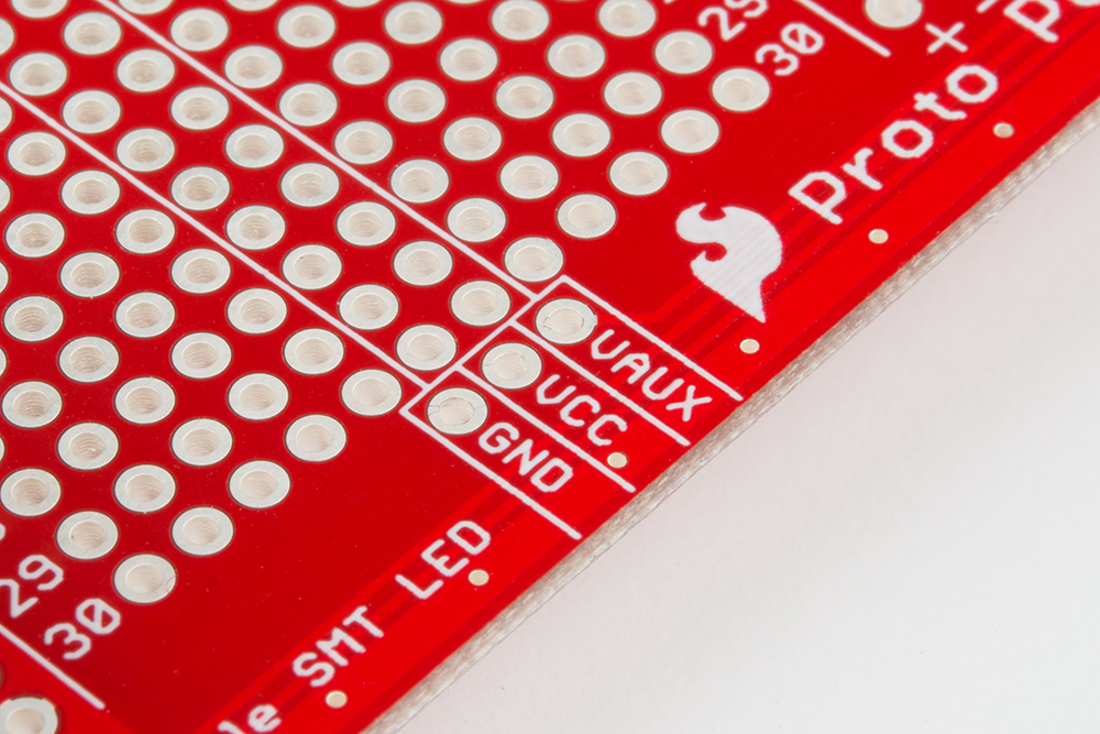
There is an extra pad-per-hole proto area between the TRS jacks. This area is intended to allow you to add extra circuitry, such as a voltage regulator or rail splitter. If you're really ambitious, you could build a charge pump circuit in this area, to generate bipolar power supply rails.
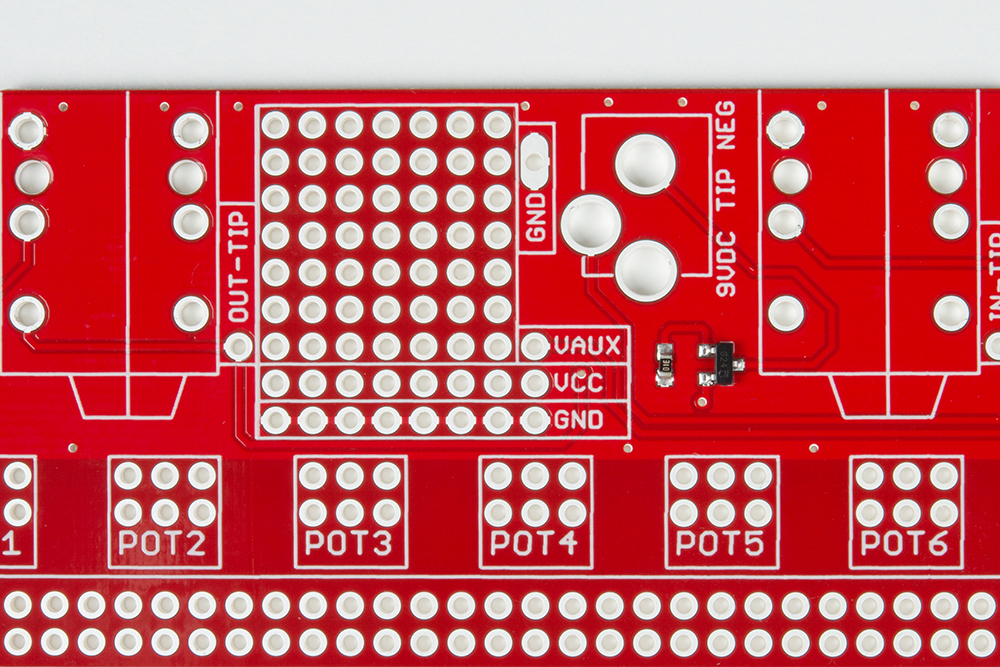
If you're deriving a new voltage rail, there is also an uncommitted trace from this area to the proto area, marked VAUX, for "auxillary voltage."
The three connections at the lower left of this area (VAUX,VCC,GND) run to the similarly named set of pads to the right of the prototyping area.
Prototyping Area
The center of the board is the same as a medium-sized solderless breadboard.
Across the top and bottom of this area are power supply traces that run from side to side. The Trace marked + is tied to VCC, and the trace marked - is tied to ground. Between the power traces are pairs of five-pad vertical groupings, arranged in 30 columns. Typically, a dual-in-line (DIP) IC package is placed so it spans the gap at the center of the board.
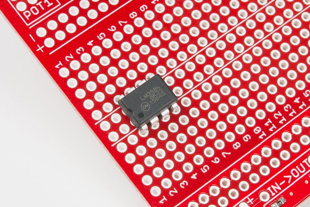
Each leg of the IC is then electrically continuous with the remaining four holes in the group. A short wire can be used as a jumper to connect pads to the power rails, and passive components like capacitors and resistors can be inserted between rows to make connections.
Extra Lateral Traces
On an ordinary DIP-IC prototyping board, the space down the center of the proto area (between the two sets of pads) is empty. The Proto Pedal has an extra pair of traces running in this area.
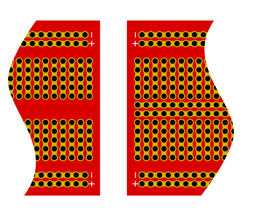
These traces simply run from left to right -- you can decide how they're used in your design. For convenience, VCC, Ground and VAUX can be found on pads near the right end of these traces and can be jumpered to the center traces.
We'll show an example that uses these traces in the EQ Pedal project.
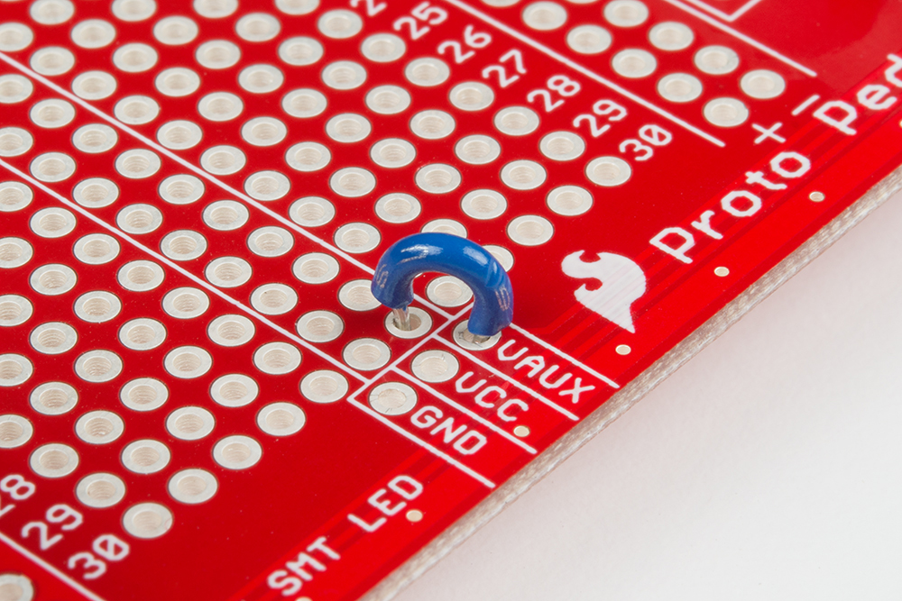
Ground Lugs and Test Points
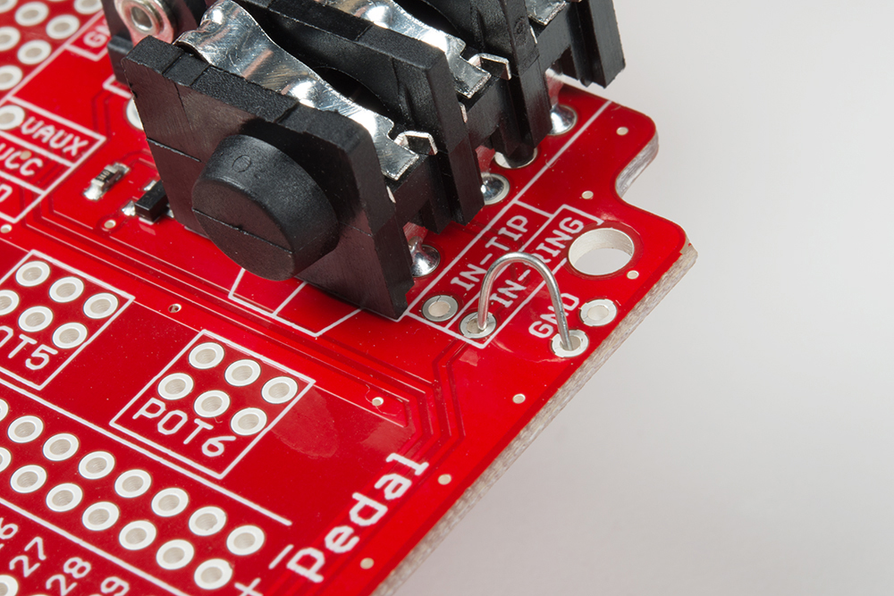
There are a number of extra through hole pads on the PCB. There are several pairs of ground pads, which can be populated with small wire loops so you can clip a multimeter or oscilloscope probe ground to them.
There are also test points providing access to the tip and ring of the input and output, adjacent to their respective jacks. The ring of the input jack can be found near the ground connection at the top-right corner of the board -- if you need to power the pedal even when the input jack is unplugged, you can run a piece of wire between them. Just don't forget to remove it before deploying the pedal, or your battery life will suffer!
It Reads From Right-To-Left
When seen from the user's perspective, the Proto Pedal is on the floor near their feet, with the stomp switch facing towards them and the jacks facing away.
In another puzzling but long-standing FX pedal convention, viewed this way, the input jack is on the right and the output is on the left. One plausible explanation for this is that the cable usually comes out of the guitar towards the right, so it doesn't have to cross back to the left to get plugged in.
This is the opposite of how we typically think about circuits and draw schematics (with signal flowing from left-to-right). It's just a detail to keep in mind as you translate schematics into actual circuits!
Theory Of Operations
Guitar pedals are their own specialized engineering discipline. A number of design conventions have evolved through the years that are now commmonplace. The Proto Pedal incorporates some of these conventions.
Bypass switching
The chunky footswitch on many pedals is a derivative of an old-fashioned automotive hi-beam switch.
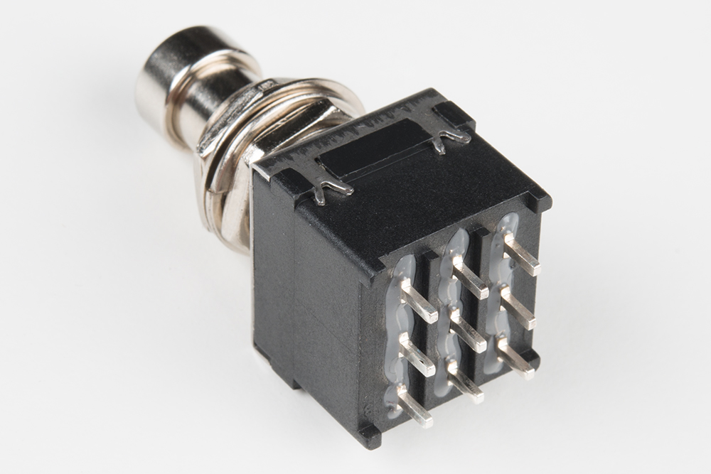
Inside the switch, there are actually three separate switches that actuate together when the button is pressed. This switch is actually designed specifically for guitar pedals.
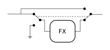
Through the years, a wide variety of bypass switching circuits have been used, many of which use a two-pole switch. The most usable configuration of a two pole switch uses both sections of the switch to steer the signal around the circuit in a "true bypass" configuration. When bypassed, the Proto Pedal passes signal even if the circuit isn't powered.

The protopedal uses a variant of true bypass switching. The input of the effect is tied to ground when the effect is bypassed, which keeps some high-gain circuits from misbehaving.
Indicator LED
In the discussion of bypass switching, we only used two of the three poles on the switch. The third section is used to switch the LED, showing the status of the pedal.
There are two options for LED indicators. By default, there is a surface mount red LED on the PCB, so you can tell the bypass status on your workbench. If you want to defeat this LED, remove the solder blob on SJ1.
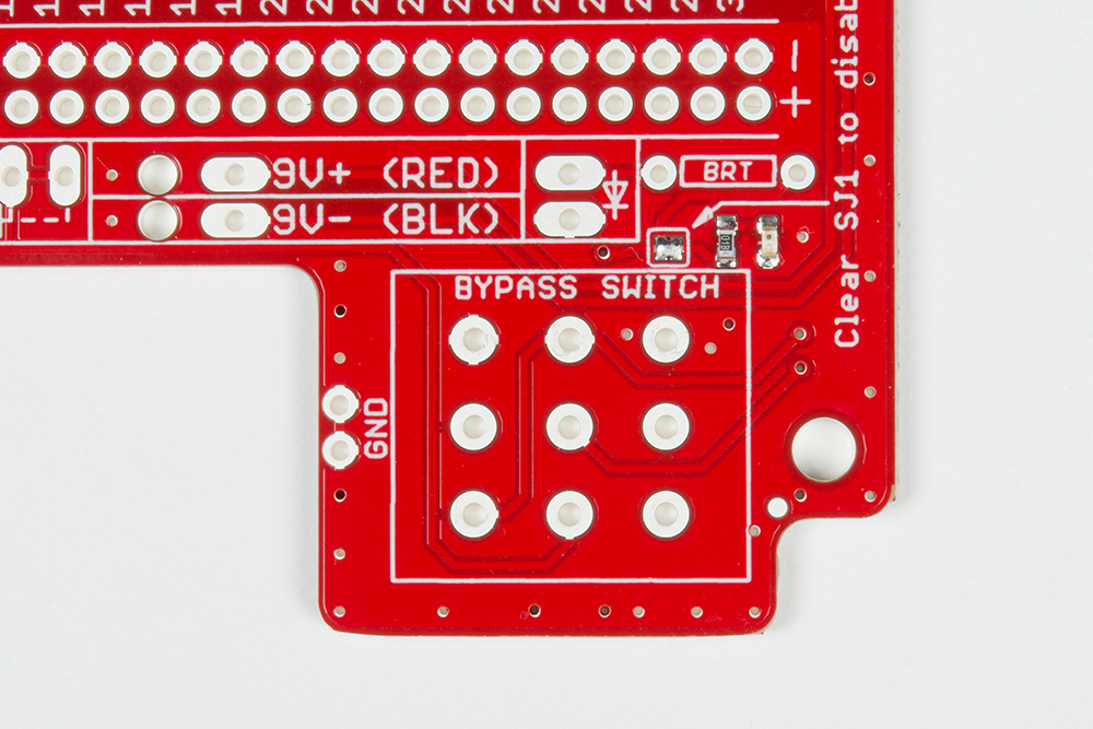
The second LED option allows for a through-hole 5mm LED near the footswitch, which aligns with the hole in the chassis. There is a through-hole bias resistor next door, marked BRT, so you can configure the brightness of the LED.
AC Coupling
Adding the Offset
Guitar signals generally swing about 0V, with an amplitude of around one volt, peak-to-peak (though this varies quite a bit with different pickups, string materials, and playing styles).
Pedal circuits are typically powered by a single 9V DC battery, which limits the signal swing to that range. The negative peaks of the signal fall below ground, which is outside the region where the circuits operate.
To aid this situation, an offset is added to the signal. This is called a "DC bias."
As you analyze pedal schematics, you'll learn to identify where this offset is generated. It's frequently a pair of equal-value resistors wired as a divider between 9V and ground, sometimes with a cap in parallel with the lower resistor. Let's look at an actual schematic and identify the offset voltage.

(Schematic courtesy Jack Orman, used with permission)
The offset voltage is produced by the divider formed by R8 and R9. The node where they meet will be one-half of V+ (4.5V if powered by a 9V battery).
In more complex schamatics, the half-rail voltage might be used multiple places in the circuit, and there might be more than one divider.
Coupling Capacitors
The DC bias voltage is required inside the circuit, but it needs to be prevented form reaching the outside world. If the DC bias finds its way to the bypass switch, it will cause pops or thumps when the switch is is actuated. Similarly, the guitar, amplifier, and other pedals are expecting the signal to be centered around 0 V. The bias is removed using capacitors on the effect input and output.
The the Super Buffer schematic above, the input coupling capacitor is C1 and the output coupling capacitor is the parallel combination of C2 and C3.
The Proto Pedal anticipates that circuits will need those caps, providing footprints for them on the edge near the battery.
The Proto Pedal also has 1 MΩ pulldown resistors on the external sides of the coupling caps, similar to the 2.2M Ω R5 and R7 in the buffer schematic. Some types of capacitors leak the bias voltage, slowly charging the external sides of the caps. The pull-down resistors keep the external sides of the caps at ground potential, preventing popping when the switch is actuated.
Wait, There's No Power Switch?
In the discussion of the stomp switch above, you'll notice the switch is being used to steer the signal through the effect, and turn the LED on and off. It's not actually turning the circuit on and off.
If you're familiar with guitar peals, you understand that the input jack needs to be connected for the pedal to come on. The input jack functions as the power switch!
Let's take a closer look at how this works, by looking at the components in question.
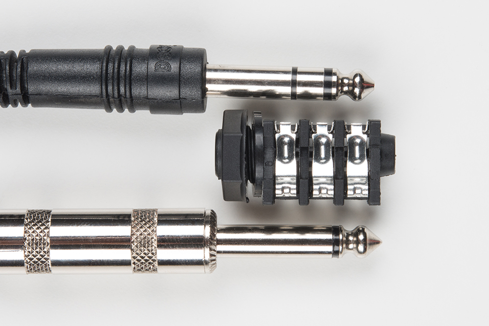
Here, from top to bottom, are
- A tip-ring-sleeve (TRS) 1/4" jack.
- A 1/4" TRS socket.
- A standard guitar cable with a tip-sleeve (TS) 1/4" jack.
The difference between the TS and TRS jacks is that the TRS jack has a third conductor (the ring) between the tip and sleeve. Or, seen from the opposite perspective, the TS jack is a TRS jack with the ring and sleeve shorted together.
The input on an effect pedal is actually a tip-ring-sleeve socket, with three conductors. When a TS cable is plugged into it, it bridges the ring to the sleeve. Pedals use that connection as a low-side power switch, connecting the negative terminal of the battery to the pedal ground.
If you've used pedals with 9V betteries, you quickly learned that you had to unplug them when you weren't using them if you didn't want the batteries to die.
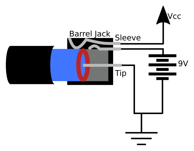
Power Input Selection
The Proto Pedal has two power sources: the barrel jack and the 9 volt battery snap. These connections are arranged so that when the barrel is plugged in, the battery is out of the circuit.
This relies on a somewhat obscure detail in the construction of the barrel jack: it has an extra, spring loaded, contact.
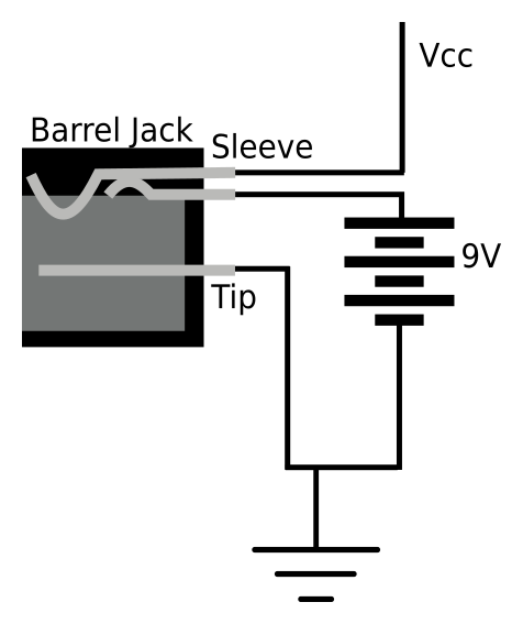
When nothing is plugged in, the spring holds the second and third contacts together. When the barrel is plugged in, the jack pushes the contacts apart, disconnecting the battery.
In the sophisticated world of pedalboard design, it's common that the battery is omitted entirely, and the pedals are powered by DC power supplies.
Finally, as we mentioned in the introduction, guitar pedals use a barrel jack polarity that's backwards from other disciplines. Just in case the wrong DC adapter finds its way into the picture, the power connections are protected using a P-channel MOSFET that will only conduct when forward biased. A reverse-polarity adapter (or fumbling a 9V battery against the snap) won't cause any damage - it simply won't work.
Some Notes on "Tone Suck"
Through the years, some guitar pedals have become notorious for introducing unwanted changes in the input signal. Perhaps they make the sound quieter, darker, the low end disappears, or just becomes somewhat indistinct -- sometimes even with the pedal bypassed!
Unlike some hard to prove audiophile concepts, "Tone Suck" is a real phenomena, which can be easily explained with a little engineering analysis.
An electric guitar pickup is a high impedance inductive source. If the load on that source is too high, it forms a frequency dependent voltage divider, and the high end disappears. Early in the pedal era, this fact wasn't fully recognized, and some circuits had unusually low input impedance.
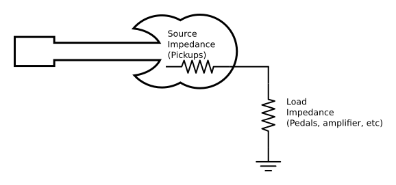
To prevent undue loading, the load impedance should be ten times the source impedance.
In round numbers, the source impedance of guitar pickups is commonly in the 10KΩ to 25KΩ range. To work well with both sources, a guitar input should have ten times that impedance, or 250K -- even higher, such as 1 MΩ, is better. Typical hi-fi and pro-audio inputs are in the 10KΩ to 47KΩ neighborhood. If a guitar is plugged directly into them, it probably loses some mojo.
There are two solutions to the impedance loading problem. The first is to design circuits with a suitably high input impedance. The second is to add a buffer stage in front of the low Z input. The buffer could be as simple as a JFET or MOSFET configured as a source follower, or even another pedal inserted between the guitar and the low impedance input.
The bypass circuitry in older pedals sometimes cut corners, as well. There have been switching strategies that use a single pole switch to simply select between the input signal or the effect output, so the effect is always loading the pickups, even when bypassed.

With a two pole stomp switch, the switch can steer the signal completely around the effect circuit, removing the load entirely.
Finally, the coupling capacitors in some pedals are simply too small, causing a loss of low end.
The Proto Pedal incorporates a number of features that should prevent these problems.
- The bypass switch is configured in a true-bypass configuration.
- The input impedance of the PCB is 1 MΩ -- high enough to not form an undue load on most guitars.
- The coupling capacitors on the input and output are user-selectable, so they can be chosen to prevent low-end loss.
Resources and Going Further
This guide is the first of several for the Proto Pdeal. Where you go next depends on your interests and background.
- If you're interested in analog circuitry, check out the analog EQ pedal example project.
- If you're more familiar with writing software and want to design affects by writing programs, check out the programmable digital pedal example.
Resources
- The barrel-jack polarity protection circuit is commonly found in automotive electronics. One applicable reference is this TI Application Report
- We carry 5mm LEDs in many different colors.
- We offer 10K Audio Taper Pots and 10K Linear Taper Pots
- We also have several types of knobs
- Gray Aluminum for splined shaft pots.
- Black Aluminum for splined shaft pots.
- Black stove-type with set-screw for 1/4" diameter shaft.
- Black chickenhead with set-screw for 1/4" diameter shaft.
- Resistor assortment
- Capacitor assortment
- Discrete semiconductor assortment
- Stranded and solid hookup wire.
Going Further
- Nic Collins' Handmade Electronic Music book contains a number of circuit snippets that could make useful pedals.
- Craig Anderton's Electronic Projects for Musicians book is a great jumping-off point for learning about pedals and musical electronics.
- There are many pedal construction websites around, including Geofex, AMZ, and Aron Nelson's DIY Stompboxes.