Proto Pedal Example: Analog Equalizer Project
 Byron J.
Introduction
Having assembled the Proto Pedal in the Proto Pedal Assembly Guide, we'd like to continue by actually building an effect circuit on the board. The circuit we'll be basing this on is Fred Forssell's swinging-input equalizer.
Required Materials
To build the EQ circuit, we'll need to following components:
Tools
You'll also need the usual tools to solder things together.
- Soldering Iron
- Lead-based or Lead-free solder
- Diagonal or Flush cutters
- Wire Strippers
Additionally, while it's not required, we were using a Resistor Lead Forming tool to get the resistors bent to precise lengths.
Suggested Reading
- If you're here, we'll assume that you're familiar with the Proto Pedal Assembly and Theory guide. If not, you should start there.
- In parallel with this guide, you might also be interested in some information abouyt preparing the Proto Pedal chassis.
- This project is based on Fred Forssell's Equalizer Whitepaper, in particular his Equal Resistor Gyrator.
The Circuit
The Challenge - to devise an analog circuit that makes a usable guitar pedal and can be built entirely from parts in the SparkFun catalog.
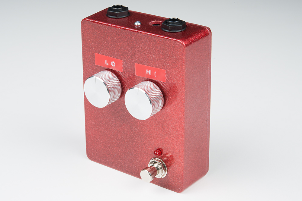
The Result - an analog equalizer based on Fred Forssell's equalizer white paper. The result is a good sounding and flexible pedal design, featuring bell-shaped bass and treble controls. The low frequency is centered on 100 Hz, and the high frequency is centered on 3.2 kHz. Each band offers about 10 dB cut and boost.
(click to enlarge).
The filters are also easily tuned to other frequencies and modified for shelving response.
(click to enlarge).
Assembly
Step Zero
To begin, we'll assume that you've completed the basic assembly of the proto pedal board.
If you're using the Proto Pedal Chassis, you'll need to prepare it by drilling holes for two potentiometers, as shown in the Chassis Hookup Guide.
With the prerequisites complete, you can start the sequence below. We're going to be stepping in fairly large chunks. Each step lists the required components, so you can prepare them before you commence. Once they have been placed, double-check your solder joints, and compare your work to the photos.
Playing Battleship
In the following steps, we're going to use the grid notation seen on a standard solderless breadboard. From left to right, the columns are numbered 1 to 30, and, from bottom to top, the rows are assigned letters from A through J. Any hole in the center of the board can be referenced by number-letter coordinate, such as 27L or 7G.
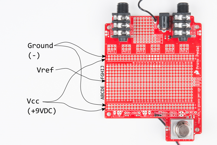
Additionally, we'll be using the power and center rails of the proto area. At the top and bottom edge of the board are 9V power (AKA Vcc) on the traces marked + and ground on the traces marked -. One of the center traces is used as a half-rail bias voltage, which we'll refer to as Vref.
In the following steps, we'll give the coordinate designation of each component.
Step One: Wire Jumpers
The first step is to use solid core hookup wire, and make some basic connections between sets of pads in the proto area. For clarity, we're using many different colors of wire, but not using any red wire.
| Jumper Number | Color | Start Coordinate | End Coordinate |
|---|---|---|---|
| 1 | Black | In | 1A |
| 2 | Yellow | 2A | Lower Vcc |
| 3 | Blue | 3E | 3F |
| 4 | Green | 10J | Upper Ground |
| 5 | Yellow | 11J | Pot3 Left |
| 6 | Black | 12J | Pot3 Right |
| 7 | Blue | 17J | Pot3 Middle |
| 8 | White | 18E | Pot4 Middle |
| 9 | Green | 20J | Upper Ground |
| 10 | Bare | 11D | 12D |
| 11 | Yellow | 12C | Vref |
| 12 | Yellow | 13A | Lower Vcc |
| 13 | Black | 16F | Out |
| 14 | Bare | 22G | 23G |
| 15 | Bare | 21D | 22D |
| 16 | Yellow | 23A | Lower Vcc |
Installed, these jumpers look like this.
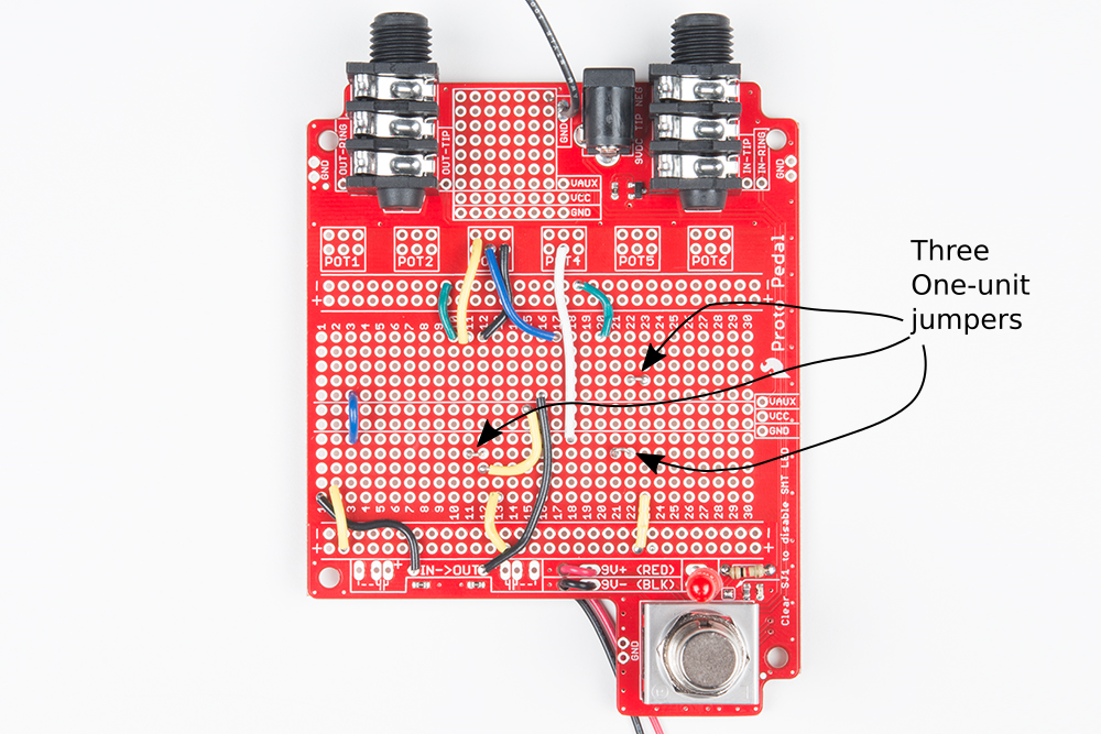
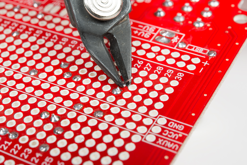
The jumpers are soldered to the back of the board and trimmed close to the board. If the tails stick out too far, they will short to the metal enclosure.
When you're done, count the number of jumpers -- there should be sixteen in total. If you find that you're short, doublecheck that you've got the 0.1 inch wire links as noted in the photo.
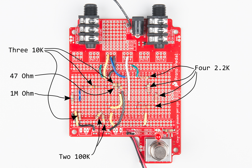
Step Two: Resistors
There are eleven resistors in this design. To get started, select the following from your resistor assortment. We include the color markings below. The packaging of the resistor assortment serves as an illustrated guide.
| Resistor Value | Value Color Code | Start Coordinate | End Coordinate | Placement Notes |
|---|---|---|---|---|
| 1M Ω | brown-black-green-gold | 1D | Vref | |
| 10K Ω | brown-black-orange-gold | 3B | Lower Ground | |
| 10K Ω | brown-black-orange-gold | 4G | 11G | 0.7" long |
| 10K Ω | brown-black-orange-gold | 12H | 16H | 0.4" long |
| 100K Ω | brown-black-yellow-gold | 10A | Lower Vcc | |
| 100K Ω | brown-black-yellow-gold | 10B | Lower Ground | At angle |
| 47 Ω | yellow-violet-black-gold | 13G | 16G | |
| 2.2K Ω | red-red-red-gold | 21J | 24J | |
| 2.2K Ω | red-red-red-gold | 24H | Vref | |
| 2.2K Ω | red-red-red-gold | 26D | Vref | |
| 2.2K Ω | red-red-red-gold | 20C | 26C | 0.6" long |
These resistors get installed as shown below. Take note of a couple placement details: some of the resistors are stretched longer than you might expect, and one of the 100K Ω resistors is at an angle.
Step Three: Capacitors
There are ten capacitors, as follows. The values are printed on the caps, and there is a value decoder on the package. The ceramic caps are the small yellow ones, and the electrolytic caps are small black cylinders.
| Capacitor Value | Value Marking | Start Coordinate | End Coordinate | Orientation Notes |
|---|---|---|---|---|
| 100 pf ceramic | 101 | 12I | 16I | |
| 0.01 uf ceramic | 103 | 18A | 20A | |
| 0.1 uf ceramic | 104 | Input Coupling | ||
| 0.1 uf ceramic | 104 | 22B | 24B | |
| 0.1 uf ceramic | 104 | 24A | 26A | |
| 1 uf electrolytic | 1uf/50V | 17G | 19G | `-` to right |
| 1 uf electrolytic | 1uf/50V | 22I | 24I | `-` to left |
| 1 uf electrolytic | 1uf/50V | 19I | 21I | `-` to left |
| 10 uf electrolytic | 10uf/25V | Output Coupling | `-` to right | |
| 10 uf electrolytic | 10uf/25V | 3H | 4H | `-` to right |
These capacitors are installed as shown below. We've noted the polarity orientation of the electrolytic caps above, also -- the body of the cap has a white stripe with "-" symbols printed to mark the negative leg.

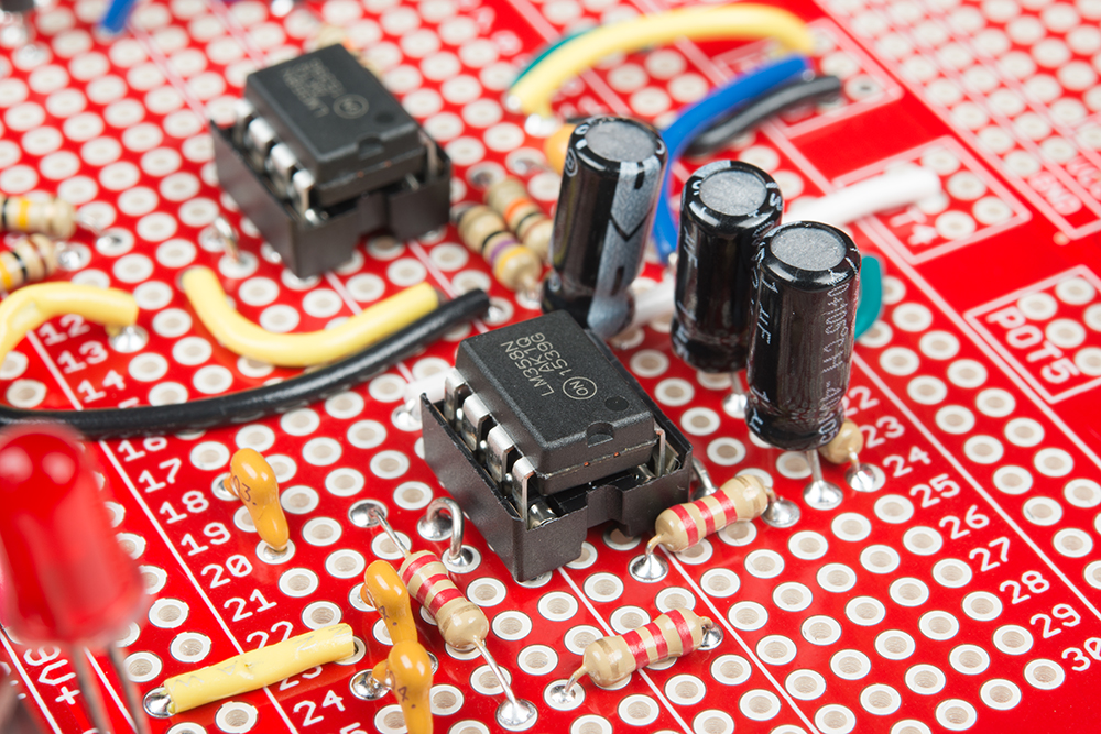
Step Four: Semiconductors
There are two types of semiconductor devices used in this project. The MOSFET is part of the Discrete Semiconductor Kit.
| Component | Marking | Start Coordinate | End Coordinate | Orientation Notes |
|---|---|---|---|---|
| 5LN01SP MOSFET | YB | 3C | 1C | Pin1 in column 3 YB facing upwards rounded edges facing downwards |
| DIP-8 IC Socket for LM358 | Row 10 | Row 13 | Spanning center trough Notch facing right | |
| DIP-8 IC Socket for LM358 | Row 20 | Row 23 | Spanning center trough Notch facing right |

Step Five: Flying Wires & Pots
This last step involves adding the pots to the board. We'll make a little subassembly out of them, then solder that to the PCB.
Because it needs to flex a bit, we're using stranded wire for this step. Cut the following pieces
| Length (Inches) | Lentgh (Metric) | Color |
|---|---|---|
| 2.5" | 5cm | Blue |
| 2.5" | 5cm | Red |
| 2.5" | 5cm | Blue |
| 5" | 13cm | Red |
| 5" | 13cm | Yellow |
| 5" | 13cm | Green |
First, orient the pots so the legs are facing the same direction. If you're using the enclosure, you can put the pots in the chassis holes to hold them in place while you work.
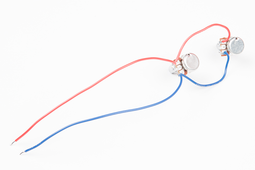
Use the shorter pieces of red wire to jump from pin 1 of the first pot to pin 1 of the second pot. Before soldering tie the longer piece of red wire to pin 1 of the first pot. Then, repeat the above, bridging from pin 3 to pin 3 with blue wire.
Next, solder the yellow wire to pin 2 of the first pot, and green wire to pin 2 of the other pot. The pot with the yellow wire is the low frequency control, and the pot with the green wire is the high frequency control.
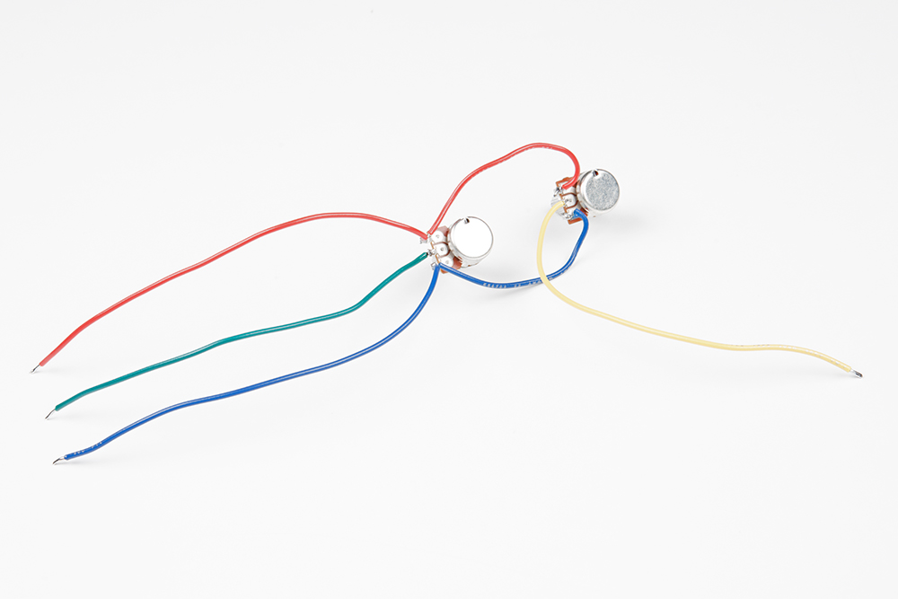
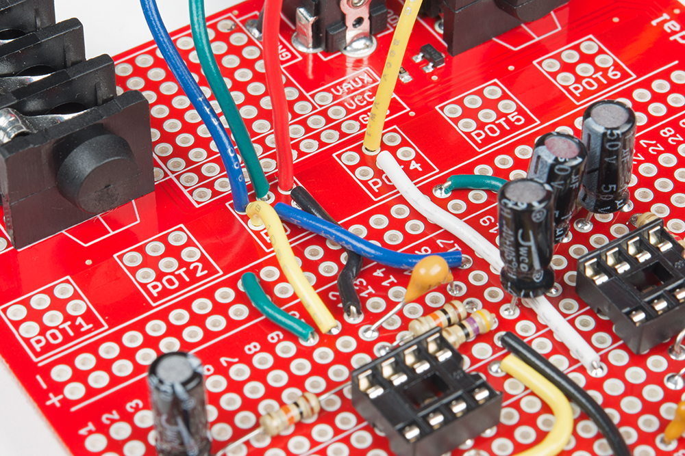
At this point, you'll have four wires trailing from the subassembly. They meet the PCB as shown below, in the pot 3 and 4 areas.
Last Step: Insert the ICs
With the above steps completed, you can insert the IC's in the sockets, taking care to align the pin-1 marks. The dimple should be at the top-right corner, and the notch should be facing right. The legs come splayed out a little bit wider than the sockets -- they'll need to be bent in a little bit to fit.
Now we can move on to testing the pedal!
Testing
Preparation
We'll start testing with a handful of sanity checks, or the proverbial "smoke test".
- Start by connecting power, either a 9V battery, or an external supply.
- Then connect a TS jack to the input. Recall that the input jack also serves as a hidden power switch, which is required to get the circuit to power up.
- Quickly and carefully feel the ICs and MOSFET. They should be cool to the touch. If not, power down and doublecheck your work.
- If they're getting warm, doublecheck that the ICs are oriented correctly, and that there aren't any solder bridges between adjacent fillets.
- Press the stomp switch a couple of times. The LED should toggle on and off with each actuation. The circuit is active when the LED is on, and bypassed when the LED is off.
- If you're using a bench supply with a built in ammeter, check that the current draw isn't excessive. On our bench, the device drew miniscule current when bypassed, and about 7 mA when switched to active.
Knowing the Controls
Since they're just flying on the ends of the wiring harness, it can be hard to tell which potentiometer is which. The pot with the yellow wire is the low frequency control, and the pot with the green wire is the high frequency control.
Before moving on to the next step, make sure that the pedal is active, the LED is on, and set both pots to the center of their rotation.
Operational Testing
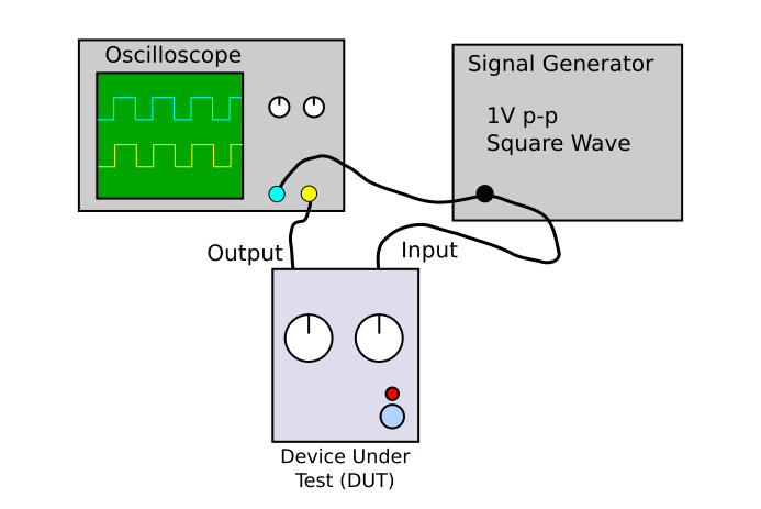
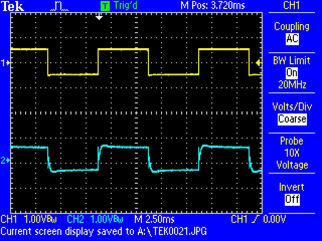
If you've got a function generator and oscilloscope, you can quickly test an EQ using a low frequency square wave.
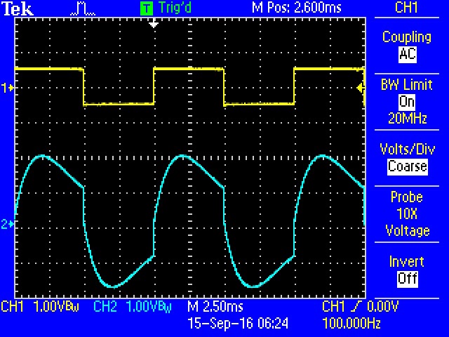
Connect the signal generator to the input, and set it for 100 Hz at 1 Vpeak-to-peak. You can view the output by connecting to the output tip test point, adjacent to the output jack. We'll be using a two-channel oscilloscope, with the first channel, in yellow, observing the signal generator output and the second channel, in blue, scoping the output of the EQ.
With both controls centered, the output will be very close to in input.
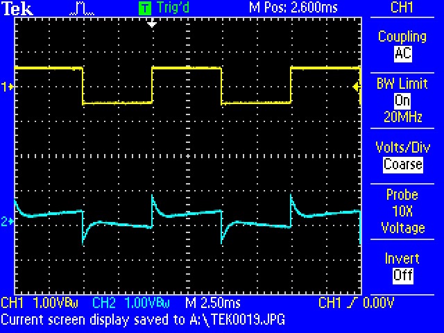
We'll first check the low frequencies. As you rotate the knob, the plateaus of the square wave will bend. Rotating the control colckwise increases the low frequency content, and the plateaus bend outward.
Rotating the control counter-clockwise bends the plateaus inward.
As you adjust the high frequencies, it becomes apparent just past the rising and falling edges of the square. When the high frequencies are rotated clockwise, the boost causes the edges to ring and overshoot.
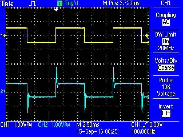
A cut causes a rounded second edge to appear near the vertical segments.
Failsafe
If you don't have a signal generator and oscilloscope availabile, there's no harm in just plugging the pedal in and listening to it. It's wise to perform the smoke test listed above first, and keep the master volume low until you're confident that the EQ is well behaved.
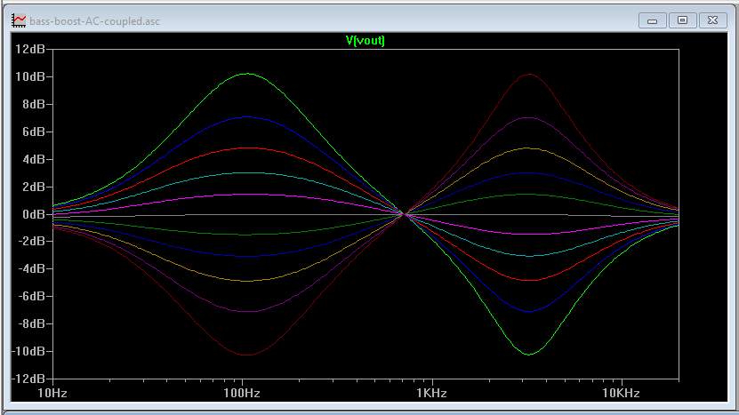
Performance
The frequency response is illustrated below, showing the effect of turning the potentiometers from their lowest to highest settings.
Seal It Up
If your testing yields satisfactory results, you're done!

You can put the pots through the enclosure, stick on knobs, and deploy the pedal for use!
In Use
This circuit performs best when the input signal isn't too hot. It's OK with a 1 Vpeak-to-peak input, but much above that and it distorts a bit (part of our testing involved a bass guitar with a high-output pickup that could easily produce 4 Vpp!). If you don't like the distortion, there are several potential fixes, listed below in order of increasing required effort.
- Turn down the volume a bit.
- Swap out the LM358 op-amps for better ones. We had success with NE5532's, at the cost of much higher quiescent current consumption.
- Increase the power supply voltage. Some pedal supplies offer an 18V output, or you can use two 9V batteries in series.
- Dig deeper into the design to add an attenuator on the input, with makeup gain on the output.
Theory
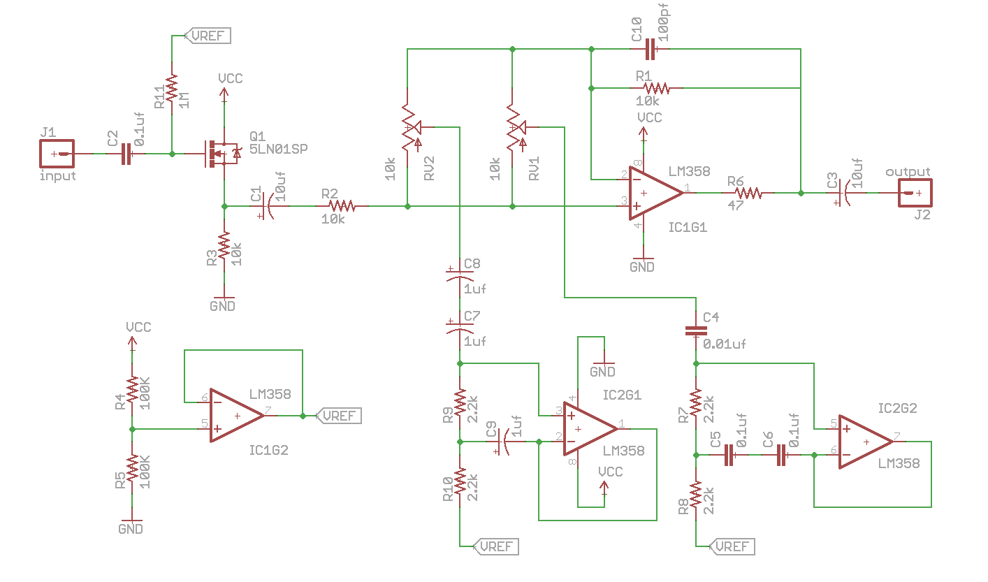
The schematic breaks down into several functional blocks.
We're going to quickly cover them below. If you want much more detail, you can find it in this white paper.
Input Buffer
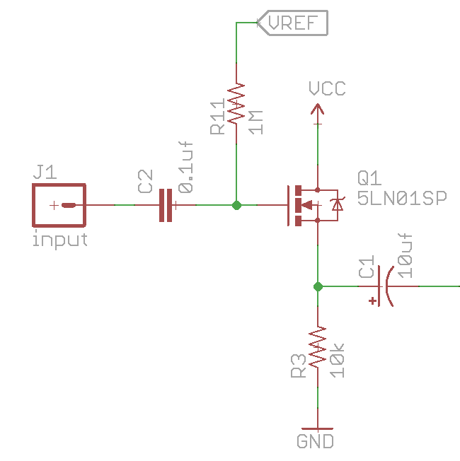
The start of our path through the equalizer is a single MOSFET, wired as a source follower. This bumps up the input impedance and prevents a loss of high frequencies when the pedal is switched on.
Because the input impedance is so high (defined by the parallel combination of R11 and the 1M input pull-down on the board, or 500 kΩ), the input coupling cap (C2) can be a very small value.
The buffer feeds into the...
Cut/Boost Amplifier
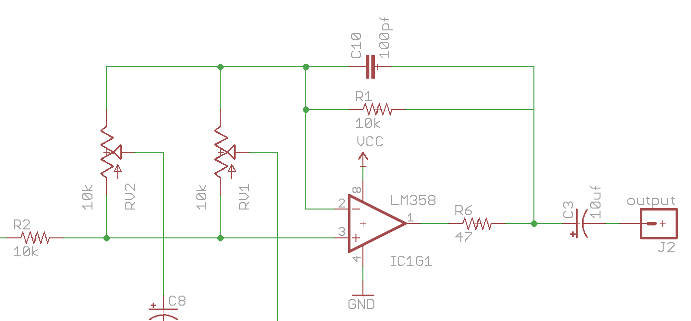
This amplifier is the heart of the equalizer circuit. It's configured as a unity gain noninverting amplifier. The gyrator circuits (more below!) are attached to potentiometers that "swing" between the inverting and non-inverting inputs of this op-amp. This EQ curcuit is sometimes called the "swinging input" topology.
Gyrators
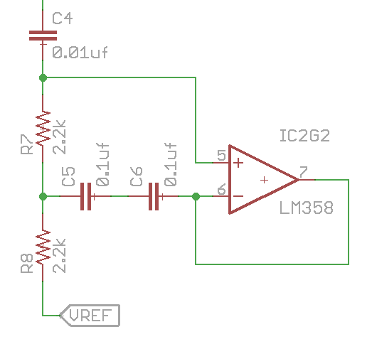
A gyrator is a virtual inductor, made with a capacitor and an op-amp. By putting a second capacitor in series with the gyrator, a band-stop filter is created.
Since we're using the decade-value capacitors from the capacitor kit, we're taking advantage of the series combination of some of the caps to get different values, as implemented with C7-C8 and C5-C6.
These band stop filters are attached to potentiometers that move them between the inverting and non-inverting inputs of the cut/boost amplifier.
When the bandstop filter is on the + input, that band is removed from the input signal, resulting in a cut. When it's on the - input, it's removing the frequency from the feedback path. The result of cutting the feedback is a boost at the frequency. When the potentiometers are in the middle, the cut and boost actions balance each other, with no net change.
Buffered Half-Rail
Finally, part of the circuit serves as an ancillary power supply.
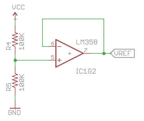
The circuit requires three op-amps, but with two dual op-amp chips, we have a spare. That extra amplifier is configured as a voltage follower on a half-rail voltage. It's used for the DC bias added to the signal and also as the "virtual ground" that the gyrators dump signal into.
Many pedals use pairs of equal value resistors as dividers, to create Vcc/2 reference voltages. By buffering a single divider with an op-amp, we have a half-rail of lower impedance. It costs an op-amp stage (that was otherwise unused) but probably saves a number of resistors.
The half rail is treated as VAUX, applied to one of the lateral traces in the center of the breadboard.
Resources and Going Further
Resources
- The basis for this project was Fred Forssell's Equalizer design.
- The basis for the design is explored in his EQ whitepaper
- There is a secondary document that contains detailed information on the gyrator math.
- The National Semiconductor Audio Radio Handbook contains a similar gyrator EQ circuit. The gyrators are slightly different, and their explanation is much more math-heavy.
- If you're really interested in EQ circuits, Douglas Self's Small Signal Audio Design is a great reference.
Going Further
Modifications
The filters in the circuit are highly configurable. By adjusting the component values, the center frequencies can be moved, bandwidths adjusted, and the maximum amount cut and boost altered. The gyrator paper mentioned above covers the basics.
For bass guitar, simply doubling the values of the gyrator capacitors (C4, C5, C6, C7, C8 and C9) will drop the bands by an octave.
If you'd like to simulate different component values, there is an LT SPICE simulation in the Github repository.
Try other capacitor chemistries, too. Again, the design challenge was to design something using only parts in stock at SparkFun. If you've got a stash of fancier caps, this is a great circuit to try them in. Polyester film (Mylar) caps work nicely in audio circuits, and silver-mica caps are also highly regarded.
As mentioned in the testing section, the LM358 op-amps have been surpassed by newer ones. They share a footprint with many other dual op-amps.
Finallly, if you're really ambitious, and can add more frequency bands by duplicating the potentiometer-gyrator stages. The heart of this circuit is the basis for a multi-band graphic equalizer.