MPU-9150 Hookup Guide
 .Brent.
Hardware Overview
The Pinout
In total, the MPU-9150 Breakout breaks out 11 pins.

The bare-minimum connections required are broken out on the left side of the board. These are the power and I2C pins (the communication interface the board defaults to):
| Pin Label | Pin Function | Notes |
|---|---|---|
| GND | Ground | 0V voltage supply |
| VCC | Power Supply | Supply voltage to the chip. Should be regulated between 2.375V and 3.465V. |
| SDA | I2C: Serial Data | I2C: Serial data (bi-directional) |
| SCL | Serial Clock | I2C serial clock (up to 400kHz) |
The remaining pins break out additional functionality and interrupt outputs:
| Pin Label | Pin Function | Notes |
|---|---|---|
| ESD | Auxiliary I2C master serial data | 9150 can act as a master or pass-through to additional I2C devices. |
| ESC | Auxiliary I2C master serial clock | 9150 can act as a master or pass-through to additional I2C devices. |
| COUT | Clock output | Outputs a 50% duty cycle square wave (see register map). |
| CIN | Clock input | Optional external reference clock input, grounded through jumper. I using an external clock source, cut 'CLK' jumper. |
| AD0 | I2C Slave Address LSB | If low I2C address is 0x68, else 0x69. Connected to jumper. (0x68 default) |
| FSYNC | Frame synchronization | External frame sync input that latches to capture external bus interrupts If using this pin cut 'SYNC' jumper. |
| INT | Interrupt pin | Configurable digital output to signal the host processor of an event. |
Power Supply
The VCC and GND pins are where you'll supply a voltage and 0V reference to the IC. The breakout board does not regulate this voltage, so make sure it falls within the allowed supply voltage range of the MPU-9150: 2.375V to 3.465V. Logic voltage levels can be as low as 1.8V ±5% up to VCC.
The communication pins are not 5V tolerant, so they'll need to be regulated to within a few mV of VDD.
Communication
SDA, SCL, ESD, and ESC are used for the I2C interfaces. The auxiliary clock and data pins will require external pull-up resistors. These ave to be tuned on a case-by-case basis depending on bus capacitance to get proper rise times.
SDA and SCL have integrated 10KΩ pull-ups. If you plan on using more than one I2C device on the bus, you might want to remove these pull-ups. If the I2C lines are pulled-up too strongly by multiple sets of pull-ups, the bus will likely be out of spec and not function correctly.
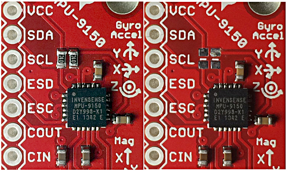
The following image shows a stock PCBA on the left, and one with the pull-up resistors removed on the right. To remove these, I recommend reflowing a fair amount of solder onto the resistors. It doens't take very long to fully cover all 4 joints with molten solder and the two part will slide right off. So easily in my case that I wasn't able to capture a picture of the excess solder before the parts had come off. Wick off the excess solder, wipe clean with some DI water, and you are done.
Interrupts
There are a variety of interrupts on the MPU-9150. While connecting up to these is not as critical as the communication or power supply pins, using them will help you get the most out of the chip. The INT pin is a digital output to the host controller. The FSYNC pin can be configured as an interrupt input to optionally be passed through out the INT pin.
These can be programmed to interrupt as either active-high or active-low. More details on these configurations can be found in the product register map.
The Jumpers
The most commonly used jumper will be to the address pin (AD0). It defaults to being pulled to ground selecting address 0x68, but with a soldering iron can be changed to be pulled up, switching the I2C address to 0x69.
The intention of these jumpers is to make it as easy-as-possible to use the board; using as few wires as possible. The CLK jumper is used to ground the external clock input as the datasheet recommends when not using an external clock. Make sure to cut this jumper if you attach an external clock to the CIN connection. The SYNC jumper ties FSYNC to ground as the manufacturer instructs one to do when not using it. Make sure to cut this jumper if use the FSYNC through hole connection.

To disable any of these jumpers, whip out your handy hobby knife, and carefully cut the small traces between middle pad and edge pads.
Funny Business
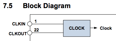
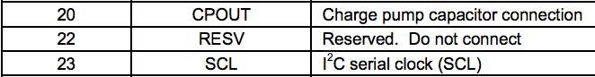
Be very careful trusting the datasheet. It's full of inconsistencies or lacking clarification. For example pin 22. There is a single reference to it functioning as a clock output (next image). There are several places stating that it's not to be used, such as the table shown two images below.
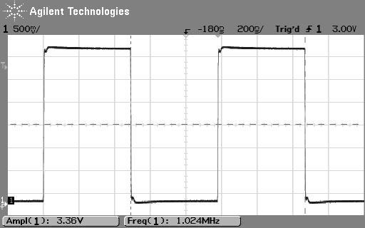
The register map reads "This bit also enables the clock output.", but that's the only reference. It's not even specified clearly to which bit they are referring. We were able to test this, and sure enough it outputs a clock. Maybe this clock is is okay to use. Maybe it was designed for factory testing only.
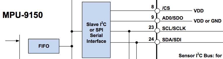
SPI is another example of being poorly documented. The following image implies that the address selection line is also SDO. The digital IO power supply pin is also the chip select line. Most serial peripherals we are familiar with don't source power out their chip select pins.
Finally one last quote to show how amazing the datasheet is: "The internal registers and memory of the MPU-9150 can be accessed using either I2C at 400 kHz." Either fast mode I2C, or what? As often as we tell you to RTFM, sometimes the manual can be misleading.