MicroMod mikroBUS™ Carrier Board Hookup Guide
Hardware Overview
Board Dimensions
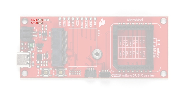
The MicroMod mikroBUS™ carrier board dimensions are approximately 3.35" x 1.40" with four mounting holes compatible with 4-40 screws or standoffs.
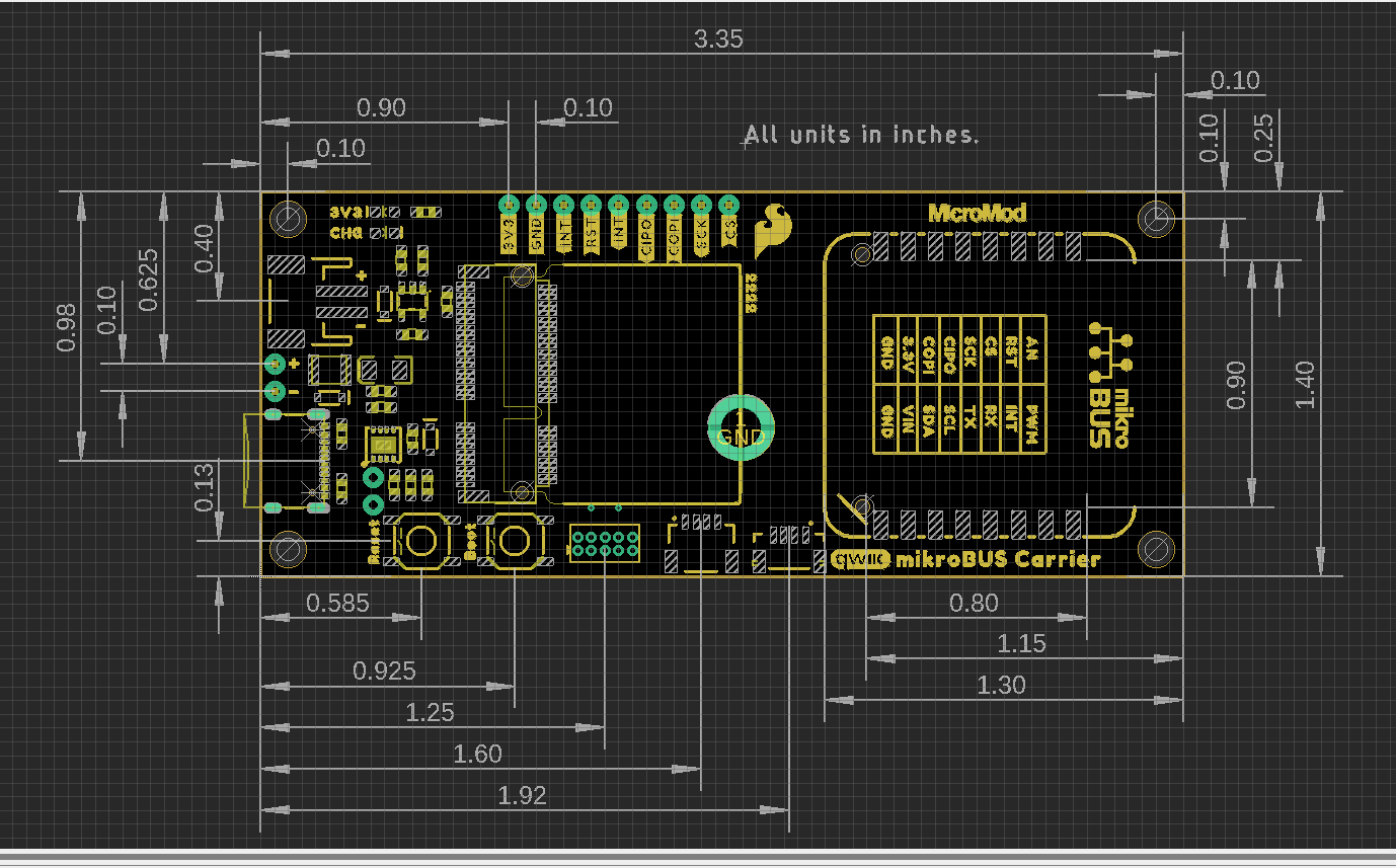
The board also includes a mikroBUS™ socket for MikroElektronika's Click boards™.
Common Components
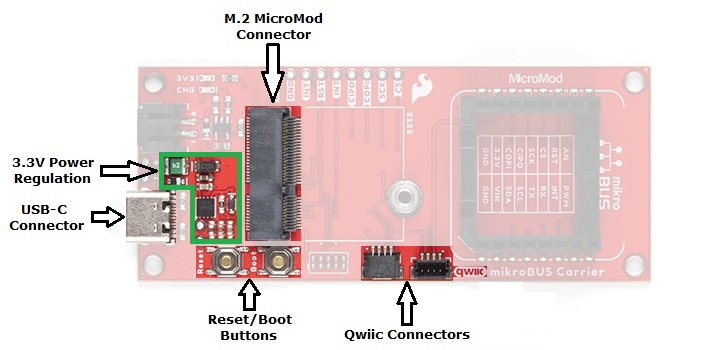
Most SparkFun MicroMod Carrier Boards will have some common components and all MicroMod Carrier Boards will have the keyed M.2 MicroMod connector for a Processor board. The photo and list below outline the common components between the mikroBUS™ carrier board and other MicroMod Carrier Boards.
- M.2 MicroMod Connector - This special keyed M.2 connector lets you install your MicroMod Processor of choice to the mikroBUS Carrier Board.
- USB-C Connector - Connect to your computer to program your processor and provide power to the board.
- 3.3V Regulator - Provides a regulated 3.3V and sources up to 1A.
- Qwiic Connectors - The standard Qwiic connectors to connect other Qwiic devices for your MicroMod project.
- Boot/Reset Buttons - Push buttons to enter boot mode on processors and to reset your MicroMod circuit.
Battery Charger
The board also has a MCP73831 Single-Cell Lithium-Ion/Lithium-Polymer Charge IC so you can charge an attached single-cell LiPo battery. The charge IC receives power from the USB connection and can source up to 450mA to charge an attached battery.
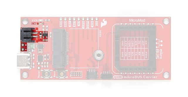
Status LEDs
The carrier board has two status LEDs:
- 3V3 - This LED indicates when 3.3V power is available top the board.
- CHG - This LED indicates the status of the charging circuit operation.
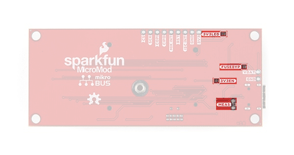
Solder Jumpers
There are four adjustable solder jumpers on the mikroBUS™ carrier board labeled MEAS, BYP, 3.3V_VE and 3.3V. The table below briefly outlines their functionalities:
| Jumper Name/Label | Description | Default State |
|---|---|---|
| Measure/MEAS | Open this jumper to probe the current draw at the 3.3V output of the regulator. For help measuring current, take a look at our How to Use a Multimeter tutorial. | CLOSED |
| Bypass/BYP | The "penny-in-the-fuse" jumper. Bypasses the 6V/2A fuse and nets VIN and V_USB together. Close only if you know what you are doing! | OPEN |
| Voltage Regulator Enable/VE | Voltage regulator control. Close this jumper to control the VREG in low-power applications. | OPEN |
| 3.3V LED Power/3V3 LED | Connects the 3.3V LED to 3.3V via a 1K Ohm resistor. Open to disable the LED. | CLOSED |
MicroMod Pinout
Since this carrier board is designed to work with all of the MicroMod Processors we've included the table below to outline which pins are used so, if you would like, you can compare them to the pinout tables in their respective Hookup Guides.
| AUDIO | UART | GPIO/BUS | I2C | SDIO | SPI | Dedicated |
| Function | Bottom Pin |
Top Pin |
Function | ||||||
|---|---|---|---|---|---|---|---|---|---|
| (Not Connected) | 75 | GND | |||||||
| 3.3V | 74 | 73 | G5 / BUS5 | ||||||
| RTC_3V_BATT | 72 | 71 | G6 / BUS6 | ||||||
| SPI_CS1# | SDIO_DATA3 (I/O) | 70 | 69 | G7 / BUS7 | |||||
| SDIO_DATA2 (I/O) | 68 | 67 | G8 | ||||||
| SDIO_DATA1 (I/O) | 66 | 65 | G9 | ADC_D- | CAM_HSYNC | ||||
| SPI_CIPO1 | SDIO_DATA0 (I/O) | 64 | 63 | G10 | ADC_D+ | CAM_VSYNC | |||
| SPI COPI1 | SDIO_CMD (I/O) | 62 | 61 | SPI_CIPO (I) | |||||
| SPI SCK1 | SDIO_SCK (O) | 60 | 59 | SPI_COPI (O) | LED_DAT | ||||
| AUD_MCLK (O) | 58 | 57 | SPI_SCK (O) | LED_CLK | |||||
| CAM_MCLK | PCM_OUT | I2S_OUT | AUD_OUT | 56 | 55 | SPI_CS# | |||
| CAM_PCLK | PCM_IN | I2S_IN | AUD_IN | 54 | 53 | I2C_SCL1 (I/O) | |||
| PDM_DATA | PCM_SYNC | I2S_WS | AUD_LRCLK | 52 | 51 | I2C_SDA1 (I/O) | |||
| PDM_CLK | PCM_CLK | I2S_SCK | AUD_BCLK | 50 | 49 | BATT_VIN / 3 (I - ADC) (0 to 3.3V) | |||
| G4 / BUS4 | 48 | 47 | PWM1 | ||||||
| G3 / BUS3 | 46 | 45 | GND | ||||||
| G2 / BUS2 | 44 | 43 | CAN_TX | ||||||
| G1 / BUS1 | 42 | 41 | CAN_RX | ||||||
| G0 / BUS0 | 40 | 39 | GND | ||||||
| A1 | 38 | 37 | USBHOST_D- | ||||||
| GND | 36 | 35 | USBHOST_D+ | ||||||
| A0 | 34 | 33 | GND | ||||||
| PWM0 | 32 | 31 | Module Key | ||||||
| Module Key | 30 | 29 | Module Key | ||||||
| Module Key | 28 | 27 | Module Key | ||||||
| Module Key | 26 | 25 | Module Key | ||||||
| Module Key | 24 | 23 | SWDIO | ||||||
| UART_TX2 (O) | 22 | 21 | SWDCK | ||||||
| UART_RX2 (I) | 20 | 19 | UART_RX1 (I) | ||||||
| CAM_TRIG | D1 | 18 | 17 | UART_TX1 (0) | |||||
| I2C_INT# | 16 | 15 | UART_CTS1 (I) | ||||||
| I2C_SCL (I/0) | 14 | 13 | UART_RTS1 (O) | ||||||
| I2C_SDA (I/0) | 12 | 11 | BOOT (I - Open Drain) | ||||||
| D0 | 10 | 9 | USB_VIN | ||||||
| SWO | G11 | 8 | 7 | GND | |||||
| RESET# (I - Open Drain) | 6 | 5 | USB_D- | ||||||
| 3.3V_EN | 4 | 3 | USB_D+ | ||||||
| 3.3V | 2 | 1 | GND | ||||||
| Signal Group | Signal | I/O | Description | Voltage | Power | 3.3V | I | 3.3V Source | 3.3V |
|---|---|---|---|---|
| GND | Return current path | 0V | ||
| USB_VIN | I |
USB VIN compliant to USB 2.0 specification. Connect to pins on Processor Board that require 5V for USB functionality. |
4.8-5.2V | |
| RTC_3V_BATT | I |
3V provided by external coin cell or mini battery. Max draw = 100μA. Connect to pins maintaining an RTC during power loss. Can be left NC. |
3V | |
| 3.3V_EN | O | Controls the carrier board's main voltage regulator. Voltage above 1V will enable 3.3V power path. | 3.3V | |
| BATT_VIN/3 | I |
Carrier board raw voltage over 3. 1/3 resistor divider is implemented on carrier board. Amplify the analog signal as needed for full 0-3.3V range |
3.3V | |
| Reset | Reset | I | Input to processor. Open drain with pullup on processor board. Pulling low resets processor. | 3.3V |
| Boot | I | Input to processor. Open drain with pullup on processor board. Pulling low puts processor into special boot mode. Can be left NC. | 3.3V | |
| USB | USB_D± | I/O | USB Data ±. Differential serial data interface compliant to USB 2.0 specification. If UART is required for programming, USB± must be routed to a USB-to-serial conversion IC on the processor board. | |
| USB Host | USBHOST_D± | I/O | For processors that support USB Host Mode. USB Data±. Differential serial data interface compliant to USB 2.0 specification. Can be left NC. | |
| CAN | CAN_RX | I | CAN Bus receive data. | 3.3V |
| CAN_TX | O | CAN Bus transmit data. | 3.3V | |
| UART | UART_RX1 | I | UART receive data. | 3.3V |
| UART_TX1 | O | UART transmit data. | 3.3V | |
| UART_RTS1 | O | UART request to send. | 3.3V | |
| UART_CTS1 | I | UART clear to send. | 3.3V | |
| UART_RX2 | I | 2nd UART receive data. | 3.3V | |
| UART_TX2 | O | 2nd UART transmit data. | 3.3V | |
| I2C | I2C_SCL | I/O | I2C clock. Open drain with pullup on carrier board. | 3.3V |
| I2C_SDA | I/O | I2C data. Open drain with pullup on carrier board | 3.3V | |
| I2C_INT# | I | Interrupt notification from carrier board to processor. Open drain with pullup on carrier board. Active LOW | 3.3V | |
| I2C_SCL1 | I/O | 2nd I2C clock. Open drain with pullup on carrier board. | 3.3V | |
| I2C_SDA1 | I/O | 2nd I2C data. Open drain with pullup on carrier board. | 3.3V | |
| SPI | SPI_COPI | O | SPI Controller Output/Peripheral Input. | 3.3V |
| SPI_CIPO | I | SPI Controller Input/Peripheral Output. | 3.3V | |
| SPI_SCK | O | SPI Clock. | 3.3V | |
| SPI_CS# | O | SPI Chip Select. Active LOW. Can be routed to GPIO if hardware CS is unused. | 3.3V | |
| SPI/SDIO | SPI_SCK1/SDIO_CLK | O | 2nd SPI Clock. Secondary use is SDIO Clock. | 3.3V |
| SPI_COPI1/SDIO_CMD | I/O | 2nd SPI Controller Output/Peripheral Input. Secondary use is SDIO command interface. | 3.3V | |
| SPI_CIPO1/SDIO_DATA0 | I/O | 2nd SPI Peripheral Input/Controller Output. Secondary use is SDIO data exchange bit 0. | 3.3V | |
| SDIO_DATA1 | I/O | SDIO data exchange bit 1. | 3.3V | |
| SDIO_DATA2 | I/O | SDIO data exchange bit 2. | 3.3V | |
| SPI_CS1/SDIO_DATA3 | I/O | 2nd SPI Chip Select. Secondary use is SDIO data exchange bit 3. | 3.3V | |
| Audio | AUD_MCLK | O | Audio master clock. | 3.3V |
| AUD_OUT/PCM_OUT/I2S_OUT/CAM_MCLK | O | Audio data output. PCM synchronous data output. I2S serial data out. Camera master clock. | 3.3V | |
| AUD_IN/PCM_IN/I2S_IN/CAM_PCLK | I | Audio data input. PCM syncrhonous data input. I2S serial data in. Camera periphperal clock. | 3.3V | |
| AUD_LRCLK/PCM_SYNC/I2S_WS/PDM_DATA | I/O | Audio left/right clock. PCM syncrhonous data SYNC. I2S word select. PDM data. | 3.3V | |
| AUD_BCLK/PCM_CLK/I2S_CLK/PDM_CLK | O | Audio bit clock. PCM clock. I2S continuous serial clock. PDM clock. | 3.3V | |
| SWD | SWDIO | I/O | Serial Wire Debug I/O. Connect if processor board supports SWD. Can be left NC. | 3.3V |
| SWDCK | I | Serial Wire Debug clock. Connect if processor board supports SWD. Can be left NC. | 3.3V | |
| ADC | A0 | I | Analog to digital converter 0. Amplify the analog signal as needed to enable full 0-3.3V range. | 3.3V |
| A1 | I | Analog to digital converter 1. Amplify the analog signal as needed to enable full 0-3.3V range. | 3.3V | |
| PWM | PWM0 | O | Pulse width modulated output 0. | 3.3V |
| PWM1 | O | Pulse width modulated output 1. | 3.3V | |
| Digital | D0 | I/O | General digital input/output pin. | 3.3V |
| D1/CAM_TRIG | I/O | General digital input/output pin. Camera trigger. | 3.3V | |
| General/Bus | G0/BUS0 | I/O | General purpose pins. Any unused processor pins should be assigned to Gx with ADC + PWM capable pins given priority (0, 1, 2, etc.) positions. The intent is to guarantee PWM, ADC and Digital Pin functionality on respective ADC/PWM/Digital pins. Gx pins do not guarantee ADC/PWM function. Alternative use is pins can support a fast read/write 8-bit or 4-bit wide bus. | 3.3V |
| G1/BUS1 | I/O | 3.3V | ||
| G2/BUS2 | I/O | 3.3V | ||
| G3/BUS3 | I/O | 3.3V | ||
| G4/BUS4 | I/O | 3.3V | ||
| G5/BUS5 | I/O | 3.3V | ||
| G6/BUS6 | I/O | 3.3V | ||
| G7/BUS7 | I/O | 3.3V | ||
| G8 | I/O | General purpose pin | 3.3V | |
| G9/ADC_D-/CAM_HSYNC | I/O | Differential ADC input if available. Camera horizontal sync. | 3.3V | |
| G10/ADC_D+/CAM_VSYNC | I/O | Differential ADC input if available. Camera vertical sync. | 3.3V | |
| G11/SWO | I/O | General purpose pin. Serial Wire Output | 3.3V |
| M.2 Pin# | MicroMod Pin Name | Board Connections | Description |
|---|---|---|---|
| 1 | GND |
GND
mikroBUS™ Socket - GND |
Ground plane |
| 2 | 3.3V |
3.3V
mikroBUS™ Socket - +3.3V |
Regulated 3.3V via USB-C |
| 3 | USB_D+ | -- | USB D+ connection for Processor Board |
| 4 | 3.3V_EN | -- | Voltage regulator enable input |
| 5 | USB_D- | -- | USB D- connection for Processor Board |
| 6 | RESET | RESET Button |
Connected to RESET Button
Reset is active LOW |
| 9 | USB_VIN | mikroBUS™ Socket - +5V | Input voltage from USB |
| 10 | D0 |
D0
mikroBUS™ Socket - INT |
Digital I/O pin |
| 11 | BOOT | BOOT Button |
Connected to BOOT Button
Boot is active LOW |
| 12 | I2C_SDA |
SDA
Qwiic Connector - SDA mikroBUS™ Socket - SDA |
I2C data signal for Qwiic devices |
| 14 | I2C_SCL |
SCL
Qwiic Connector - SCL mikroBUS™ Socket - SCL |
I2C clock signal for Qwiic devices |
| 16 | I2C_INT | INT | I2C interrupt pin |
| 17 | UART_TX1 | mikroBUS™ Socket - TX | UART transmit data pin |
| 18 | D1 |
D1
mikroBUS™ Socket - RST |
Digital I/O pin |
| 19 | UART_RX1 | mikroBUS™ Socket - RX | UART receive data pin |
| 32 | PWM0 | mikroBUS™ Socket - PWM | PWM output pin |
| 34 | A0 | mikroBUS™ Socket - AN | ADC input pin |
| 55 | SPI_CS |
CS
mikroBUS™ Socket - CS |
SPI Chip Select |
| 57 | SPI_SCK |
SCK
mikroBUS™ Socket - SCK |
SPI Clock signal |
| 59 | SPI_COPI |
COPI
mikroBUS™ Socket - MOSI |
SPI Controller Out/Peripheral In signal |
| 61 | SPI_CIPO |
CIPO
mikroBUS™ Socket - MISO |
SPI Controller In/Peripheral Out signal |
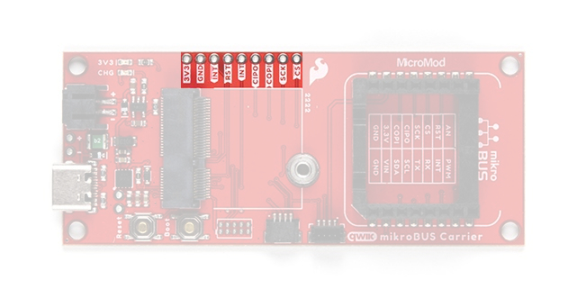
Breakout Pins
The mikroBUS™ carrier board features a 3.3V, a ground, seven I/O breakout pins. The functionality of these pins are detailed in the table above.
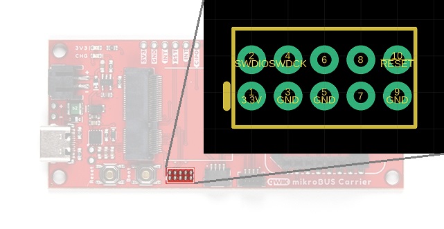
JTAG Pins
The mikroBUS™ carrier board includes JTAG PTH pins for a JTAG header, to be used with one of the recommended MikroElektronica mikroProg programmers. The JTAG pins breakout the SWD (software debug) pins to the MicroMod processor board.
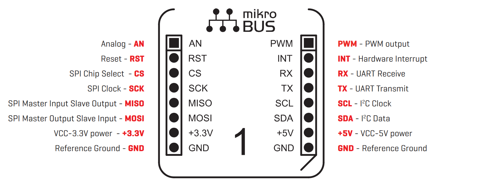
mikroBUS™ Socket
The most significant feature of this board, is the addition of the mikroBUS™ socket, which provides a drop-in interface for MikroElektronka's ecosystem of Click boards™ (over 1079 as of September 2021).
The mikroBUS™ socket comprises a pair of 8-pin female headers with a standardized pin configuration. The pins consists of three groups of communications pins (SPI, UART and I2C), six additional pins (PWM, Interrupt, Analog input, Reset and Chip select), and two power groups (3.3V and 5V).
|
mikroBUS™ Socket
Pin Name |
Carrier Board's
Processor Pin |
mikroBUS™ Socket
I/O Direction |
Description |
|---|---|---|---|
| 5V | USB_VIN | Input | Power supply: 4.75~5.5V |
| 3.3V | 3.3V | Input | Power supply: 3.3V |
| GND | - | - | Ground |
| SCK | SCK (57) | Input | SPI - Clock signal |
| CIPO | CIPO (59) | Output | SPI - Data from mikroBUS™ socket |
| COPI | COPI (61) | Input | SPI - Data to mikroBUS™ socket |
| CS | CS0 (55) | Input | SPI - Chip select for mikroBUS™ socket |
| SCL | SCL (14) | Input/Output | I2C - Clock signal |
| SDA | SDA (12) | Input/Output | I2C - Data signal to/from mikroBUS™ socket |
| TX | TX1 (17) | Input | TX - Serial data to mikroBUS™ socket |
| RX | RX1 (19) | Output | RX - Serial data from mikroBUS™ socket |
| RST | D1 (18) | Input | Reset signal to mikroBUS™ socket |
| INT | D0 (10) | Output | Interrupt trigger from mikroBUS™ socket |
| AN | A0 (34) | Output | Analog output from mikroBUS™ socket |
| PWM | PWM0 (32) | Input | PWM signal to mikroBUS™ socket |
*For more information about the mikroBUS™ socket, click here for the mikroBUS™ standard specifications.
Qwiic Connector
The Qwiic connectors are provided for users to seamlessly integrate with SparkFun's Qwiic Ecosystem.
What is Qwiic?
The Qwiic system is intended a quick, hassle-free cabling/connector system for I2C devices. Qwiic is actually a play on words between "quick" and I2C or "iic".
Features of the Qwiic System
Keep your soldering iron at bay.
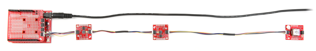
Cables plug easily between boards making quick work of setting up a new prototype. We currently offer three different lengths of Qwiic cables as well as a breadboard friendly cable to connect any Qwiic enabled board to anything else. Initially you may need to solder headers onto the shield to connect your platform to the Qwiic system but once that’s done it’s plug and go!
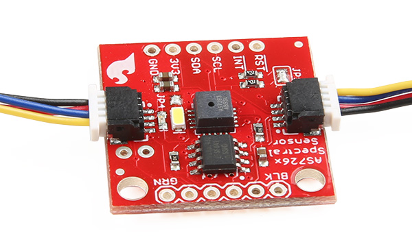
Qwiic cables connected to Spectral Sensor Breakout
Minimize your mistakes.
How many times have you swapped the SDA and SCL wires on your breadboard hoping the sensor will start working? The Qwiic connector is polarized so you know you’ll have it wired correctly, every time, from the start.
The PCB connector is part number SM04B-SRSS (Datasheet) or equivalent. The mating connector used on cables is part number SHR04V-S-B or equivalent. This is a common and low cost connector.
1mm pitch, 4-pin JST connector
Expand with ease.
It’s time to leverage the power of the I2C bus! Most Qwiic boards will have two or more connectors on them allowing multiple devices to be connected.