MicroMod Main Board Hookup Guide
 bboyho,
  Elias The Sparkiest
Hardware Overview
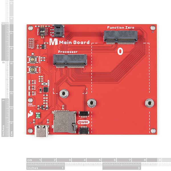
The overall functionality of the Single and Double Main Boards are the same. We'll use the Single Main Board more in this section to highlight the features since this is also included in the Double Main Board. We'll switch to the Double Main Board when necessary to highlight the features that are only included in the Double Main Board.
The only differences are that the Double Main Board includes:
- two jumper shunts
- ability to add a second MicroMod Function Board to the mix
- board's width
 |
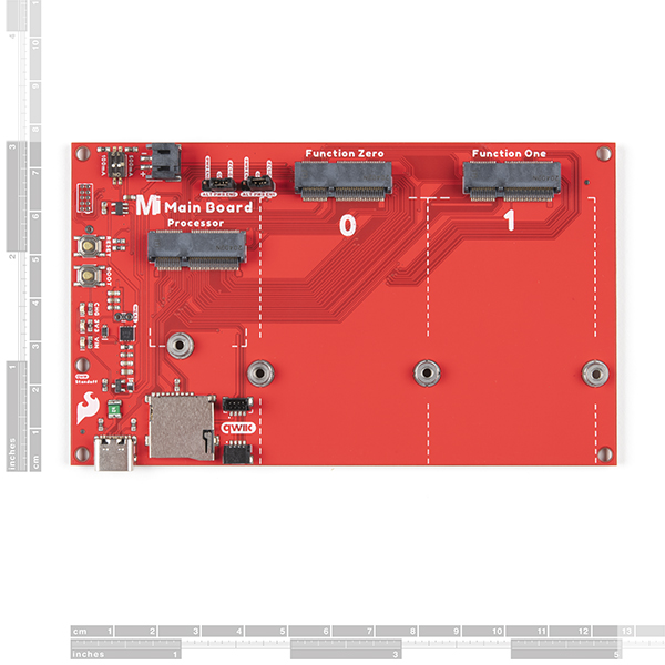 |
| Main Board - Single Measurements | Main Board - Double Measurements (Zoomed Out) |
Power
There are two ways to power the Main Boards, Processor Board, and Function Board(s).
- USB
- Single Cell LiPo Battery
It is fine to connect a power source to the USB connector and LiPo battery's JST connector at the same time. The MicroMod Main Board has power-control circuitry to automatically select the best power source.
Power USB
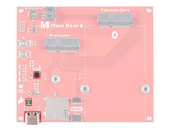
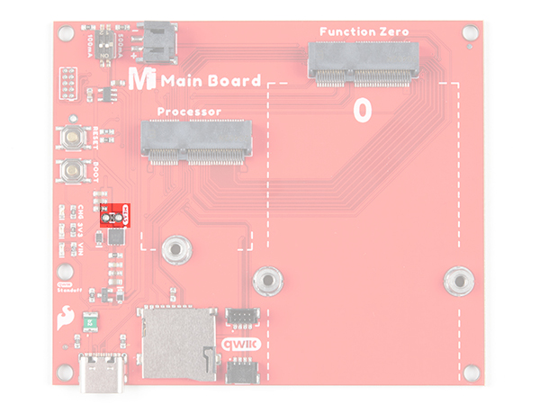
One option of powering the board is through the USB Type C connector. You will need a USB Type C cable to power the board with 5V. Power connected to the board's USB C connector will go through a resettable PTC fuse (rated at 2A max) and then the AP7361C 3.3V voltage regulator (rated at 1A max). The little green component close to the USB connector is the resettable PTC fuse while the square IC is the voltage regulator. The voltage regulator accepts voltages between ~3.3V to 6.0V.
The USB Type C connector is also used to upload code to your Processor Board, send serial data to a terminal window, or charge the LiPo battery. Of course for portable power, you could connect a USB battery as an alternative to using a LiPo battery.
Power applied to the connector will light up the VIN and 3V3 LED. If you decide to bypass the PTC fuse, simply add a solder blob to the jumper labeled as PTC. There is also a jumper labeled as MEAS to measure the current consumption at the output of the 3.3V voltage regulator for your project.
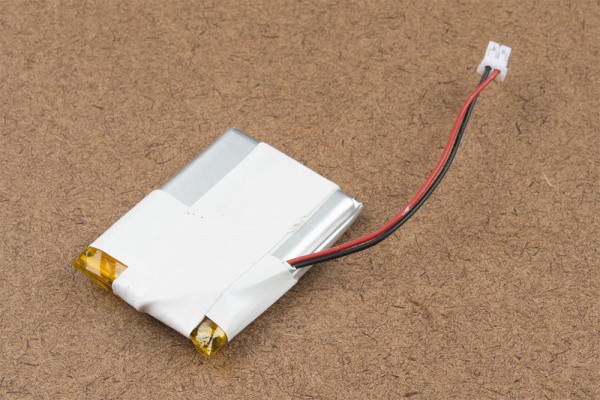
Power LiPo
The other option is to connect a single cell LiPo battery (i.e. nominal 3.7V, 4.2V fully charged) to the 2-pin JST connector as shown below. A MCP73831 charge IC is included on the boards to safely charge the LiPo batteries via USB Type C connector. A switch is included to set the charge rate. The charge rate is probably set to ~166mA with both switches flipped to the ON position. This may vary depending on the position of the switch when it was pulled from the reel. Flip the switch to adjust the charge rate to either 100mA or 500mA using a precision flat head screw driver or tweezers.
The voltage from the LiPo battery is regulated down to 3.3V as it goes through the AP7361C 3.3V voltage regulator (rated at 1A max).
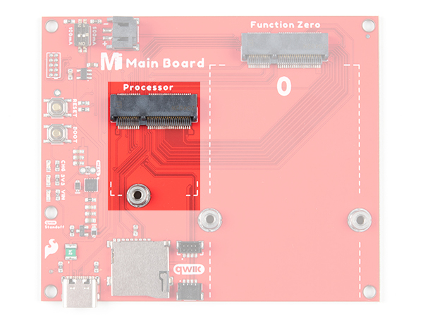
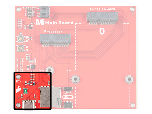
MicroMod Processor Board
The MicroMod ecosystem allows you to easily swap out processors depending on your application. The location of the M.2 connector labeled as Processor is where you would connect and secure a MicroMod Processor Board.
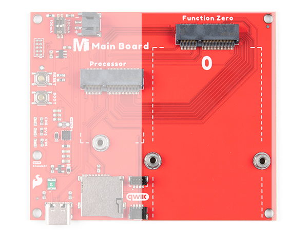
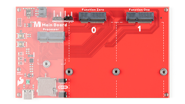
MicroMod Function Board
Beside the MicroMod Processor's socket is another M.2 connector for MicroMod Function Boards, which allow you to add additional functionality to your Processor Board. The Single Main Board includes one socket for a single Function Board while the Double Main Board includes two sockets for up two Function Boards.
 |
 |
| Main Board - Single Function Board Socket | Main Board - Double Function Board Sockets |
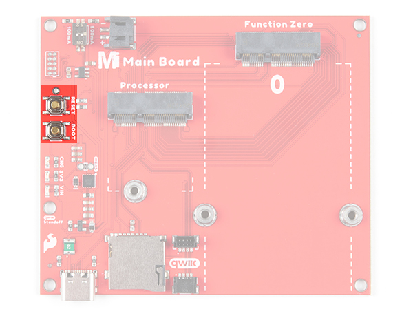
Reset and Boot Buttons
Each board includes a reset and boot button. There is an additional reset button PTH next to the reset button. Hitting the reset button to restart your Processor Board. Hitting the boot button will put the Processor Board into a special boot mode. Depending on the processor board, this boot pin may not be connected.
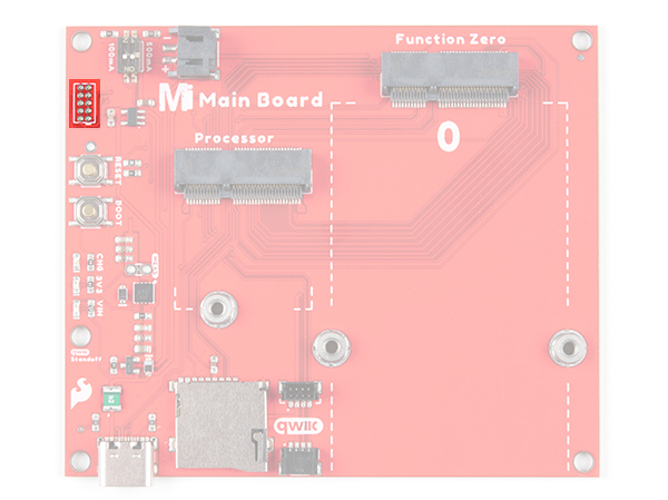
SWD Pins
For advanced users, we broke out the 2x5 SWD programming pins. Note that this is not populated so you will need a compatible header and compatible JTAG programmer to connect.
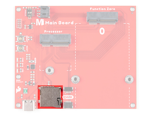
MicroSD Socket
The board includes a microSD socket if your application requires you to log and save data to a memory card. The primary SPI pins (SDO, SDI, SCK, CS0) from your Processor and Function Board are connected to the microSD Socket.
D1 while the MicroMod Main Board - Double is on the Processor Board's G4.
LEDs
There are three LEDs on the board:
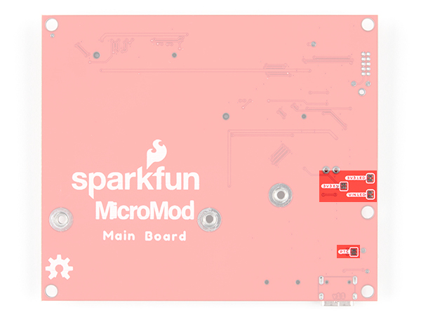
- VIN - The VIN LED lights up to indicate when power available from the USB connector.
- 3V3 - The 3V3 LED lights up to indicate when there is a 3.3V available after power is regulated down from the USB connector or LiPo battery.
- CHG - The on-board yellow CHG LED can be used to get an indication of the charge status of your battery. Below is a table of other status indicators depending on the state of the charge IC.
| Charge State | LED status |
| No Battery | Floating (should be OFF, but may flicker) |
| Shutdown | Floating (should be OFF, but may flicker) |
| Charging | ON |
| Charge Complete | OFF |
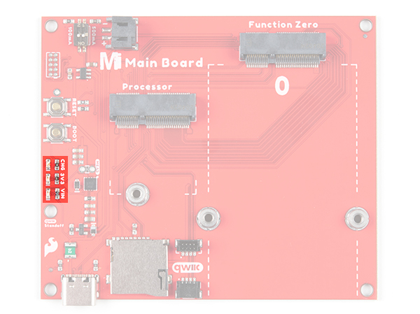
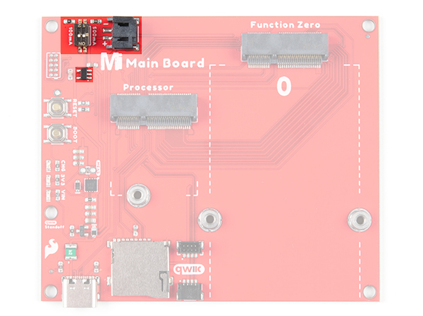
Jumpers
The following five jumpers are included on both the Single and Double Main Boards.
- MEAS - By default, the jumper is closed and located on the top side of the board. This jumper is used to measure your system's current consumption. You can cut this jumper's trace and connect the PTHs to a ammeter/multimeter to probe the output from the 3.3V voltage regulator. Check out our How to Use a Multimeter tutorial for more information on measuring current.
- PTC - By default, the jumper is open and located on the bottom of the board. For advanced users that know what you are doing, add a solder blob to the jumper to bypass the resettable PTC fuse to pull more than 2A from the USB source.
- 3.3V EN - By default, this jumper is open and located on the bottom of the board. Closing this jumper enables processor control of the 3.3V bus.
- VIN LED - By default, this jumper is closed and located on the bottom of the board. Cut this trace to disable the LED that is connected to the input of the USB
- 3.3V LED - By default, this jumper is closed and located on the bottom of the board. Cut this trace to disable the LED that is connected to the output of the 3.3V voltage regulator.
 |
 |
| Main Board - Single Top View Jumpers |
Main Board - Single Bottom View Jumpers |
Included only on the Double Main Board are two 1x3 male headers with 2-pin jumper shunts to enable the 3.3V voltage regulator for any Function Board connected to Function Zero and Function One using alternative Processor GPIO pins. Since certain processors have limited GPIO and may not be broken out on certain locations, alternative pins have been provided on the board. The ALT PWR EN0 jumper allows users to control the 3.3V voltage regulator on any Function Board that is connected to Function Zero. When the jumper shunt is on the left side toward the 2-pin JST connector, the jumper shunt connects the PWR EN0 to the Processor Board's GPIO G5 pin. Moving the jumper shunt to the other side connects the Processor Board's GPIO G5 pin to Function Board One's GPIO G3 pin.
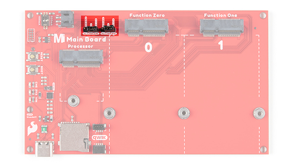
The ALT PWR EN1 jumper allows users control power from the 3.3V voltage regulator for any Function Board that is connected to Function One when the jumper shunt is connecting PWR EN1 and Processor Board's GPIO G6 pin. Moving the jumper shunt to the other side connects the Processor Board's GPIO G6 pin to Function Board One's GPIO G4 pin.
Qwiic and I2C
The board includes a vertical and horizontal Qwiic connector. These are connected to the primary I2C bus and 3.3V power on both the Processor and Function Board connectors allowing you to easily add a Qwiic-enabled device to your application.
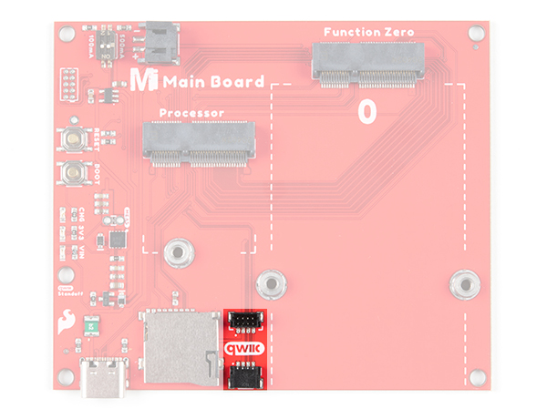
Note that there are two mounting holes for Qwiic-enabled boards that have a standard 1.0"x1.0" size board. The image below highlighted with a black square is where you would place the board.
MicroMod Pinout
Depending on your window size, you may need to use the horizontal scroll bar at the bottom of the table to view the additional pin functions. Note that the M.2 connector pins on opposing sides are offset from each other as indicated by the bottom pins where it says (Not Connected)*. There is no connection to pins that have a "-" under the primary function.
| AUDIO | UART | GPIO/BUS | I2C | SDIO | SPI | Dedicated |
| Processor Pins | Function Zero Pins | Main Board - Single Miscellaneous Pins |
|---|---|---|
| GND | GND | GND |
| 3.3V | - | 3.3V |
| USB_D+_Processor | - | USB_D+ |
| 3.3V_EN | - | 3.3V_EN |
| USB_D-_Processor | - | USB_D- |
| RESET# (I - Open Drain) | - | RESET# (I - Open Drain) |
| GND | GND | GND |
| USB_VIN | - | USB_VIN |
| D0_Processor | F0 | - |
| BOOT (I - Open Drain) | - | BOOT (I - Open Drain) |
| I2C_SDA_Processor | I2C_SDA | I2C_SDA (Qwiic) |
| UART_RTS_Processor | UART_RTS | - |
| I2C_SCL_Processor | I2C_SCL | I2C_SCL (Qwiic) |
| UART_CTS_Processor | UART_CTS | - |
| I2C_INT_Processor | I2C_INT | - |
| UART_TX_Processor | UART_RX | - |
| D1_Processor | - | SD Card CS (microSD Card) |
| UART_RX_Processor | UART_TX | - |
| SWDCK_Processor | - | SWDCK (2x5 Header) |
| SWDIO_Processor | - | SWDCK (2x5 Header) |
| PWM0_Processor | PWM0 | - |
| GND | GND | GND |
| A0_Processor | A0 | - |
| USBHOST_D+_Processor | USBHOST_D+ | - |
| GND | GND | GND |
| USBHOST_D-_Processor | USBHOST_D- | - |
| A1_Processor | PWR_EN0 | - |
| GND | GND | GND |
| G0_Processor | F3 | - |
| CAN_RX_Processor | CAN_TX | - |
| G1_Processor | F4 | - |
| CAN_TX_Processor | CAN_RX | - |
| G2_Processor | F5 | - |
| GND | GND | GND |
| G3_Processor | F6 | - |
| G4_Processor | F7 | - |
| BATT_VIN / 3 (I - ADC) (0 to 3.3V) | - | BATT_VIN / 3 (I - ADC) (0 to 3.3V) |
| SPI_CS0_Processor | F1 | - |
| SPI_SCK_Processor | SPI_SCK | SPI_SCK (microSD Card) |
| SPI_DI_Processor | SPI_DO | SPI_DO (microSD Card) |
| SPI_DO_Processor | SPI_DI | SPI_DI (microSD Card) |
| SDIO_DATA2_Processor | PWR_EN0 | - |
| Processor Pins | Function Zero Pins | Function One Pins | Main Board - Double Miscellaneous Pins |
|---|---|---|---|
| GND | GND | GND | GND |
| 3.3V | - | - | 3.3V |
| USB_D+_Processor | - | - | USB_D+ |
| 3.3V_EN | - | - | 3.3V_EN |
| USB_D-_Processor | - | - | USB_D- |
| RESET# (I - Open Drain) | - | - | RESET# (I - Open Drain) |
| GND | GND | GND | GND |
| - | - | - | - |
| USB_VIN | - | - | USB_VIN |
| D0_Processor | F0 | - | - |
| BOOT (I - Open Drain) | - | - | BOOT (I - Open Drain) |
| I2C_SDA_Processor | I2C_SDA | I2C_SDA | I2C_SDA (Qwiic) |
| UART1_RTS_Processor | UART_RTS | (No Flow Control) | - |
| I2C_SCL_Processor | I2C_SCL | I2C_SCL | I2C_SCL (Qwiic) |
| UART_CTS_Processor | UART_CTS | (No Flow Control) | - |
| I2C_INT_Processor | I2C_INT | I2C_INT | - |
| UART1_TX_Processor | UART_RX | - | - |
| D1_Processor | - | F0 | - |
| UART1_RX_Processor | UART_TX | - | - |
| UART2_RX_Processor | - | UART_TX | - |
| SWDCK_Processor | - | - | SWDCK (2x5 Header) |
| UART2_TX_Processor | - | UART_RX | - |
| SWDIO_Processor | - | - | SWDCK (2x5 Header) |
| PWM0_Processor | PWM | - | - |
| GND | GND | GND | GND |
| A0_Processor | A0 | - | - |
| USBHOST_D+_Processor | USBHOST_D+ | (No USB Host) | - |
| GND | GND | GND | GND |
| USBHOST_D-_Processor | USBHOST_D- | (No USB Host) | - |
| A1_Processor | - | A0 | - |
| GND | GND | GND | GND |
| G0_Processor | F3 | - | - |
| CAN_RX_Processor | CAN_TX | (No CAN BUS) | - |
| G1_Processor | F4 | - | - |
| CAN_TX_Processor | CAN_RX | (No CAN BUS) | - |
| G2_Processor | F5 | - | - |
| GND | GND | GND | GND |
| G3_Processor | F6 | - | - |
| PWM1_Processor | - | PWM | - |
| G4_Processor | F7 | - | SD Card CS (microSD Card) |
| BATT_VIN / 3 (I - ADC) (0 to 3.3V) | - | - | BATT_VIN / 3 (I - ADC) (0 to 3.3V) |
| - | - | - | - |
| - | - | - | - |
| - | - | - | - |
| - | - | - | - |
| - | - | - | - |
| SPI_CS0_Processor | F1 | - | - |
| - | - | - | - |
| SPI_SCK_Processor | SPI_SCK | SPI_SCK | SPI_SCK (microSD Card) |
| - | - | - | - |
| SPI_DI_Processor | SPI_DO | SPI_DO | SPI_DO (microSD Card) |
| SDIO_CLK_Processor | - | F7 | - |
| SPI_DO_Processor | SPI_DI | SPI_DI | SPI_DI (microSD Card) |
| SDIO_CMD_Processor | - | F6 | - |
| - | - | - | - |
| - | - | - | - |
| - | - | - | - |
| SDIO_DATA1_Processor | - | PWR_EN1 | - |
| - | - | - | - |
| SDIO_DATA2_Processor | PWR_EN0 | - | - |
| G7_Processor | - | F5 | - |
| SPI_CS1_Processor | - | SPI_CS1 | - |
| G6_Processor | - | F4 | - |
| - | - | - | - |
| Alternative Function |
Primary Function |
Bottom Pin |
Top Pin |
Primary Function |
Alternative Function |
|---|---|---|---|---|---|
| (Not Connected) | 75 | GND | |||
| VIN | 74 | 73 | 3.3V | ||
| VIN | 72 | 71 | Power EN | ||
| - | 70 | 69 | - | ||
| - | 66 | 65 | - | ||
| - | 64 | 63 | - | ||
| - | 62 | 61 | F7 | ||
| - | 60 | 59 | F6 | ||
| - | 58 | 57 | F5 | ||
| - | 56 | 55 | F4 | ||
| - | 54 | 53 | F3 | ||
| - | 52 | 51 | F2 | PWM | |
| - | 50 | 49 | F1 | SPI_CS0 | |
| - | 48 | 47 | F0 | INT | |
| - | 46 | 45 | GND | ||
| - | 44 | 43 | CAN_TX | ||
| - | 42 | 41 | CAN_RX | ||
| - | 40 | 39 | GND | ||
| A0 | 38 | 37 | USBHOST_D- | ||
| EEPROM_A0 | 36 | 35 | USBHOST_D+ | ||
| EEPROM_A1 | 34 | 33 | GND | ||
| EEPROM_A2 | 32 | 31 | Module Key | ||
| Module Key | 30 | 29 | Module Key | ||
| Module Key | 28 | 27 | Module Key | ||
| Module Key | 26 | 25 | Module Key | ||
| Module Key | 24 | 23 | I2C_INT | ||
| - | 22 | 21 | I2C_SCL | ||
| - | 20 | 19 | I2C_SDA | ||
| UART_CTS | 18 | 17 | - | ||
| UART_RTS | 16 | 15 | UART_RX | ||
| - | 14 | 13 | UART_TX | ||
| - | 12 | 11 | - | ||
| - | 10 | 9 | - | ||
| - | 8 | 7 | SPI_SDO | ||
| - | 6 | 5 | SPI_SDI | ||
| - | 4 | 3 | SPI_SCK | ||
| - | 2 | 1 | GND |
| Alternative Function | Alternative Function | Alternative Function | Primary Function | Bottom Pin |
Top Pin |
Primary Function | Alternative Function | Alternative Function | Alternative Function |
|---|---|---|---|---|---|---|---|---|---|
| (Not Connected) | 75 | GND | |||||||
| 3.3V | 74 | 73 | G5 / BUS5 | ||||||
| RTC_3V_BATT | 72 | 71 | G6 / BUS6 | ||||||
| SPI_CS1# | SDIO_DATA3 (I/O) | 70 | 69 | G7 / BUS7 | |||||
| SDIO_DATA2 (I/O) | 68 | 67 | G8 | ||||||
| SDIO_DATA1 (I/O) | 66 | 65 | G9 | ADC_D- | CAM_HSYNC | ||||
| SPI_CIPO1 | SDIO_DATA0 (I/O) | 64 | 63 | G10 | ADC_D+ | CAM_VSYNC | |||
| SPI COPI1 | SDIO_CMD (I/O) | 62 | 61 | SPI_CIPO (I) | |||||
| SPI SCK1 | SDIO_SCK (O) | 60 | 59 | SPI_COPI (O) | LED_DAT | ||||
| AUD_MCLK (O) | 58 | 57 | SPI_SCK (O) | LED_CLK | |||||
| CAM_MCLK | PCM_OUT | I2S_OUT | AUD_OUT | 56 | 55 | SPI_CS# | |||
| CAM_PCLK | PCM_IN | I2S_IN | AUD_IN | 54 | 53 | I2C_SCL1 (I/O) | |||
| PDM_DATA | PCM_SYNC | I2S_WS | AUD_LRCLK | 52 | 51 | I2C_SDA1 (I/O) | |||
| PDM_CLK | PCM_CLK | I2S_SCK | AUD_BCLK | 50 | 49 | BATT_VIN / 3 (I - ADC) (0 to 3.3V) | |||
| G4 / BUS4 | 48 | 47 | PWM1 | ||||||
| G3 / BUS3 | 46 | 45 | GND | ||||||
| G2 / BUS2 | 44 | 43 | CAN_TX | ||||||
| G1 / BUS1 | 42 | 41 | CAN_RX | ||||||
| G0 / BUS0 | 40 | 39 | GND | ||||||
| A1 | 38 | 37 | USBHOST_D- | ||||||
| GND | 36 | 35 | USBHOST_D+ | ||||||
| A0 | 34 | 33 | GND | ||||||
| PWM0 | 32 | 31 | Module Key | ||||||
| Module Key | 30 | 29 | Module Key | ||||||
| Module Key | 28 | 27 | Module Key | ||||||
| Module Key | 26 | 25 | Module Key | ||||||
| Module Key | 24 | 23 | SWDIO | ||||||
| UART_TX2 (O) | 22 | 21 | SWDCK | ||||||
| UART_RX2 (I) | 20 | 19 | UART_RX1 (I) | ||||||
| CAM_TRIG | D1 | 18 | 17 | UART_TX1 (0) | |||||
| I2C_INT# | 16 | 15 | UART_CTS1 (I) | ||||||
| I2C_SCL (I/0) | 14 | 13 | UART_RTS1 (O) | ||||||
| I2C_SDA (I/0) | 12 | 11 | BOOT (I - Open Drain) | ||||||
| D0 | 10 | 9 | USB_VIN | ||||||
| SWO | G11 | 8 | 7 | GND | |||||
| RESET# (I - Open Drain) | 6 | 5 | USB_D- | ||||||
| 3.3V_EN | 4 | 3 | USB_D+ | ||||||
| 3.3V | 2 | 1 | GND |
| Signal Group | Signal | I/O | Description | Voltage | Power | 3.3V | I | 3.3V Source | 3.3V |
|---|---|---|---|---|
| GND | Return current path | 0V | ||
| USB_VIN | I | USB VIN compliant to USB 2.0 specification. Connect to pins on processor board that require 5V for USB functionality | 4.8-5.2V | |
| RTC_3V_BATT | I | 3V provided by external coin cell or mini battery. Max draw=100μA. Connect to pins maintaining an RTC during power loss. Can be left NC. | 3V | |
| 3.3V_EN | O | Controls the carrier board's main voltage regulator. Voltage above 1V will enable 3.3V power path. | 3.3V | |
| BATT_VIN/3 | I | Carrier board raw voltage over 3. 1/3 resistor divider is implemented on carrier board. Amplify the analog signal as needed for full 0-3.3V range | 3.3V | |
| Reset | Reset | I | Input to processor. Open drain with pullup on processor board. Pulling low resets processor. | 3.3V |
| Boot | I | Input to processor. Open drain with pullup on processor board. Pulling low puts processor into special boot mode. Can be left NC. | 3.3V | |
| USB | USB_D± | I/O | USB Data ±. Differential serial data interface compliant to USB 2.0 specification. If UART is required for programming, USB± must be routed to a USB-to-serial conversion IC on the processor board. | |
| USB Host | USBHOST_D± | I/O | For processors that support USB Host Mode. USB Data±. Differential serial data interface compliant to USB 2.0 specification. Can be left NC. | |
| CAN | CAN_RX | I | CAN Bus receive data. | 3.3V |
| CAN_TX | O | CAN Bus transmit data. | 3.3V | |
| UART | UART_RX1 | I | UART receive data. | 3.3V |
| UART_TX1 | O | UART transmit data. | 3.3V | |
| UART_RTS1 | O | UART ready to send. | 3.3V | |
| UART_CTS1 | I | UART clear to send. | 3.3V | |
| UART_RX2 | I | 2nd UART receive data. | 3.3V | |
| UART_TX2 | O | 2nd UART transmit data. | 3.3V | |
| I2C | I2C_SCL | I/O | I2C clock. Open drain with pullup on carrier board. | 3.3V |
| I2C_SDA | I/O | I2C data. Open drain with pullup on carrier board | 3.3V | |
| I2C_INT# | I | Interrupt notification from carrier board to processor. Open drain with pullup on carrier board. Active LOW | 3.3V | |
| I2C_SCL1 | I/O | 2nd I2C clock. Open drain with pullup on carrier board. | 3.3V | |
| I2C_SDA1 | I/O | 2nd I2C data. Open drain with pullup on carrier board. | 3.3V | |
| SPI | SPI_COPI | O | SPI Controller Output/Peripheral Input. | 3.3V |
| SPI_CIPO | I | SPI Controller Input/Peripheral Output. | 3.3V | |
| SPI_SCK | O | SPI Clock. | 3.3V | |
| SPI_CS# | O | SPI Chip Select. Active LOW. Can be routed to GPIO if hardware CS is unused. | 3.3V | |
| SPI/SDIO | SPI_SCK1/SDIO_CLK | O | 2nd SPI Clock. Secondary use is SDIO Clock. | 3.3V |
| SPI_COPI1/SDIO_CMD | I/O | 2nd SPI Controller Output/Peripheral Input. Secondary use is SDIO command interface. | 3.3V | |
| SPI_CIPO1/SDIO_DATA0 | I/O | 2nd SPI Peripheral Input/Controller Output. Secondary use is SDIO data exchange bit 0. | 3.3V | |
| SDIO_DATA1 | I/O | SDIO data exchange bit 1. | 3.3V | |
| SDIO_DATA2 | I/O | SDIO data exchange bit 2. | 3.3V | |
| SPI_CS1/SDIO_DATA3 | I/O | 2nd SPI Chip Select. Secondary use is SDIO data exchange bit 3. | 3.3V | |
| Audio | AUD_MCLK | O | Audio master clock. | 3.3V |
| AUD_OUT/PCM_OUT/I2S_OUT/CAM_MCLK | O | Audio data output. PCM synchronous data output. I2S serial data out. Camera master clock. | 3.3V | |
| AUD_IN/PCM_IN/I2S_IN/CAM_PCLK | I | Audio data input. PCM syncrhonous data input. I2S serial data in. Camera periphperal clock. | 3.3V | |
| AUD_LRCLK/PCM_SYNC/I2S_WS/PDM_DATA | I/O | Audio left/right clock. PCM syncrhonous data SYNC. I2S word select. PDM data. | 3.3V | |
| AUD_BCLK/PCM_CLK/I2S_CLK/PDM_CLK | O | Audio bit clock. PCM clock. I2S continuous serial clock. PDM clock. | 3.3V | |
| SWD | SWDIO | I/O | Serial Wire Debug I/O. Connect if processor board supports SWD. Can be left NC. | 3.3V |
| SWDCK | I | Serial Wire Debug clock. Connect if processor board supports SWD. Can be left NC. | 3.3V | |
| ADC | A0 | I | Analog to digital converter 0. Amplify the analog signal as needed to enable full 0-3.3V range. | 3.3V |
| A1 | I | Analog to digital converter 1. Amplify the analog signal as needed to enable full 0-3.3V range. | 3.3V | |
| PWM | PWM0 | O | Pulse width modulated output 0. | 3.3V |
| PWM1 | O | Pulse width modulated output 1. | 3.3V | |
| Digital | D0 | I/O | General digital input/output pin. | 3.3V |
| D1/CAM_TRIG | I/O | General digital input/output pin. Camera trigger. | 3.3V | |
| General/Bus | G0/BUS0 | I/O | General purpose pins. Any unused processor pins should be assigned to Gx with ADC + PWM capable pins given priority (0, 1, 2, etc.) positions. The intent is to guarantee PWM, ADC and Digital Pin functionality on respective ADC/PWM/Digital pins. Gx pins do not guarantee ADC/PWM function. Alternative use is pins can support a fast read/write 8-bit or 4-bit wide bus. | 3.3V |
| G1/BUS1 | I/O | 3.3V | ||
| G2/BUS2 | I/O | 3.3V | ||
| G3/BUS3 | I/O | 3.3V | ||
| G4/BUS4 | I/O | 3.3V | ||
| G5/BUS5 | I/O | 3.3V | ||
| G6/BUS6 | I/O | 3.3V | ||
| G7/BUS7 | I/O | 3.3V | ||
| G8 | I/O | General purpose pin | 3.3V | |
| G9/ADC_D-/CAM_HSYNC | I/O | Differential ADC input if available. Camera horizontal sync. | 3.3V | |
| G10/ADC_D+/CAM_VSYNC | I/O | Differential ADC input if available. Camera vertical sync. | 3.3V | |
| G11/SWO | I/O | General purpose pin. Serial Wire Output | 3.3V |
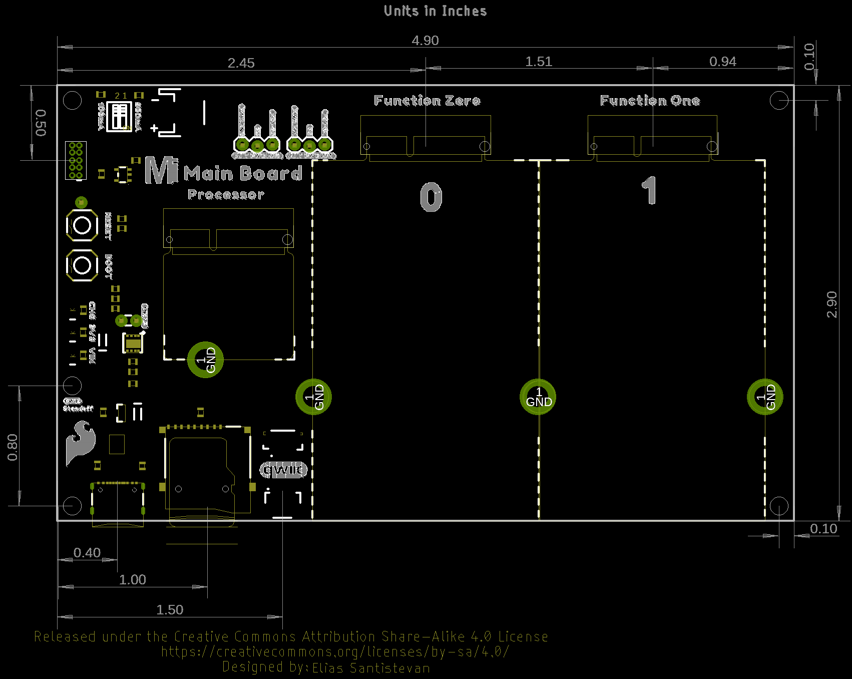
Board Dimensions
The board dimension of the MicroMod Main Board - Single is 2.90" x 3.40" while the MicroMod Main Board - Double is 2.90" x 4.90". Both boards include 5x mounting holes. Four are located on the edge of each board. The fifth mounting hole is located 0.80" away from another mounting hole to mount Qwiic-enabled boards that have the standard 1.0"x1.0" size board.
 |
 |
| MicroMod Main Board - Single | MicroMod Main Board - Double |