MicroMod GNSS Function Board - ZED-F9P Hookup Guide
 El Duderino
Hardware Overview
Let's take a closer look at the ZED-F9P module and other hardware on this Function Board.
ZED-F9P GNSS Module
The ZED-F9P is a high-precision GNSS module from u-blox capable of up to millimeter X, Y & Z positional accuracy.
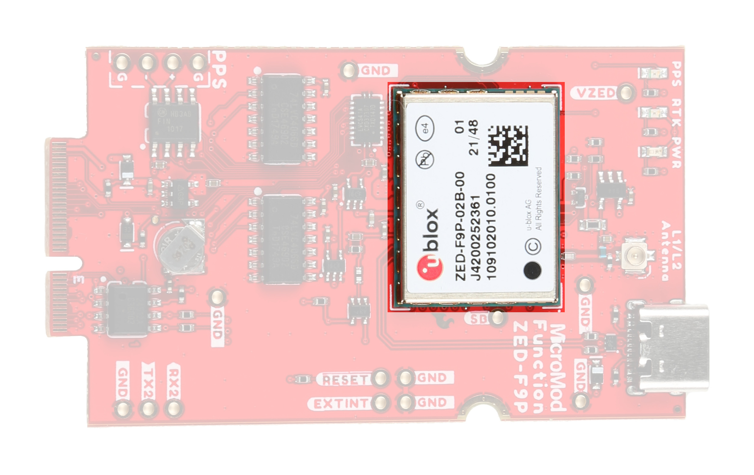
The ZED-F9P with a full RTK lock along with RTCM data streaming to the module can achieve 10mm 3D positional accuracy. Depending on the constellation the module achieves a lock in ~25 seconds from a cold start and 2 seconds from both a hot start and aided start. For a complete overview of the module, refer to the ZED-F9P datasheet.
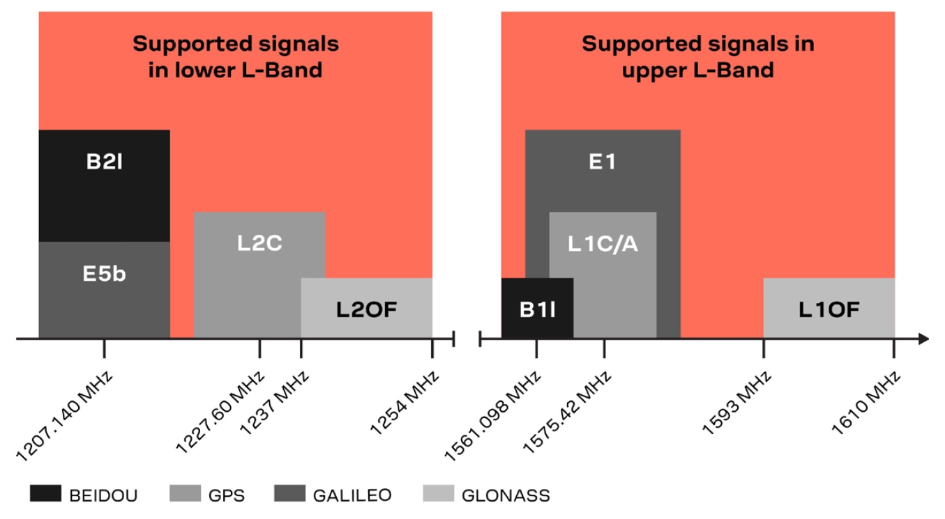
One of the key differentiators between the ZED-F9P and almost all other low-cost RTK solutions is the ZED-F9P is capable of receiving both L1 and L2 bands.
The module can act as either a rover to receive GNNS location data and RTCM correction data or a base station to send RTCM correction data to another device. For complete information on how to configure the ZED-F9P as a base station or rover, refer to the u-blox Integration Manual or check out this tutorial.
Communication Interfaces
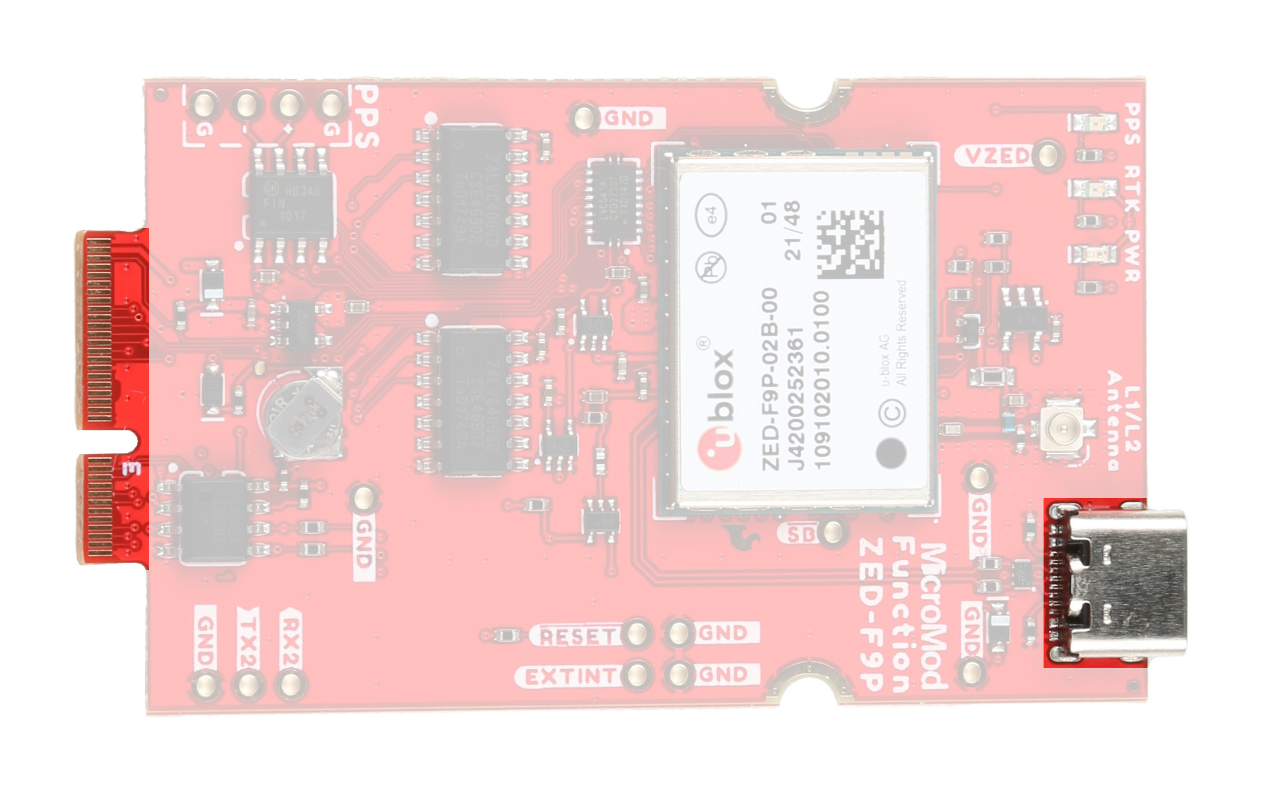
This Function Board routes the ZED-F9P's USB interface to a USB-C connector on the top of the board. The SPI, I2C and primary serial interfaces are routed to the MicroMod M.2 connector through an isolation circuit.
The board configures the ZED-F9P to communicate via I2C and Serial by default. Adjusting the DSEL solder jumper switches the communication interface to SPI.
The USB-C connector allows direct communication to the ZED-F9P UART interface but does not provide power to the module or other parts of the MicroMod assembly by default. To use this connector for power, adjust the USB PWR EN jumper. Read on to the Solder Jumpers section for more information.
Antenna
The board routes the ZED-F9P antenna connection to a u.Fl connector for an external antenna connection. Most of the recommended antennas use a SMA-type connector so an adapter like this is most likely needed.
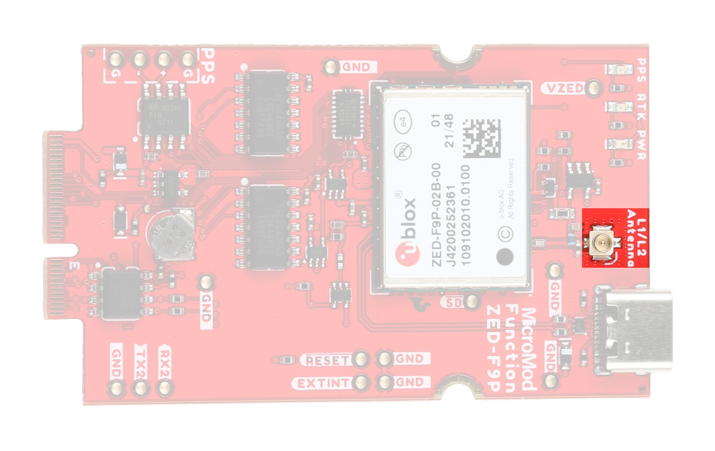
The Function Board also includes a RF/antenna supervision circuit to monitor and control the active antenna connection. The supervision circuit protects the ZED-F9P from a short circuit on the antenna connection and monitors the antenna connection to detect a connected antenna or open circuit. By default the Function Board disables this circuit through the SUP solder jumper. Read on to the Solder Jumpers section for more information on using this jumper and refer to section 4.3.4 of the ZED-F9P Integration Manual for more information on this circuit and how to poll the status using UBX messages.
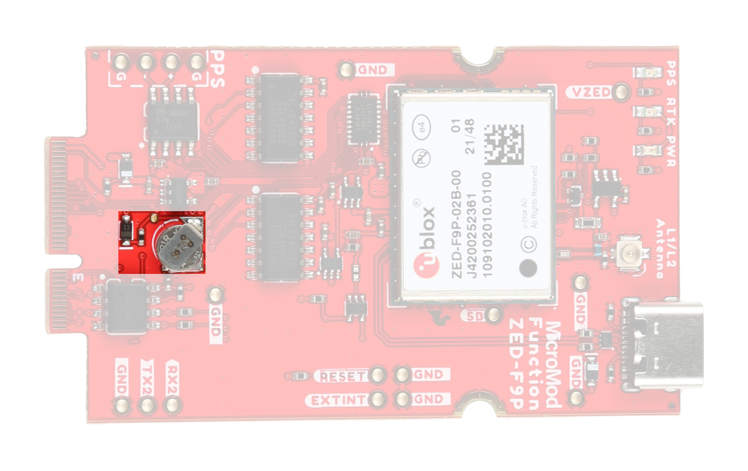
Backup Battery
The backup battery on the board has a 1.5mAh capacity to maintain settings and other low-power functionality to the ZED-F9P when the module is not fully powered.
PTH Connections
Along with the secondary serial bus, the Function Board routes several other ZED-F9P pins to plated through-hole (PTH) connecitons.
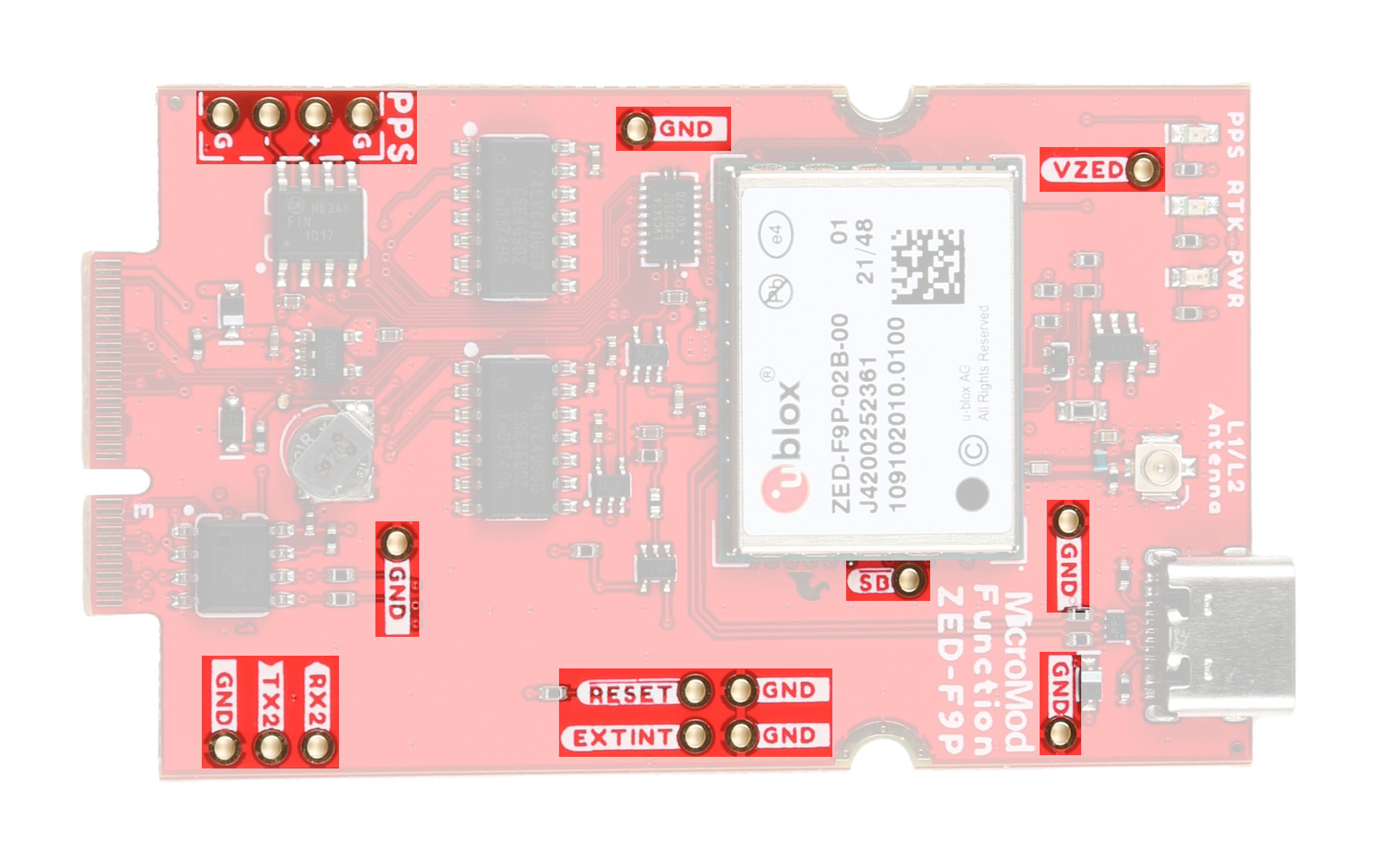
The list below outlines the labels and functionality of the PTH connections on the Function Board:
- PPS - The board translates the Pulse-Per-Second (PPS) output to a differential output routed to a pair of PTHs along with matching ground PTHs.
- RX2/TX2 - The ZED-F9P's secondary UART (RX2/TX2) along with a ground PTH.
- Reset - ZED-F9P reset pin.
- EXTINT - ZED-F9P external interrupt pin.
- SB - ZED-F9P SafeBoot pin.
- GND - Several Ground PTHs if needed.
LEDs
The GNSS Function Board - ZED-F9P has three LEDs labeled: PWR, PPS and RTK.
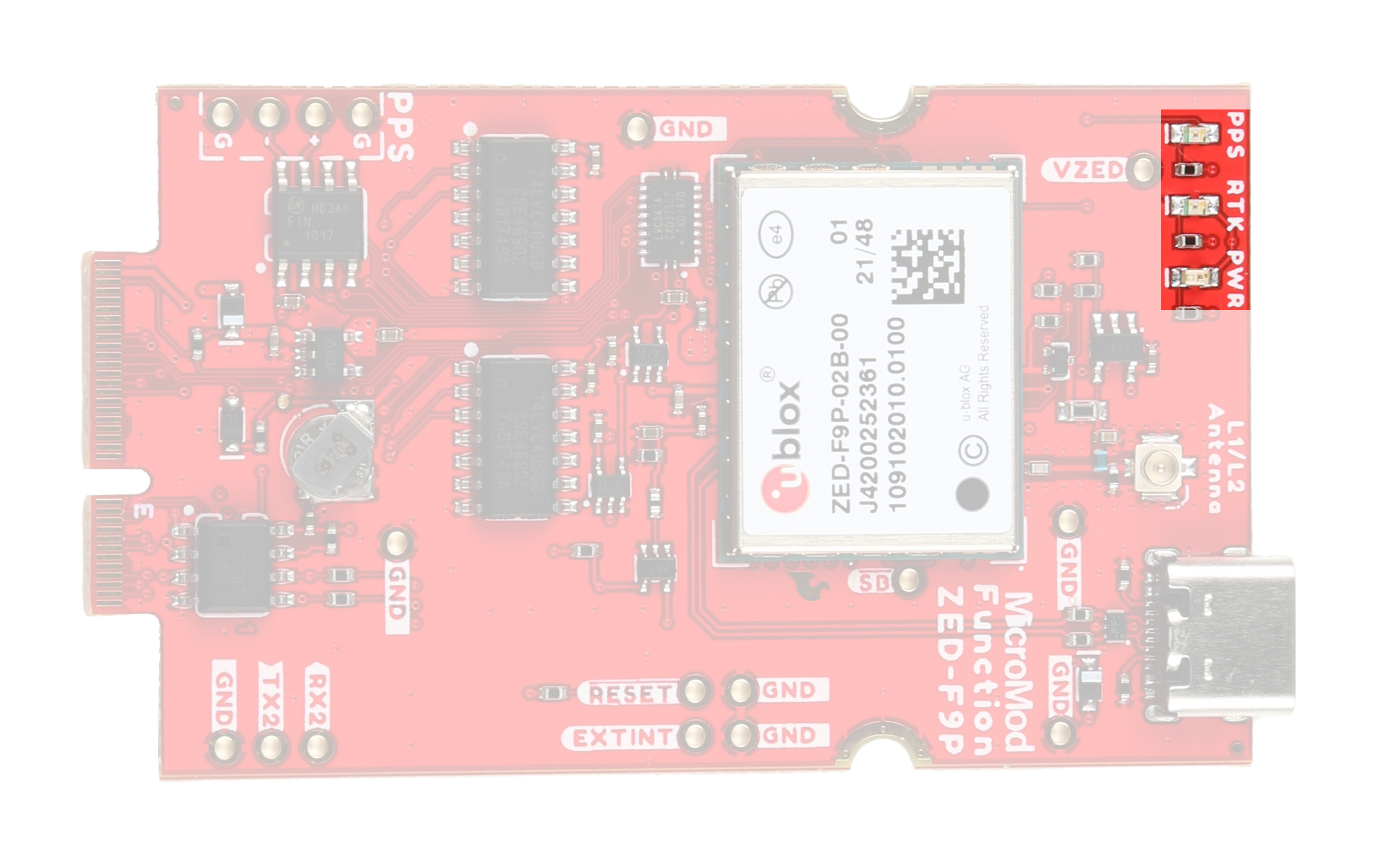
- PWR - Indicates when the ZED-F9P is powered.
- PPS - Tied to the Pulse Per Second pin and acts as a visual indicator to the ZED-F9P pulse per second signal.
- RTK - Indicates the status of the RTK lock.
Solder Jumpers
This board has nine solder jumpers. The table below outlines each jumper's label, default state, function and notes regarding their use:
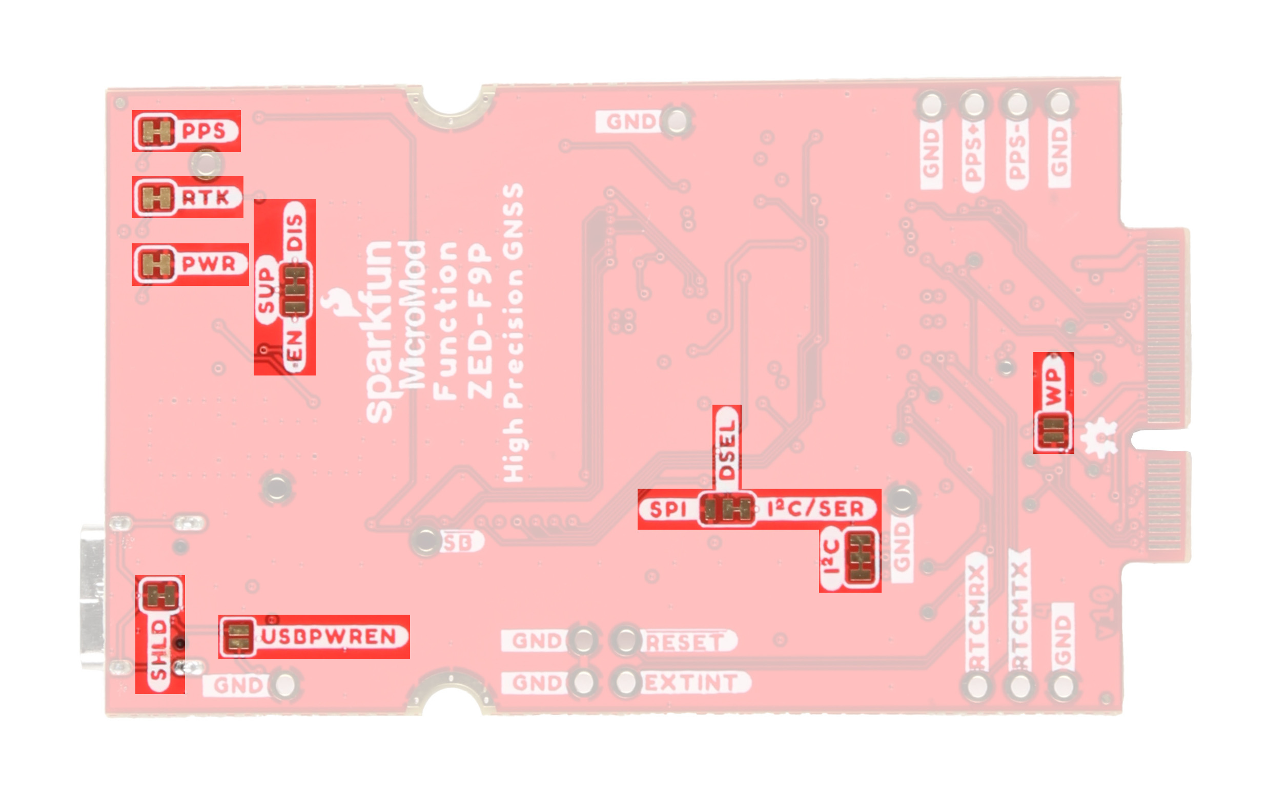
| Label | Default State | Function | Notes |
|---|---|---|---|
| USBPWREN | OPEN | Enables USB power to ZED-F9P. | Close to use the USB-C connector on the Function Board to power the ZED-F9P. |
| SHLD | CLOSED | USB-C shield control. | Open to disconnect the USB-C shield pin to the ground plane. |
| SUP | Disable | Antenna supervisor circuit control. | Disables the antenna supervisor circuit by default. Switch to EN side to enable the circuit. |
| DSEL | ZED-F9P interface selection. | I2C/Serial | Three pad jumper controls which communication interface the ZED-F9P uses. Can be set to I2C/Serial (Default) or SPI. |
| I2C | CLOSED | I2C pull up resistors | Three-way jumper pulling the SDA and SCL lines to 3.3V through a pair of 2.2kΩ resistors. Sever both traces to disable the pull up resistors. |
| WP | EEPROM Write Protection | OPEN | Close to clarification needed write protection on the EEPROM IC. |
| PWR | Power LED control. | CLOSED | Enables the ZED-F9P power indicator LED. Open to disable the LED. |
| PPS | PPS LED control. | CLOSED | Enables the ZED-F9P pulse per second LED. Open to disable the LED. |
| RTK | RTK LED control. | CLOSED | Enables the ZED-F9P RTK lock indicator LED. Open to disable the LED. |
MicroMod Pinout
This Function Board uses the following pins on a connected Processor Board:
- 3.3V & VCC
- Power enable
- SPI - ZED-F9P SPI
- I2C - ZED-F9P I2C and EEPROM
- UART RX1/TX1 (Slot 0) / UART RX2/TX2 (Slot 1) - ZED-F9P UART1
- CS0 (Slot 0) / CS1 (Slot 1) - ZED-F9P Chip Select
- D0 (Slot 0) / D1 (Slot 1) - ZED-F9P TX Ready
- PWM0 (Slot 0) / PWM1 (Slot 1) - ZED-F9P Pulse-Per-Second
- G0 (Slot 0) / G5 (Slot 1) - ZED-F9P Reset
- G1 (Slot 0) / G6 (Slot 1) - External Interrupt
- G2 (Slot 0) / G7 (Slot 1) - RTK Status
- G3 (Slot 0) / G8 (Slot 1) - Geofence Status
For the complete MicroMod Pinout and pins used by this function board, take a look at the tables below:
| AUDIO | UART | GPIO/BUS | I2C | SDIO | SPI0 | Dedicated |
| Function | Bottom Pin |
Top Pin |
Function | ||||||
|---|---|---|---|---|---|---|---|---|---|
| (Not Connected) | 75 | GND | |||||||
| 3.3V | 74 | 73 | G5 / BUS5 | ||||||
| RTC_3V_BATT | 72 | 71 | G6 / BUS6 | ||||||
| SPI_CS1# | SDIO_DATA3 (I/O) | 70 | 69 | G7 / BUS7 | |||||
| SDIO_DATA2 (I/O) | 68 | 67 | G8 | ||||||
| SDIO_DATA1 (I/O) | 66 | 65 | G9 | ADC_D- | CAM_HSYNC | ||||
| SPI_CIPO1 | SDIO_DATA0 (I/O) | 64 | 63 | G10 | ADC_D+ | CAM_VSYNC | |||
| SPI COPI1 | SDIO_CMD (I/O) | 62 | 61 | SPI_CIPO (I) | |||||
| SPI SCK1 | SDIO_SCK (O) | 60 | 59 | SPI_COPI (O) | LED_DAT | ||||
| AUD_MCLK (O) | 58 | 57 | SPI_SCK (O) | LED_CLK | |||||
| CAM_MCLK | PCM_OUT | I2S_OUT | AUD_OUT | 56 | 55 | SPI_CS# | |||
| CAM_PCLK | PCM_IN | I2S_IN | AUD_IN | 54 | 53 | I2C_SCL1 (I/O) | |||
| PDM_DATA | PCM_SYNC | I2S_WS | AUD_LRCLK | 52 | 51 | I2C_SDA1 (I/O) | |||
| PDM_CLK | PCM_CLK | I2S_SCK | AUD_BCLK | 50 | 49 | BATT_VIN / 3 (I - ADC) (0 to 3.3V) | |||
| G4 / BUS4 | 48 | 47 | PWM1 | ||||||
| G3 / BUS3 | 46 | 45 | GND | ||||||
| G2 / BUS2 | 44 | 43 | CAN_TX | ||||||
| G1 / BUS1 | 42 | 41 | CAN_RX | ||||||
| G0 / BUS0 | 40 | 39 | GND | ||||||
| A1 | 38 | 37 | USBHOST_D- | ||||||
| GND | 36 | 35 | USBHOST_D+ | ||||||
| A0 | 34 | 33 | GND | ||||||
| PWM0 | 32 | 31 | Module Key | ||||||
| Module Key | 30 | 29 | Module Key | ||||||
| Module Key | 28 | 27 | Module Key | ||||||
| Module Key | 26 | 25 | Module Key | ||||||
| Module Key | 24 | 23 | SWDIO | ||||||
| UART_TX2 (O) | 22 | 21 | SWDCK | ||||||
| UART_RX2 (I) | 20 | 19 | UART_RX1 (I) | ||||||
| CAM_TRIG | D1 | 18 | 17 | UART_TX1 (0) | |||||
| I2C_INT# | 16 | 15 | UART_CTS1 (I) | ||||||
| I2C_SCL (I/0) | 14 | 13 | UART_RTS1 (O) | ||||||
| I2C_SDA (I/0) | 12 | 11 | BOOT (I - Open Drain) | ||||||
| D0 | 10 | 9 | USB_VIN | ||||||
| SWO | G11 | 8 | 7 | GND | |||||
| RESET# (I - Open Drain) | 6 | 5 | USB_D- | ||||||
| 3.3V_EN | 4 | 3 | USB_D+ | ||||||
| 3.3V | 2 | 1 | GND | ||||||
| Description | Function | Bottom Pin |
Top Pin |
Function | Description |
|---|---|---|---|---|---|
| (Not Connected) | 75 | GND | |||
| - | 74 | 73 | 3.3V | Power Supply: 3.3-6V | |
| - | 72 | 71 | Power EN | Power Enable | |
| - | 70 | 69 | - | ||
| - | 66 | 65 | - | ||
| - | 64 | 63 | - | ||
| - | 62 | 61 | - | ||
| - | 60 | 59 | GEO_STAT | ZED-F9P Geofence Status Signal | |
| - | 58 | 57 | RTK_STAT | ZED-F9P RTK Lock Status Signal | |
| - | 56 | 55 | EXTINT | ZED-F9P External Interrupt | |
| - | 54 | 53 | RESET | ZED-F9P Reset | |
| - | 52 | 51 | PPS | ZED-F9P Pulse-Per-Second Signal | |
| - | 50 | 49 | CS | ZED-F9P Chip Select | |
| - | 48 | 47 | TX_READY | ZED-F9P UART TX Ready Signal | |
| - | 46 | 45 | GND | ||
| - | 44 | 43 | - | ||
| - | 42 | 41 | - | ||
| Write protection pin for the EEPROM. Pull low to enable. | EEPROM_WP | 40 | 39 | GND | |
| - | 38 | 37 | - | ||
| EEPROM I2C address configuration. | EEPROM_A0 | 36 | 35 | - | |
| EEPROM I2C address configuration. | EEPROM_A1 | 34 | 33 | GND | |
| EEPROM I2C address configuration. | EEPROM_A2 | 32 | 31 | Module Key | |
| Module Key | 30 | 29 | Module Key | ||
| Module Key | 28 | 27 | Module Key | ||
| Module Key | 26 | 25 | Module Key | ||
| Module Key | 24 | 23 | - | ||
| - | 22 | 21 | I2C_SCL | I2C - Clock Signal | |
| - | 20 | 19 | I2C_SDA | I2C - Data Signal | |
| - | 18 | 17 | - | ||
| - | 16 | 15 | RX | ZED RX | |
| - | 14 | 13 | TX | ZED TX | |
| - | 12 | 11 | - | ||
| - | 10 | 9 | - | ||
| - | 8 | 7 | POCI | SPI Peripheral Output/Controller Input. | |
| - | 6 | 5 | PICO | SPI Peripheral Input/Controller Output. | |
| - | 4 | 3 | SCK | SPI Clock Signal | |
| - | 2 | 1 | GND |
| Signal Group | Signal | I/O | Description | Voltage | Power | 3.3V | I | 3.3V Source | 3.3V |
|---|---|---|---|---|
| GND | Return current path | 0V | ||
| USB_VIN | I | USB VIN compliant to USB 2.0 specification. Connect to pins on processor board that require 5V for USB functionality | 4.8-5.2V | |
| RTC_3V_BATT | I | 3V provided by external coin cell or mini battery. Max draw=100μA. Connect to pins maintaining an RTC during power loss. Can be left NC. | 3V | |
| 3.3V_EN | O | Controls the carrier board's main voltage regulator. Voltage above 1V will enable 3.3V power path. | 3.3V | |
| BATT_VIN/3 | I | Carrier board raw voltage over 3. 1/3 resistor divider is implemented on carrier board. Amplify the analog signal as needed for full 0-3.3V range | 3.3V | |
| Reset | Reset | I | Input to processor. Open drain with pullup on processor board. Pulling low resets processor. | 3.3V |
| Boot | I | Input to processor. Open drain with pullup on processor board. Pulling low puts processor into special boot mode. Can be left NC. | 3.3V | |
| USB | USB_D± | I/O | USB Data ±. Differential serial data interface compliant to USB 2.0 specification. If UART is required for programming, USB± must be routed to a USB-to-serial conversion IC on the processor board. | |
| USB Host | USBHOST_D± | I/O | For processors that support USB Host Mode. USB Data±. Differential serial data interface compliant to USB 2.0 specification. Can be left NC. | |
| CAN | CAN_RX | I | CAN Bus receive data. | 3.3V |
| CAN_TX | O | CAN Bus transmit data. | 3.3V | |
| UART | UART_RX1 | I | UART receive data. | 3.3V |
| UART_TX1 | O | UART transmit data. | 3.3V | |
| UART_RTS1 | O | UART ready to send. | 3.3V | |
| UART_CTS1 | I | UART clear to send. | 3.3V | |
| UART_RX2 | I | 2nd UART receive data. | 3.3V | |
| UART_TX2 | O | 2nd UART transmit data. | 3.3V | |
| I2C | I2C_SCL | I/O | I2C clock. Open drain with pullup on carrier board. | 3.3V |
| I2C_SDA | I/O | I2C data. Open drain with pullup on carrier board | 3.3V | |
| I2C_INT# | I | Interrupt notification from carrier board to processor. Open drain with pullup on carrier board. Active LOW | 3.3V | |
| I2C_SCL1 | I/O | 2nd I2C clock. Open drain with pullup on carrier board. | 3.3V | |
| I2C_SDA1 | I/O | 2nd I2C data. Open drain with pullup on carrier board. | 3.3V | |
| SPI | SPI_PICO | O | SPI Peripheral Input/Controller Output. | 3.3V |
| SPI_POCI | I | SPI Peripheral Output/Controller Input. | 3.3V | |
| SPI_SCK | O | SPI Clock. | 3.3V | |
| SPI_CS# | O | SPI Chip Select. Active LOW. Can be routed to GPIO if hardware CS is unused. | 3.3V | |
| SPI/SDIO | SPI_SCK1/SDIO_CLK | O | 2nd SPI Clock. Secondary use is SDIO Clock. | 3.3V |
| SPI_PICO1/SDIO_CMD | I/O | 2nd SPI Peripheral Input/Controller Output. Secondary use is SDIO command interface. | 3.3V | |
| SPI_POCI1/SDIO_DATA0 | I/O | 2nd SPI Controller Output/Peripheral Input. Secondary use is SDIO data exchange bit 0. | 3.3V | |
| SDIO_DATA1 | I/O | SDIO data exchange bit 1. | 3.3V | |
| SDIO_DATA2 | I/O | SDIO data exchange bit 2. | 3.3V | |
| SPI_CS1/SDIO_DATA3 | I/O | 2nd SPI Chip Select. Secondary use is SDIO data exchange bit 3. | 3.3V | |
| Audio | AUD_MCLK | O | Audio master clock. | 3.3V |
| AUD_OUT/PCM_OUT/I2S_OUT/CAM_MCLK | O | Audio data output. PCM synchronous data output. I2S serial data out. Camera master clock. | 3.3V | |
| AUD_IN/PCM_IN/I2S_IN/CAM_PCLK | I | Audio data input. PCM syncrhonous data input. I2S serial data in. Camera periphperal clock. | 3.3V | |
| AUD_LRCLK/PCM_SYNC/I2S_WS/PDM_DATA | I/O | Audio left/right clock. PCM syncrhonous data SYNC. I2S word select. PDM data. | 3.3V | |
| AUD_BCLK/PCM_CLK/I2S_CLK/PDM_CLK | O | Audio bit clock. PCM clock. I2S continuous serial clock. PDM clock. | 3.3V | |
| SWD | SWDIO | I/O | Serial Wire Debug I/O. Connect if processor board supports SWD. Can be left NC. | 3.3V |
| SWDCK | I | Serial Wire Debug clock. Connect if processor board supports SWD. Can be left NC. | 3.3V | |
| ADC | A0 | I | Analog to digital converter 0. Amplify the analog signal as needed to enable full 0-3.3V range. | 3.3V |
| A1 | I | Analog to digital converter 1. Amplify the analog signal as needed to enable full 0-3.3V range. | 3.3V | |
| PWM | PWM0 | O | Pulse width modulated output 0. | 3.3V |
| PWM1 | O | Pulse width modulated output 1. | 3.3V | |
| Digital | D0 | I/O | General digital input/output pin. | 3.3V |
| D1/CAM_TRIG | I/O | General digital input/output pin. Camera trigger. | 3.3V | |
| General/Bus | G0/BUS0 | I/O | General purpose pins. Any unused processor pins should be assigned to Gx with ADC + PWM capable pins given priority (0, 1, 2, etc.) positions. The intent is to guarantee PWM, ADC and Digital Pin functionality on respective ADC/PWM/Digital pins. Gx pins do not guarantee ADC/PWM function. Alternative use is pins can support a fast read/write 8-bit or 4-bit wide bus. | 3.3V |
| G1/BUS1 | I/O | 3.3V | ||
| G2/BUS2 | I/O | 3.3V | ||
| G3/BUS3 | I/O | 3.3V | ||
| G4/BUS4 | I/O | 3.3V | ||
| G5/BUS5 | I/O | 3.3V | ||
| G6/BUS6 | I/O | 3.3V | ||
| G7/BUS7 | I/O | 3.3V | ||
| G8 | I/O | General purpose pin | 3.3V | |
| G9/ADC_D-/CAM_HSYNC | I/O | Differential ADC input if available. Camera horizontal sync. | 3.3V | |
| G10/ADC_D+/CAM_VSYNC | I/O | Differential ADC input if available. Camera vertical sync. | 3.3V | |
| G11/SWO | I/O | General purpose pin. Serial Wire Output | 3.3V |
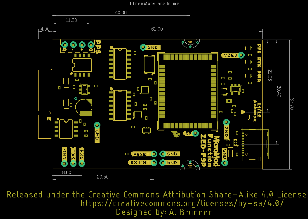
Board Dimensions
The board matches the MicroMod Function Board design specifications and measures 2.56" x 1.48" (65.02mm x 37.69mm) and the USB-C connector protrudes roughly 0.067" (1.70mm) from the edge of the board.