MicroMod GNSS Carrier Board (ZED-F9P) Hookup Guide
 bboyho,
  Elias The Sparkiest
 Hardware Overview
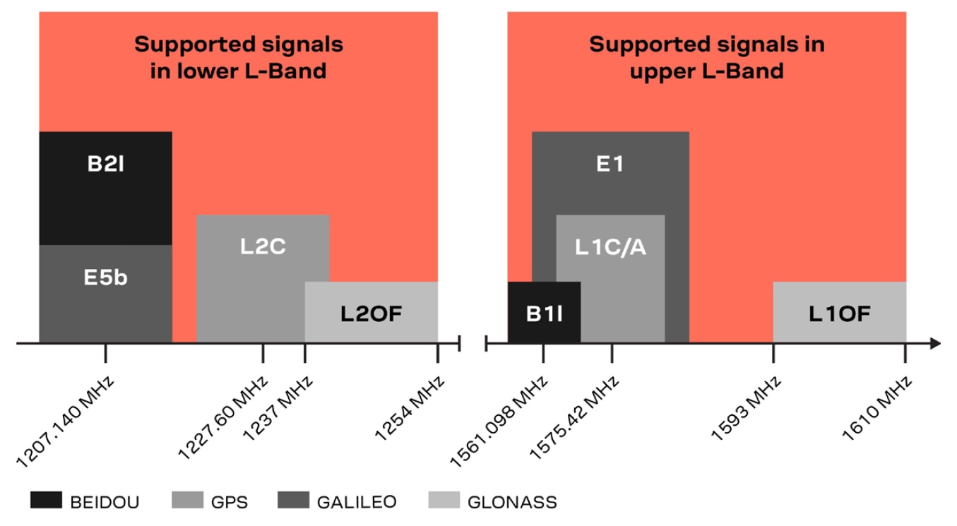
One of the key differentiators between the ZED-F9P and almost all other low-cost RTK solutions is the ZED-F9P is capable of receiving both L1 and L2 bands.
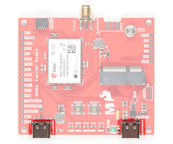
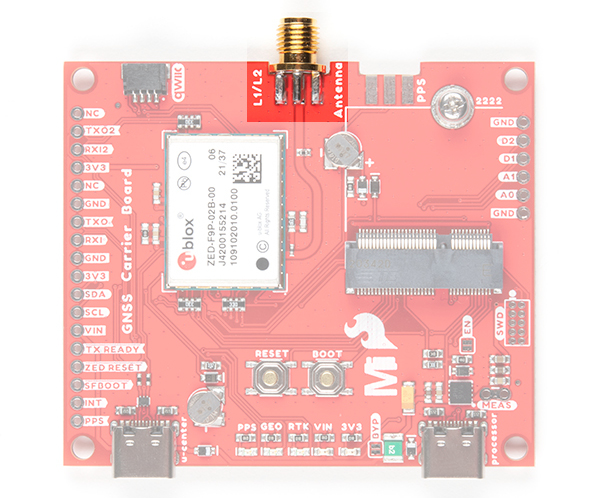
MicroMod Processor Board Socket
The MicroMod GNSS Carrier Board (ZED-F9P) includes a location for a MicroMod Processor Board. Here is where your chosen Processor Board will reside.
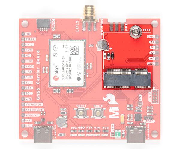
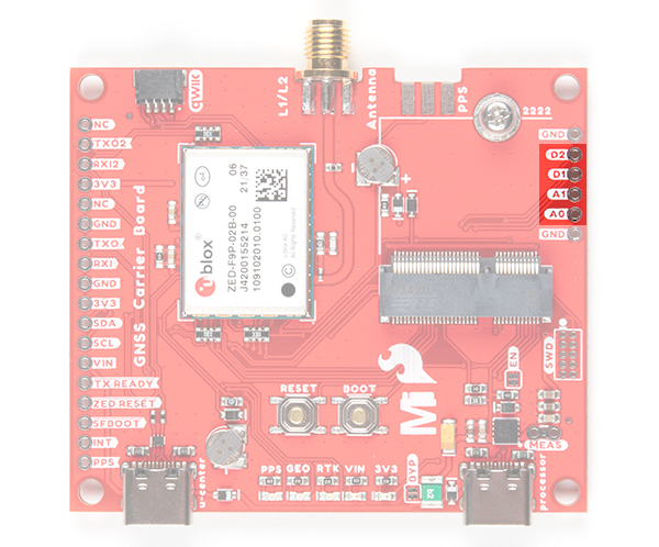
MicroMod Processor General Pins
Next to the MicroMod Processor Board are extra pins if you need to use a digital or analog pin.
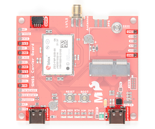
Power
There are a few ways to power the board. Voltage is regulated down to 3.3V with the AP7361 voltage regulator. The square IC next to the USB C labeled as processor is where you will find the AP7361.
- USB C Connector - You can connect a USB Type C cable from your computer's USB port to the board through either of the USB Type C connectors labeled as u-center and processor. There are protection diodes connected to the voltage lines so you can connect two USB cables at the same time to power the board. The AP7361 voltage regulator will regulate the 5V from the USB port down to 3.3V for the system voltage.
- VIN - If you decide to connect to the VIN pin, we recommend a voltage between 3.3V to 6.0V. The AP7361 voltage regulator will regulate the voltage down to 3.3V for the system voltage.
- 3V3 - If you decide to power the board through the 3.3V pin, you could connect a regulated 3.3V to this pin. Otherwise, you could use this to power any peripherals attached to the board.
- Qwiic Connector - The Qwiic connector connects to 3.3V and GND to power any Qwiic-enabled devices. Depending on your application, you could connect a regulated 3.3V through this port as well.
- GND - Of course, you'll need to connect the ground plane to your power source. This pin is available should you decide to power the board through the any of the PTH pins.
Backup Batteries
There are two built-in backup batteries (ML414H) on the board. The backup battery has a 1mAh capacity and requires 20 minute to charge. The battery near the SMA connector is for the Processor Board's RTC and helps keep the RTC running when the external power is removed. Depending on the processor, it may not be connected.
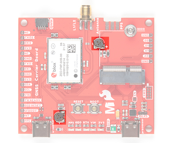
The other one that is closest to the USB C connector labeled as u-center is for the ZED-F9P module. The rechargeable battery maintains the battery backed RAM (BBR) on the GNSS module. This allows for much faster position locks (a.k.a. hot start). The BBR is also used for module configuration retention. The battery is automatically trickle charged when power is applied and should maintain settings and GNSS orbit data for up to two weeks without power.
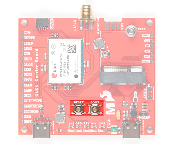
Reset and Boot Buttons
The reset button will reset the processor. The boot button will put the processor into a special boot mode. Depending on the processor board, this boot pin may not be connected.
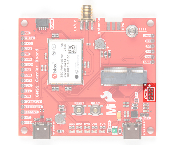
SWD Programming Pins
For advanced users, we broke out the SWD programming pins to connect to a MicroMod Processor Board. Note that this is not populated so you will need a compatible header and compatible JTAG programmer to connect.
Communication Ports
The ZED-F9P is unique in that it has five communication ports which are all active simultaneously. You can read NMEA data over I2C while you send configuration commands over the UART and vice/versa. The only limit is that the SPI pins are mapped onto the I2C and UART pins so it’s either SPI or I2C+UART. The USB port is available at all times.
USB
As stated earlier, there are two USB ports: one for u-center and another for processor. The USB C connector labeled as u-center makes it easy to connect the ZED-F9P to u-center for configuration and quick viewing of NMEA sentences. It is also possible to connect a Raspberry Pi or other single board computer over USB. The ZED-F9P enumerates as a serial COM port and it is a separate serial port from the UART interface. See Getting Started with U-Center for more information about getting the USB port to be a serial COM port. The USB connector labeled as processor is available to program your MicroMod Processor Board. Make sure to check your respective Processor Board to install the USB-to-serial drivers.
A 3.3V regulator is provided to regulate the 5V USB down to 3.3V the module requires. External 5V can be applied or a direct feed of 3.3V can be provided. Note that if you’re provide the board with 3.3V directly it should be a clean supply with minimal noise (less than 50mV VPP ripple is ideal for precision locating).
The 3.3V regulator is capable of sourcing 600mA from a 5V input and the USB C connection is capable of sourcing 2A.
I2C (a.k.a DDC)
The u-blox ZED-F9P has a “DDC” port which is really just an I2C port (without all the fuss of trademark issues). These pins are shared with the SPI pins. By default, the I2C pins are enabled. Be sure the SPI jumper on the rear of the board is open. The MicroMod GNSS Carrier Board also includes one Qwiic connector to make daisy chaining this GPS receiver with a large variety of I2C devices. Checkout Qwiic for your next project.
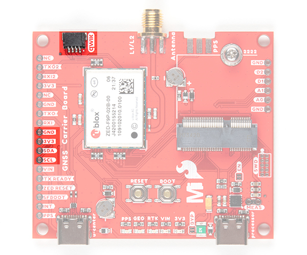
UART/Serial
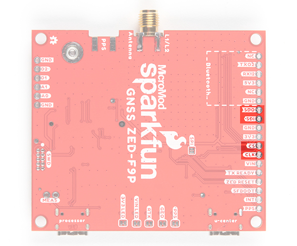
The classic serial pins are available on the ZED-F9P but are shared with the SPI pins. By default, the UART pins are enabled. Be sure the SPI jumper on the rear of the board is open.
- TXO/SDO = TX out from ZED-F9P
- RXI/SDI = RX into ZED-F9P
 |
 |
| Top View | Bottom View |
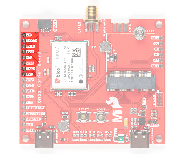
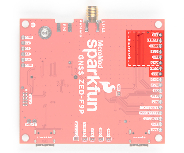
There is a second serial port (UART2) available on the ZED-F9P that is primarily used for RTCM3 correction data. By default, this port will automatically receive and parse incoming RTCM3 strings enabling RTK mode on the board. In addition to the TXO2/RXI2 pins we have added an additional ‘RTCM Correction’ port where we arranged the pins to match the industry standard serial connection (aka the 'FTDI' pinout). While we label this as "Bluetooth" on the back of the board, you can still connect any transceiver or serial-to-USB converter to this port. This pinout is compatible with our Bluetooth Mate and Serial Basic so you can send RTCM correction data from a cell phone or computer. Note that RTCM3 data can also be sent over I2C, UART1, SPI, or USB if desired.
The RTCM correction port (UART2) defaults to 38400bps serial but can be configured via software commands (checkout our Arduino library) or over USB using u-center. Keep in mind our Bluetooth Mate defaults to 115200bps. If you plan to use Bluetooth for correction data (we found it to be easiest), we recommend you increase this port speed to 115200bps using u-center. Additionally, but less often needed, the UART2 can be configured for NMEA output. In general, we don’t use UART2 for anything but RTCM correction data, so we recommend leaving the in/out protocols as RTCM.

If you’ve got the ZED-F9P setup for base station mode (also called survey-in mode) the UART2 will output RTCM3 correction data. This means you can connect a radio or wired link to UART2 and the board will automatically send just RTCM bytes over the link (no NMEA data taking up bandwidth).
SPI
The ZED-F9P can also be configured for SPI communication. By default, the SPI port is disabled. To enable SPI close the SPI jumper on the rear of the board. Closing this jumper will disable the UART1 and I2C interfaces (UART2 will continue to operate as normal).
Antenna
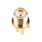
The ZED-F9P requires a good quality GPS or GNSS (preferred) antenna. For a secure connection, we include an SMA female connector. To make the most out of the ZED-F9P, you'll need a multi-band GNSS antenna and an SMA male connector to mate.
Low-cost magnetic GPS/GNSS antennas can be used (checkout the u-blox white paper) but a 4” / 10cm metal disc is required to be placed under the antenna as a metal ground plane.
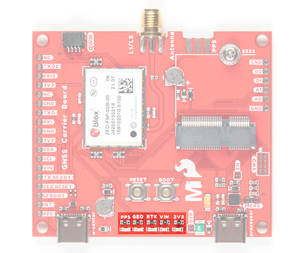
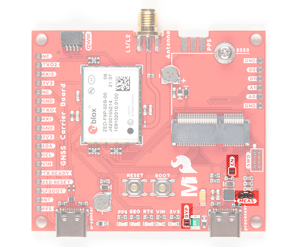
LEDs
The board includes five status LEDs as indicated in the image below.
- PPS: The pulse per second LED will illuminate each second once a position lock has been achieved.
- GEO: The GEO LED can be configured to turn on/off for geofencing applications.
- RTK: The RTK LED will be illuminated constantly upon power up. Once RTCM data has been successfully received it will begin to blink. This is a good way to see if the ZED-F9P is getting RTCM from various sources. Once an RTK fix is obtained, the LED will turn off.
- VIN: The VIN LED will illuminate when there is voltage applied to the VIN pin or over USB.
- 3V3: The power LED will illuminate when 3.3V is activated either over USB or via the Qwiic bus.
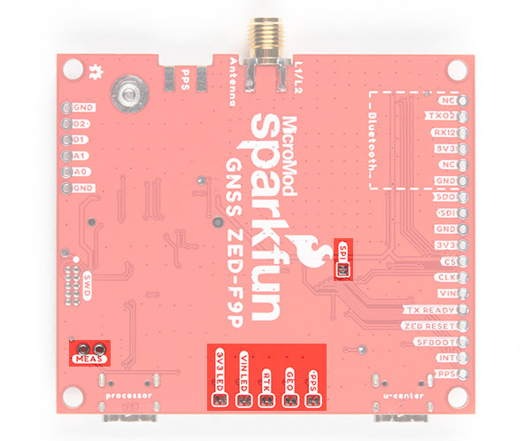
Jumpers
There are jumpers located throughout the board. Below are the jumpers on the top side of the board.
- Bypass (BYP): By default, the BYP is left open. Adding a solder jumper bypasses the 2A resettable fuse on the back of the board should you decide to pull more than 2A from your USB source. Proceed with caution should you decide to bypass the jumper.
- Enable (EN): By default, the EN jumper is left open. This jumper is connected to a processor board's GPIO pin. The processor board can control the ATP's voltage regulator. Depending on the processor, this may not be connected.
- Current Measurement (MEAS): By default, the MEAS is closed. Cutting the jumper and soldering to the PTH pads will allows you to insert a current meter and precisely monitor the how much current your application is consuming.
Below are the jumpers on the bottom side of the board.
- 3V3 LED: By default, the 3V3 LED is closed. Cutting this jumper will disable the LED when there is 3.3V.
- VIN LED: By default, the VIN LED is closed. Cutting this jumper will disable the LED whenever there is an input voltage.
- RTK: By default, the RTK is closed. Cutting this jumper will disable the RTK LED. This LED indicates when there is an RTK fix.
- GEO: By default, the GEO is closed. Cutting this jumper will disable the GEO LED. This LED is used for geofencing applications.
- PPS: By default, the PPS is closed. Cutting this jumper will disable the PPS LED whenever a position lock has been achieved.
- SPI: By default, the SPI is open. Closing SPI with solder enables the SPI interface and disables the UART and I2C interfaces. USB will still function.
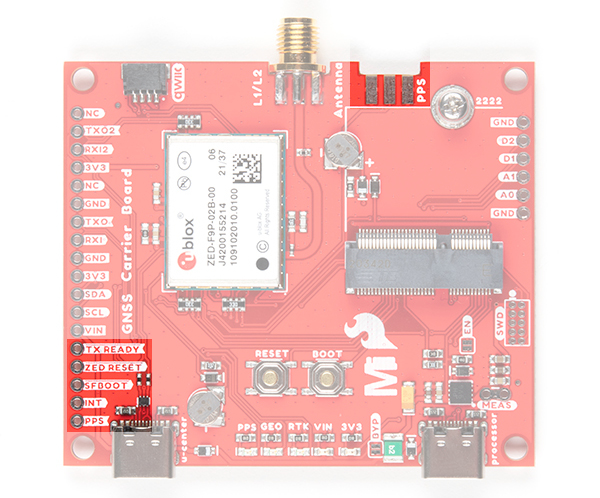
Control Pins
These pins are used for various extra control of the ZED-F9P:
- TX READY: Transmit ready output pin. Can be configured using U-Center to indicate that the transmit buffer is full and ready to be transmitted. This is connected to D0 on the MicroMod Processor Board.
- ZED RESET: Reset input pin. Pull this line low to reset the module.
- SFBOOT: Safeboot input pin. This is required for firmware updates to the module and generally should not be used or connected.
- INT: Interrupt input/output pin. Can be configured using U-Center to bring the module out of deep sleep or to output an interrupt for various module states.
- PPS: Pulse-per-second output pin. Begins blinking at 1Hz when module gets basic GPS/GNSS position lock.
Hardware Pinout
| AUDIO | UART | GPIO/BUS | I2C | SDIO | SPI | Dedicated |
| Function | Bottom Pin |
Top Pin |
Function | ||||||
|---|---|---|---|---|---|---|---|---|---|
| (Not Connected) | 75 | GND | |||||||
| 3.3V | 74 | 73 | G5 / BUS5 | ||||||
| RTC_3V_BATT | 72 | 71 | G6 / BUS6 | ||||||
| SPI_CS1# | SDIO_DATA3 (I/O) | 70 | 69 | G7 / BUS7 | |||||
| SDIO_DATA2 (I/O) | 68 | 67 | G8 | ||||||
| SDIO_DATA1 (I/O) | 66 | 65 | G9 | ADC_D- | CAM_HSYNC | ||||
| SPI_CIPO1 | SDIO_DATA0 (I/O) | 64 | 63 | G10 | ADC_D+ | CAM_VSYNC | |||
| SPI COPI1 | SDIO_CMD (I/O) | 62 | 61 | SPI_CIPO (I) | |||||
| SPI SCK1 | SDIO_SCK (O) | 60 | 59 | SPI_COPI (O) | LED_DAT | ||||
| AUD_MCLK (O) | 58 | 57 | SPI_SCK (O) | LED_CLK | |||||
| CAM_MCLK | PCM_OUT | I2S_OUT | AUD_OUT | 56 | 55 | SPI_CS# | |||
| CAM_PCLK | PCM_IN | I2S_IN | AUD_IN | 54 | 53 | I2C_SCL1 (I/O) | |||
| PDM_DATA | PCM_SYNC | I2S_WS | AUD_LRCLK | 52 | 51 | I2C_SDA1 (I/O) | |||
| PDM_CLK | PCM_CLK | I2S_SCK | AUD_BCLK | 50 | 49 | BATT_VIN / 3 (I - ADC) (0 to 3.3V) | |||
| G4 / BUS4 | 48 | 47 | PWM1 | ||||||
| G3 / BUS3 | 46 | 45 | GND | ||||||
| G2 / BUS2 | 44 | 43 | CAN_TX | ||||||
| G1 / BUS1 | 42 | 41 | CAN_RX | ||||||
| G0 / BUS0 | 40 | 39 | GND | ||||||
| A1 | 38 | 37 | USBHOST_D- | ||||||
| GND | 36 | 35 | USBHOST_D+ | ||||||
| A0 | 34 | 33 | GND | ||||||
| PWM0 | 32 | 31 | Module Key | ||||||
| Module Key | 30 | 29 | Module Key | ||||||
| Module Key | 28 | 27 | Module Key | ||||||
| Module Key | 26 | 25 | Module Key | ||||||
| Module Key | 24 | 23 | SWDIO | ||||||
| UART_TX2 (O) | 22 | 21 | SWDCK | ||||||
| UART_RX2 (I) | 20 | 19 | UART_RX1 (I) | ||||||
| CAM_TRIG | D1 | 18 | 17 | UART_TX1 (0) | |||||
| I2C_INT# | 16 | 15 | UART_CTS1 (I) | ||||||
| I2C_SCL (I/0) | 14 | 13 | UART_RTS1 (O) | ||||||
| I2C_SDA (I/0) | 12 | 11 | BOOT (I - Open Drain) | ||||||
| D0 | 10 | 9 | USB_VIN | ||||||
| SWO | G11 | 8 | 7 | GND | |||||
| RESET# (I - Open Drain) | 6 | 5 | USB_D- | ||||||
| 3.3V_EN | 4 | 3 | USB_D+ | ||||||
| 3.3V | 2 | 1 | GND | ||||||
| Function | Bottom Pin |
Top Pin |
Function | ||
|---|---|---|---|---|---|
| (Not Connected) | 75 | GND | |||
| 3.3V | 74 | 73 | |||
| RTC_3V | 72 | 71 | |||
| 70 | 69 | ||||
| 66 | 65 | ||||
| 64 | 63 | ||||
| 62 | 61 | TXO | SDO | ||
| 60 | 59 | RXI | SDI | ||
| 58 | 57 | SCL | SCK | ||
| 56 | 55 | SDA | CS | ||
| 54 | 53 | ||||
| 52 | 51 | ||||
| 50 | 49 | VIN/3 | |||
| 48 | 47 | ||||
| 46 | 45 | GND | |||
| 44 | 43 | ||||
| 42 | 41 | ||||
| D2 | G0 | 40 | 39 | GND | |
| A1 | 38 | 37 | |||
| GND | 36 | 35 | |||
| A0 | 34 | 33 | GND | ||
| 32 | 31 | ||||
| 30 | 29 | ||||
| 28 | 27 | ||||
| 26 | 25 | ||||
| 24 | 23 | SWDIO | |||
| RXI2 | 22 | 21 | SWDCK | ||
| TXO2 | 20 | 19 | TXO | SDO | |
| D1 | 18 | 17 | RXI | SDI | |
| INT | 16 | 15 | |||
| SCK | SCL | 14 | 13 | ||
| CS | SDA | 12 | 11 | BOOT | |
| TX_READY | 10 | 9 | VIN | ||
| 8 | 7 | GND | |||
| RESET | 6 | 5 | USB_D- | ||
| 3.3V_EN | 4 | 3 | USB_D+ | ||
| 3.3V | 2 | 1 | GND | ||
| Signal Group | Signal | I/O | Description | Voltage | Power | 3.3V | I | 3.3V Source | 3.3V |
|---|---|---|---|---|
| GND | Return current path | 0V | ||
| USB_VIN | I | USB VIN compliant to USB 2.0 specification. Connect to pins on processor board that require 5V for USB functionality | 4.8-5.2V | |
| RTC_3V_BATT | I | 3V provided by external coin cell or mini battery. Max draw=100μA. Connect to pins maintaining an RTC during power loss. Can be left NC. | 3V | |
| 3.3V_EN | O | Controls the carrier board's main voltage regulator. Voltage above 1V will enable 3.3V power path. | 3.3V | |
| BATT_VIN/3 | I | Carrier board raw voltage over 3. 1/3 resistor divider is implemented on carrier board. Amplify the analog signal as needed for full 0-3.3V range | 3.3V | |
| Reset | Reset | I | Input to processor. Open drain with pullup on processor board. Pulling low resets processor. | 3.3V |
| Boot | I | Input to processor. Open drain with pullup on processor board. Pulling low puts processor into special boot mode. Can be left NC. | 3.3V | |
| USB | USB_D± | I/O | USB Data ±. Differential serial data interface compliant to USB 2.0 specification. If UART is required for programming, USB± must be routed to a USB-to-serial conversion IC on the processor board. | |
| USB Host | USBHOST_D± | I/O | For processors that support USB Host Mode. USB Data±. Differential serial data interface compliant to USB 2.0 specification. Can be left NC. | |
| CAN | CAN_RX | I | CAN Bus receive data. | 3.3V |
| CAN_TX | O | CAN Bus transmit data. | 3.3V | |
| UART | UART_RX1 | I | UART receive data. | 3.3V |
| UART_TX1 | O | UART transmit data. | 3.3V | |
| UART_RTS1 | O | UART ready to send. | 3.3V | |
| UART_CTS1 | I | UART clear to send. | 3.3V | |
| UART_RX2 | I | 2nd UART receive data. | 3.3V | |
| UART_TX2 | O | 2nd UART transmit data. | 3.3V | |
| I2C | I2C_SCL | I/O | I2C clock. Open drain with pullup on carrier board. | 3.3V |
| I2C_SDA | I/O | I2C data. Open drain with pullup on carrier board | 3.3V | |
| I2C_INT# | I | Interrupt notification from carrier board to processor. Open drain with pullup on carrier board. Active LOW | 3.3V | |
| I2C_SCL1 | I/O | 2nd I2C clock. Open drain with pullup on carrier board. | 3.3V | |
| I2C_SDA1 | I/O | 2nd I2C data. Open drain with pullup on carrier board. | 3.3V | |
| SPI | SPI_COPI | O | SPI Controller Output/Peripheral Input. | 3.3V |
| SPI_CIPO | I | SPI Controller Input/Peripheral Output. | 3.3V | |
| SPI_SCK | O | SPI Clock. | 3.3V | |
| SPI_CS# | O | SPI Chip Select. Active LOW. Can be routed to GPIO if hardware CS is unused. | 3.3V | |
| SPI/SDIO | SPI_SCK1/SDIO_CLK | O | 2nd SPI Clock. Secondary use is SDIO Clock. | 3.3V |
| SPI_COPI1/SDIO_CMD | I/O | 2nd SPI Controller Output/Peripheral Input. Secondary use is SDIO command interface. | 3.3V | |
| SPI_CIPO1/SDIO_DATA0 | I/O | 2nd SPI Peripheral Input/Controller Output. Secondary use is SDIO data exchange bit 0. | 3.3V | |
| SDIO_DATA1 | I/O | SDIO data exchange bit 1. | 3.3V | |
| SDIO_DATA2 | I/O | SDIO data exchange bit 2. | 3.3V | |
| SPI_CS1/SDIO_DATA3 | I/O | 2nd SPI Chip Select. Secondary use is SDIO data exchange bit 3. | 3.3V | |
| Audio | AUD_MCLK | O | Audio master clock. | 3.3V |
| AUD_OUT/PCM_OUT/I2S_OUT/CAM_MCLK | O | Audio data output. PCM synchronous data output. I2S serial data out. Camera master clock. | 3.3V | |
| AUD_IN/PCM_IN/I2S_IN/CAM_PCLK | I | Audio data input. PCM syncrhonous data input. I2S serial data in. Camera periphperal clock. | 3.3V | |
| AUD_LRCLK/PCM_SYNC/I2S_WS/PDM_DATA | I/O | Audio left/right clock. PCM syncrhonous data SYNC. I2S word select. PDM data. | 3.3V | |
| AUD_BCLK/PCM_CLK/I2S_CLK/PDM_CLK | O | Audio bit clock. PCM clock. I2S continuous serial clock. PDM clock. | 3.3V | |
| SWD | SWDIO | I/O | Serial Wire Debug I/O. Connect if processor board supports SWD. Can be left NC. | 3.3V |
| SWDCK | I | Serial Wire Debug clock. Connect if processor board supports SWD. Can be left NC. | 3.3V | |
| ADC | A0 | I | Analog to digital converter 0. Amplify the analog signal as needed to enable full 0-3.3V range. | 3.3V |
| A1 | I | Analog to digital converter 1. Amplify the analog signal as needed to enable full 0-3.3V range. | 3.3V | |
| PWM | PWM0 | O | Pulse width modulated output 0. | 3.3V |
| PWM1 | O | Pulse width modulated output 1. | 3.3V | |
| Digital | D0 | I/O | General digital input/output pin. | 3.3V |
| D1/CAM_TRIG | I/O | General digital input/output pin. Camera trigger. | 3.3V | |
| General/Bus | G0/BUS0 | I/O | General purpose pins. Any unused processor pins should be assigned to Gx with ADC + PWM capable pins given priority (0, 1, 2, etc.) positions. The intent is to guarantee PWM, ADC and Digital Pin functionality on respective ADC/PWM/Digital pins. Gx pins do not guarantee ADC/PWM function. Alternative use is pins can support a fast read/write 8-bit or 4-bit wide bus. | 3.3V |
| G1/BUS1 | I/O | 3.3V | ||
| G2/BUS2 | I/O | 3.3V | ||
| G3/BUS3 | I/O | 3.3V | ||
| G4/BUS4 | I/O | 3.3V | ||
| G5/BUS5 | I/O | 3.3V | ||
| G6/BUS6 | I/O | 3.3V | ||
| G7/BUS7 | I/O | 3.3V | ||
| G8 | I/O | General purpose pin | 3.3V | |
| G9/ADC_D-/CAM_HSYNC | I/O | Differential ADC input if available. Camera horizontal sync. | 3.3V | |
| G10/ADC_D+/CAM_VSYNC | I/O | Differential ADC input if available. Camera vertical sync. | 3.3V | |
| G11/SWO | I/O | General purpose pin. Serial Wire Output | 3.3V |
Board Dimension
The board is about 2.24"x2.60" and includes four mounting holes on each corner. If you include the length of the connectors sticking out from the edge of the board, the overall size of the board is about 2.52"x2.60".
