MicroMod Artemis Processor Board Hookup Guide
 Nate, Ell C
Hardware Overview
While the Artemis module is pretty self-contained, let's have a look at a few of the unique features of this MicroMod Processor Board.
Power
Power is supplied by the carrier board, but it should be noted that all pins are 3.3V.
The ADC on the Artemis is 0-2V. Exposing an ADC pin to 3.3V will not harm the device but the ADC will saturate returning 16,383 (14-bit) for voltages greater than 2V.
M.2 Connector
All of our MicroMod Processor boards come equipped with the M.2 MicroMod Connector, which leverages the M.2 standard and specification to allow you to install your MicroMod Processor board on your choice of carrier board.
 |
 |
| M.2 Connector from the Front | M.2 Connector from the Back |
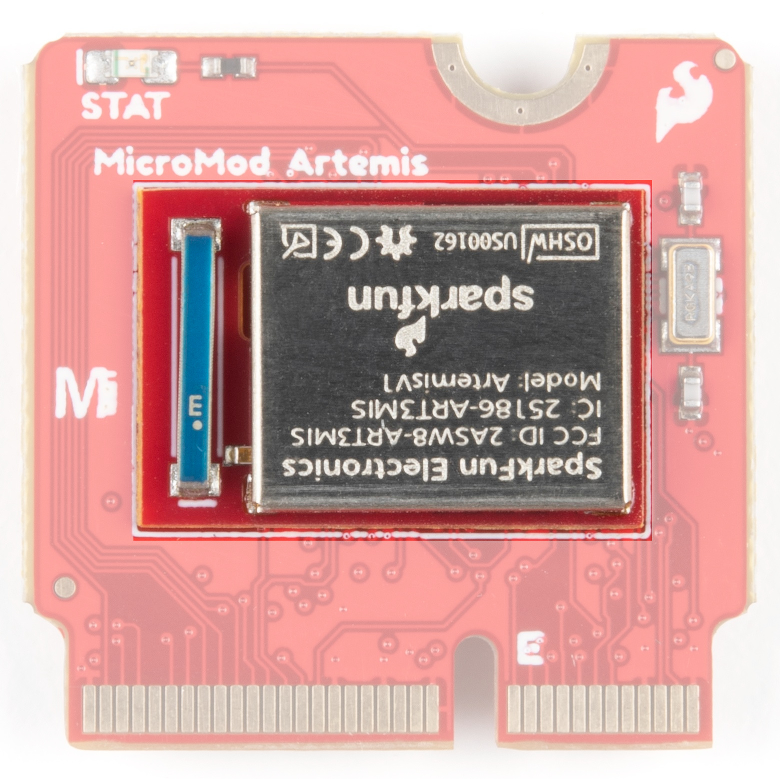
Artemis Processor
The SparkFun Artemis Processor provides a Cortex-M4F with BLE 5.0 running up to 96MHz and with as low power as 6uA per MHz (less than 5mW). This module is powerful enough to run TensorFlow, Machine Learning, and all sorts of voice recognition software. A deep dive into all of Artemis's delightful features can be found in the Designing with the SparkFun Artemis tutorial.
Op Amp
Incoming analog voltages over 2V will saturate the Artemis's analog to digital converter. We've integrated an OpAmp to scale the incoming 0-3.3V voltages down to the 0-2V range that the Artemis can handle.

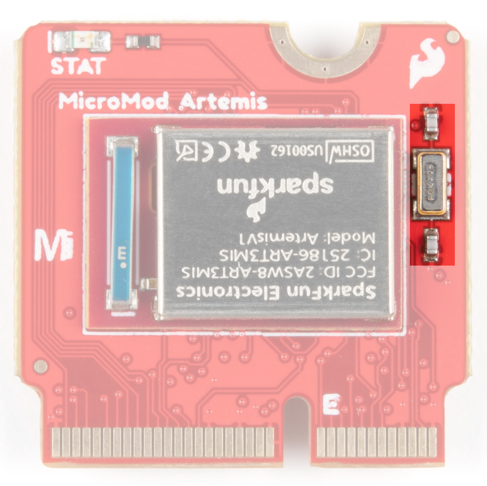
RTC
An onboard RTC crystal has been integrated.
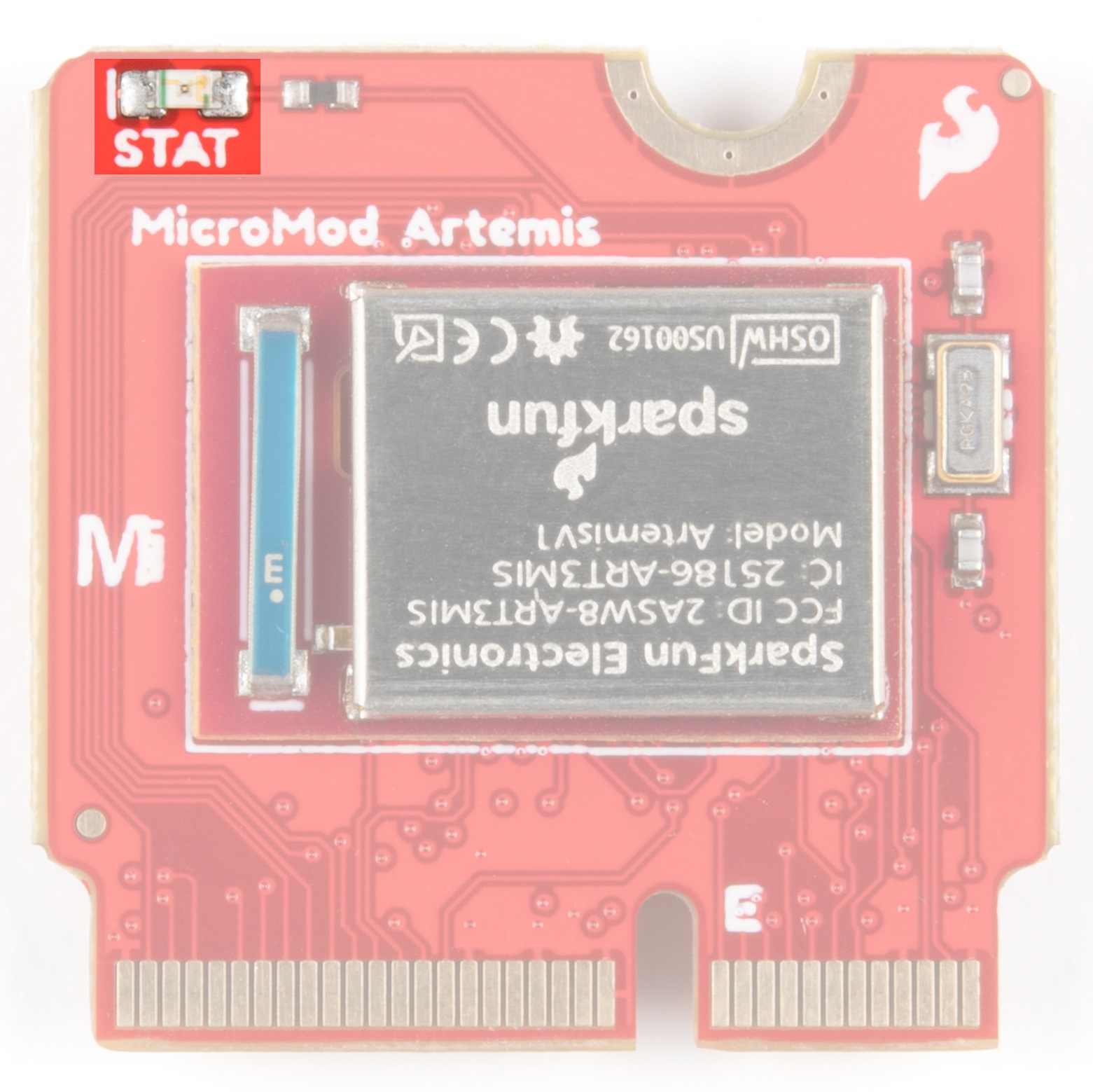
Status LED
We've also included a Status LED for all your blinky needs.
Artemis MicroMod Processor Pin Functionality
| AUDIO | UART | GPIO/BUS | I2C | SDIO | SPI | Dedicated |
| Function | Bottom Pin |
Top Pin |
Function | ||||||
|---|---|---|---|---|---|---|---|---|---|
| (Not Connected) | 75 | GND | |||||||
| 3.3V | 74 | 73 | G5 / BUS5 | ||||||
| RTC_3V_BATT | 72 | 71 | G6 / BUS6 | ||||||
| SPI_CS1# | SDIO_DATA3 (I/O) | 70 | 69 | G7 / BUS7 | |||||
| SDIO_DATA2 (I/O) | 68 | 67 | G8 | ||||||
| SDIO_DATA1 (I/O) | 66 | 65 | G9 | ADC_D- | CAM_HSYNC | ||||
| SPI_CIPO1 | SDIO_DATA0 (I/O) | 64 | 63 | G10 | ADC_D+ | CAM_VSYNC | |||
| SPI COPI1 | SDIO_CMD (I/O) | 62 | 61 | SPI_CIPO (I) | |||||
| SPI SCK1 | SDIO_SCK (O) | 60 | 59 | SPI_COPI (O) | LED_DAT | ||||
| AUD_MCLK (O) | 58 | 57 | SPI_SCK (O) | LED_CLK | |||||
| CAM_MCLK | PCM_OUT | I2S_OUT | AUD_OUT | 56 | 55 | SPI_CS# | |||
| CAM_PCLK | PCM_IN | I2S_IN | AUD_IN | 54 | 53 | I2C_SCL1 (I/O) | |||
| PDM_DATA | PCM_SYNC | I2S_WS | AUD_LRCLK | 52 | 51 | I2C_SDA1 (I/O) | |||
| PDM_CLK | PCM_CLK | I2S_SCK | AUD_BCLK | 50 | 49 | BATT_VIN / 3 (I - ADC) (0 to 3.3V) | |||
| G4 / BUS4 | 48 | 47 | PWM1 | ||||||
| G3 / BUS3 | 46 | 45 | GND | ||||||
| G2 / BUS2 | 44 | 43 | CAN_TX | ||||||
| G1 / BUS1 | 42 | 41 | CAN_RX | ||||||
| G0 / BUS0 | 40 | 39 | GND | ||||||
| A1 | 38 | 37 | USBHOST_D- | ||||||
| GND | 36 | 35 | USBHOST_D+ | ||||||
| A0 | 34 | 33 | GND | ||||||
| PWM0 | 32 | 31 | Module Key | ||||||
| Module Key | 30 | 29 | Module Key | ||||||
| Module Key | 28 | 27 | Module Key | ||||||
| Module Key | 26 | 25 | Module Key | ||||||
| Module Key | 24 | 23 | SWDIO | ||||||
| UART_TX2 (O) | 22 | 21 | SWDCK | ||||||
| UART_RX2 (I) | 20 | 19 | UART_RX1 (I) | ||||||
| CAM_TRIG | D1 | 18 | 17 | UART_TX1 (0) | |||||
| I2C_INT# | 16 | 15 | UART_CTS1 (I) | ||||||
| I2C_SCL (I/0) | 14 | 13 | UART_RTS1 (O) | ||||||
| I2C_SDA (I/0) | 12 | 11 | BOOT (I - Open Drain) | ||||||
| D0 | 10 | 9 | USB_VIN | ||||||
| SWO | G11 | 8 | 7 | GND | |||||
| RESET# (I - Open Drain) | 6 | 5 | USB_D- | ||||||
| 3.3V_EN | 4 | 3 | USB_D+ | ||||||
| 3.3V | 2 | 1 | GND | ||||||
| Artemis Pin |
Alternate Function |
Primary Function |
Bottom Pin |
Top Pin |
Primary Function |
Alternate Function |
Artemis Pin |
|---|---|---|---|---|---|---|---|
| (Not Connected) | 73 | G5 | A29 | ||||
| - | 72 | 71 | G6 | D14 | |||
| D23 | QSPI3 | SPI_CS1 | 70 | 69 | G7 | D15 | |
| D4 | QSPI2 | 68 | 67 | - | |||
| D26 | QSPI1 | 66 | 65 | TX1 | ADC_D- | A12 | |
| D6 | QSPI0 | SPI_CIPO1 | 64 | 63 | ADC_D+ | A13 | |
| D7 | QSPI_CS | SPI_COPI1 | 62 | 61 | SPI_CIPO | D43 | |
| D5 | QSPI_SCK | SPI_SCK1 | 60 | 59 | SPI_COPI | D38 | |
| D18 | CAM_MCLK | 58 | 57 | SPI_SCK | D42 | ||
| D18 | CAM_MCLK | 56 | 55 | SPI_CS | D41 | ||
| A11 | CAM_PCLK | 54 | 53 | SCL1 | D8 | ||
| D36 | PDM_DATA | 52 | 51 | SDA1 | D9 | ||
| D37 | PDM_CLK | 50 | 49 | BATT_VIN / 3 | A31 | ||
| D28 | G4 | 48 | 47 | PWM1 | D45 | ||
| D27 | G3 | 46 | 45 | - | |||
| A34 | G2 | 44 | 43 | - | |||
| A33 | G1 | 42 | 41 | - | |||
| A16 | G0 | 40 | 39 | GND | |||
| A35 | ADC1 | 38 | 37 | - | |||
| A32 | ADC0 | 34 | 33 | - | |||
| D44 | PWM0 | 32 | 31 | - | |||
| - | 24 | 23 | SWDIO | D21 | |||
| - | 22 | 21 | SWDCK | D20 | |||
| - | 20 | 19 | RX1 | D25 | |||
| D1 | D1 | 18 | 17 | TX1 | ADC_D- | A12 | |
| D2 | I2C_Interrupt | 16 | 15 | CTS1 | D17 | ||
| D39 | SCL | 14 | 13 | RTS1 | D10 | ||
| D40 | SDA | 12 | 11 | BOOT | |||
| D0 | D0 | 10 | 9 | - | |||
| - | 8 | 7 | GND | ||||
| RESET | 6 | 5 | USB_D- | ||||
| - | 4 | 3 | USB_D+ | ||||
| 3.3V | 2 | 1 | GND |
| Signal Group | Signal | I/O | Description | Voltage | Power | 3.3V | I | 3.3V Source | 3.3V |
|---|---|---|---|---|
| GND | Return current path | 0V | ||
| USB_VIN | I | USB VIN compliant to USB 2.0 specification. Connect to pins on processor board that require 5V for USB functionality | 4.8-5.2V | |
| RTC_3V_BATT | I | 3V provided by external coin cell or mini battery. Max draw=100μA. Connect to pins maintaining an RTC during power loss. Can be left NC. | 3V | |
| 3.3V_EN | O | Controls the carrier board's main voltage regulator. Voltage above 1V will enable 3.3V power path. | 3.3V | |
| BATT_VIN/3 | I | Carrier board raw voltage over 3. 1/3 resistor divider is implemented on carrier board. Amplify the analog signal as needed for full 0-3.3V range | 3.3V | |
| Reset | Reset | I | Input to processor. Open drain with pullup on processor board. Pulling low resets processor. | 3.3V |
| Boot | I | Input to processor. Open drain with pullup on processor board. Pulling low puts processor into special boot mode. Can be left NC. | 3.3V | |
| USB | USB_D± | I/O | USB Data ±. Differential serial data interface compliant to USB 2.0 specification. If UART is required for programming, USB± must be routed to a USB-to-serial conversion IC on the processor board. | |
| USB Host | USBHOST_D± | I/O | For processors that support USB Host Mode. USB Data±. Differential serial data interface compliant to USB 2.0 specification. Can be left NC. | |
| CAN | CAN_RX | I | CAN Bus receive data. | 3.3V |
| CAN_TX | O | CAN Bus transmit data. | 3.3V | |
| UART | UART_RX1 | I | UART receive data. | 3.3V |
| UART_TX1 | O | UART transmit data. | 3.3V | |
| UART_RTS1 | O | UART ready to send. | 3.3V | |
| UART_CTS1 | I | UART clear to send. | 3.3V | |
| UART_RX2 | I | 2nd UART receive data. | 3.3V | |
| UART_TX2 | O | 2nd UART transmit data. | 3.3V | |
| I2C | I2C_SCL | I/O | I2C clock. Open drain with pullup on carrier board. | 3.3V |
| I2C_SDA | I/O | I2C data. Open drain with pullup on carrier board | 3.3V | |
| I2C_INT# | I | Interrupt notification from carrier board to processor. Open drain with pullup on carrier board. Active LOW | 3.3V | |
| I2C_SCL1 | I/O | 2nd I2C clock. Open drain with pullup on carrier board. | 3.3V | |
| I2C_SDA1 | I/O | 2nd I2C data. Open drain with pullup on carrier board. | 3.3V | |
| SPI | SPI_COPI | O | SPI Controller Output/Peripheral Input. | 3.3V |
| SPI_CIPO | I | SPI Controller Input/Peripheral Output. | 3.3V | |
| SPI_SCK | O | SPI Clock. | 3.3V | |
| SPI_CS# | O | SPI Chip Select. Active LOW. Can be routed to GPIO if hardware CS is unused. | 3.3V | |
| SPI/SDIO | SPI_SCK1/SDIO_CLK | O | 2nd SPI Clock. Secondary use is SDIO Clock. | 3.3V |
| SPI_COPI1/SDIO_CMD | I/O | 2nd SPI Controller Output/Peripheral Input. Secondary use is SDIO command interface. | 3.3V | |
| SPI_CIPO1/SDIO_DATA0 | I/O | 2nd SPI Peripheral Input/Controller Output. Secondary use is SDIO data exchange bit 0. | 3.3V | |
| SDIO_DATA1 | I/O | SDIO data exchange bit 1. | 3.3V | |
| SDIO_DATA2 | I/O | SDIO data exchange bit 2. | 3.3V | |
| SPI_CS1/SDIO_DATA3 | I/O | 2nd SPI Chip Select. Secondary use is SDIO data exchange bit 3. | 3.3V | |
| Audio | AUD_MCLK | O | Audio master clock. | 3.3V |
| AUD_OUT/PCM_OUT/I2S_OUT/CAM_MCLK | O | Audio data output. PCM synchronous data output. I2S serial data out. Camera master clock. | 3.3V | |
| AUD_IN/PCM_IN/I2S_IN/CAM_PCLK | I | Audio data input. PCM syncrhonous data input. I2S serial data in. Camera periphperal clock. | 3.3V | |
| AUD_LRCLK/PCM_SYNC/I2S_WS/PDM_DATA | I/O | Audio left/right clock. PCM syncrhonous data SYNC. I2S word select. PDM data. | 3.3V | |
| AUD_BCLK/PCM_CLK/I2S_CLK/PDM_CLK | O | Audio bit clock. PCM clock. I2S continuous serial clock. PDM clock. | 3.3V | |
| SWD | SWDIO | I/O | Serial Wire Debug I/O. Connect if processor board supports SWD. Can be left NC. | 3.3V |
| SWDCK | I | Serial Wire Debug clock. Connect if processor board supports SWD. Can be left NC. | 3.3V | |
| ADC | A0 | I | Analog to digital converter 0. Amplify the analog signal as needed to enable full 0-3.3V range. | 3.3V |
| A1 | I | Analog to digital converter 1. Amplify the analog signal as needed to enable full 0-3.3V range. | 3.3V | |
| PWM | PWM0 | O | Pulse width modulated output 0. | 3.3V |
| PWM1 | O | Pulse width modulated output 1. | 3.3V | |
| Digital | D0 | I/O | General digital input/output pin. | 3.3V |
| D1/CAM_TRIG | I/O | General digital input/output pin. Camera trigger. | 3.3V | |
| General/Bus | G0/BUS0 | I/O | General purpose pins. Any unused processor pins should be assigned to Gx with ADC + PWM capable pins given priority (0, 1, 2, etc.) positions. The intent is to guarantee PWM, ADC and Digital Pin functionality on respective ADC/PWM/Digital pins. Gx pins do not guarantee ADC/PWM function. Alternative use is pins can support a fast read/write 8-bit or 4-bit wide bus. | 3.3V |
| G1/BUS1 | I/O | 3.3V | ||
| G2/BUS2 | I/O | 3.3V | ||
| G3/BUS3 | I/O | 3.3V | ||
| G4/BUS4 | I/O | 3.3V | ||
| G5/BUS5 | I/O | 3.3V | ||
| G6/BUS6 | I/O | 3.3V | ||
| G7/BUS7 | I/O | 3.3V | ||
| G8 | I/O | General purpose pin | 3.3V | |
| G9/ADC_D-/CAM_HSYNC | I/O | Differential ADC input if available. Camera horizontal sync. | 3.3V | |
| G10/ADC_D+/CAM_VSYNC | I/O | Differential ADC input if available. Camera vertical sync. | 3.3V | |
| G11/SWO | I/O | General purpose pin. Serial Wire Output | 3.3V |
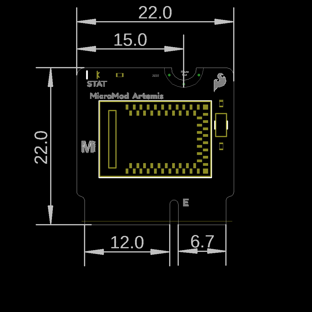
Board Dimensions
The board measures 22mm x 22mm, with 15mm to the top notch and 12mm to the E key. For more information regarding the processor board physical standards, head on over to the Getting Started with MicroMod tutorial and check out the Hardware Overview section.