$20.50
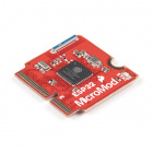
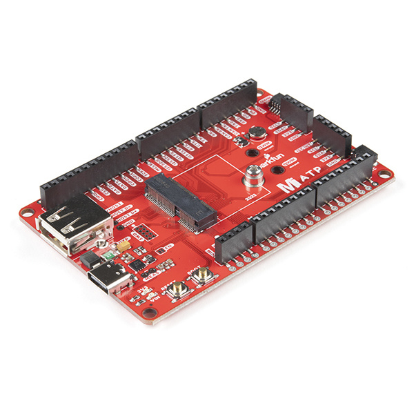
Access All The Pins (i.e. ATP) of the MicroMod Processor Board with the MicroMod ATP Carrier Board!
To follow along with this tutorial, you will need the following materials. You may not need everything though depending on what you have. Add it to your cart, read through the guide, and adjust the cart as necessary.
You'll need a Processor Board with the ATP Carrier Board.
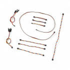
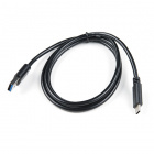
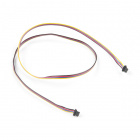
At a minimum, you will need a USB C cable to power and program the boards. Depending on your application, you may want to grab a Qwiic cable to connect a Qwiic-enabled device.
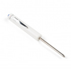
You will need a screw driver to tighten the screw between the processor board and carrier board.
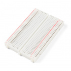
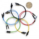
Depending on your setup, you could use jumper wires and a breadboard. However, you will want to strip and solder wires should you decide to solder directly to the plated through holes for a secure connection.
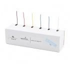
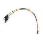
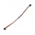
For those that want to take advantage of the Qwiic enabled devices, you'll want to grab a Qwiic cable.
If you aren't familiar with the MicroMod ecosystem, we recommend reading here for an overview. We recommend reading here for an overview if you decide to take advantage of the Qwiic connector.
 |
|
| MicroMod Ecosystem | Qwiic Connect System |
If you aren’t familiar with the following concepts, we also recommend checking out a few of these tutorials before continuing.
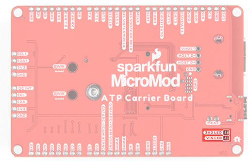
The MicroMod ATP Carrier Board includes a location for a MicroMod Processor Board. Here is where your chosen Processor Board will reside.
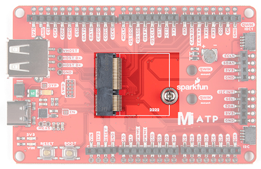
There are a variety of power-related nets broken out to female header pins and their corresponding through hole pads. The image below highlights those female headers and pads. The board can be powered from the VIN pin with a recommended voltage between 3.3V to 6.0V. It can also be powered with 5V from the USB C connector. The voltage is regulated down to 3.3V with the AP7361C voltage regulator to power your devices with up to 1A of current. If your voltage is clean, and regulated, you can also connect it directly to the 3.3V line.
The board has a built-in backup battery for Processor Boards with an RTC. Depending on the processor, it may not be connected
You have the option of connecting the board to a computer using the USB connectors. The USB Type C connector is used to power, program the processor board, or pass serial data to a serial terminal. If your processor board has dedicated pins broken out for USB host, there is an option for USB host through the female USB Type A connector. There is a Schottky diode on the USB host's 5V pin to prevent conflicting voltages from the USB host device and USB-C connector. If necessary, you can bypass the diode to power the USB host device by adding a wire between the VHOST pin and VIN pin.
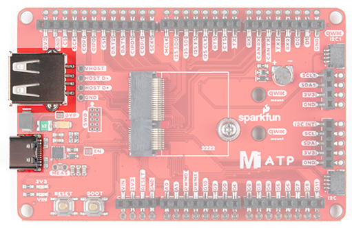
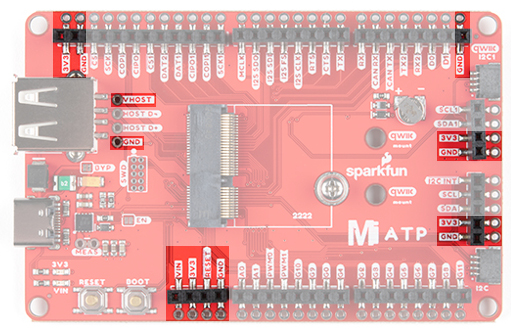
Remember our "All the Pins!" nickname? Well, we meant it. On the MicroMod ATP, we broke out all the major pins using the general MicroMod hardware pinout v1.0 from the M.2 connector to the female headers. We've also added a secondary rail of plated through-holes alongside them to give you the choice of either plug and play or soldering directly to the board. Your mileage may vary depending on the processor board that you are using.
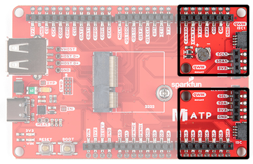
There are two locations on the board for your favorite Qwiic-enabled device. In addition to the Qwiic connectors, we also have pins that are broken out on the should you need to use jumper wires or solder wire direction to both boards. If you look closely at the port labeled as I2C, there is a dedicated I2C interrupt pin available.
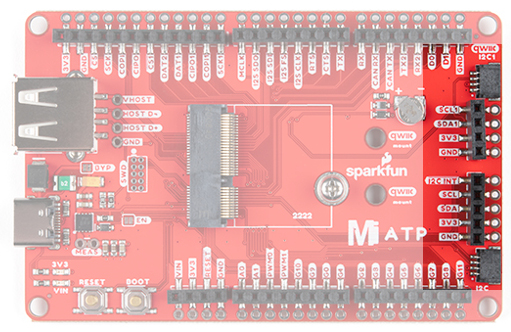
There are mounting holes to attach each standard 1.0"x1.0" Qwiic-enabled device.
The reset button will reset the processor. The boot button will put the processor into a special boot mode. Depending on the processor board, this boot pin may not be connected.
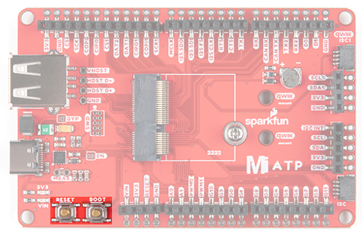
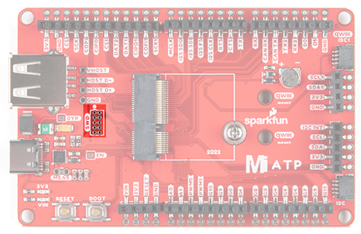
For advanced users, we broke out the SWD programming pins. Note that this is not populated so you will need a compatible header and compatible JTAG programmer to connect.
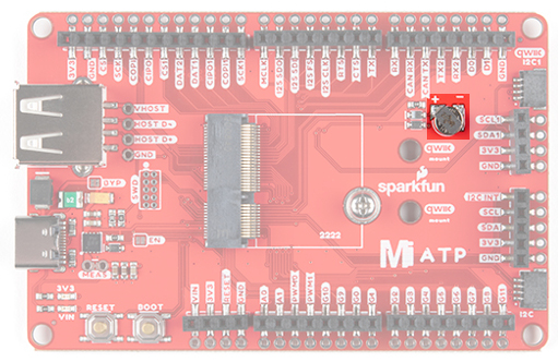
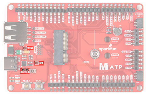
There are two LEDs on the board.
There are a few jumpers populated on the board:
 |
 |
| Jumpers on the Top Side | Jumpers on the Back Side |
Wondering what the pins are that are broken out on the ATP MicroMod ATP Carrier Board? Check out the table from the Getting Started with MicroMod for more information. Remember to check out the pins against your Processor Board to determine what pins are available.
| AUDIO | UART | GPIO/BUS | I2C | SDIO | SPI0 | Dedicated |
| Function | Bottom Pin |
Top Pin |
Function | ||||||
|---|---|---|---|---|---|---|---|---|---|
| (Not Connected) | 75 | GND | |||||||
| 3.3V | 74 | 73 | G5 / BUS5 | ||||||
| RTC_3V_BATT | 72 | 71 | G6 / BUS6 | ||||||
| SPI_CS1# | SDIO_DATA3 (I/O) | 70 | 69 | G7 / BUS7 | |||||
| SDIO_DATA2 (I/O) | 68 | 67 | G8 | ||||||
| SDIO_DATA1 (I/O) | 66 | 65 | G9 | ADC_D- | CAM_HSYNC | ||||
| SPI_CIPO1 | SDIO_DATA0 (I/O) | 64 | 63 | G10 | ADC_D+ | CAM_VSYNC | |||
| SPI COPI1 | SDIO_CMD (I/O) | 62 | 61 | SPI_CIPO (I) | |||||
| SPI SCK1 | SDIO_SCK (O) | 60 | 59 | SPI_COPI (O) | LED_DAT | ||||
| AUD_MCLK (O) | 58 | 57 | SPI_SCK (O) | LED_CLK | |||||
| CAM_MCLK | PCM_OUT | I2S_OUT | AUD_OUT | 56 | 55 | SPI_CS# | |||
| CAM_PCLK | PCM_IN | I2S_IN | AUD_IN | 54 | 53 | I2C_SCL1 (I/O) | |||
| PDM_DATA | PCM_SYNC | I2S_WS | AUD_LRCLK | 52 | 51 | I2C_SDA1 (I/O) | |||
| PDM_CLK | PCM_CLK | I2S_SCK | AUD_BCLK | 50 | 49 | BATT_VIN / 3 (I - ADC) (0 to 3.3V) | |||
| G4 / BUS4 | 48 | 47 | PWM1 | ||||||
| G3 / BUS3 | 46 | 45 | GND | ||||||
| G2 / BUS2 | 44 | 43 | CAN_TX | ||||||
| G1 / BUS1 | 42 | 41 | CAN_RX | ||||||
| G0 / BUS0 | 40 | 39 | GND | ||||||
| A1 | 38 | 37 | USBHOST_D- | ||||||
| GND | 36 | 35 | USBHOST_D+ | ||||||
| A0 | 34 | 33 | GND | ||||||
| PWM0 | 32 | 31 | Module Key | ||||||
| Module Key | 30 | 29 | Module Key | ||||||
| Module Key | 28 | 27 | Module Key | ||||||
| Module Key | 26 | 25 | Module Key | ||||||
| Module Key | 24 | 23 | SWDIO | ||||||
| UART_TX2 (O) | 22 | 21 | SWDCK | ||||||
| UART_RX2 (I) | 20 | 19 | UART_RX1 (I) | ||||||
| CAM_TRIG | D1 | 18 | 17 | UART_TX1 (0) | |||||
| I2C_INT# | 16 | 15 | UART_CTS1 (I) | ||||||
| I2C_SCL (I/0) | 14 | 13 | UART_RTS1 (O) | ||||||
| I2C_SDA (I/0) | 12 | 11 | BOOT (I - Open Drain) | ||||||
| D0 | 10 | 9 | USB_VIN | ||||||
| SWO | G11 | 8 | 7 | GND | |||||
| RESET# (I - Open Drain) | 6 | 5 | USB_D- | ||||||
| 3.3V_EN | 4 | 3 | USB_D+ | ||||||
| 3.3V | 2 | 1 | GND | ||||||
| Signal Group | Signal | I/O | Description | Voltage | Power | 3.3V | I | 3.3V Source | 3.3V |
|---|---|---|---|---|
| GND | Return current path | 0V | ||
| USB_VIN | I | USB VIN compliant to USB 2.0 specification. Connect to pins on processor board that require 5V for USB functionality | 4.8-5.2V | |
| RTC_3V_BATT | I | 3V provided by external coin cell or mini battery. Max draw=100μA. Connect to pins maintaining an RTC during power loss. Can be left NC. | 3V | |
| 3.3V_EN | O | Controls the carrier board's main voltage regulator. Voltage above 1V will enable 3.3V power path. | 3.3V | |
| BATT_VIN/3 | I | Carrier board raw voltage over 3. 1/3 resistor divider is implemented on carrier board. Amplify the analog signal as needed for full 0-3.3V range | 3.3V | |
| Reset | Reset | I | Input to processor. Open drain with pullup on processor board. Pulling low resets processor. | 3.3V |
| Boot | I | Input to processor. Open drain with pullup on processor board. Pulling low puts processor into special boot mode. Can be left NC. | 3.3V | |
| USB | USB_D± | I/O | USB Data ±. Differential serial data interface compliant to USB 2.0 specification. If UART is required for programming, USB± must be routed to a USB-to-serial conversion IC on the processor board. | |
| USB Host | USBHOST_D± | I/O | For processors that support USB Host Mode. USB Data±. Differential serial data interface compliant to USB 2.0 specification. Can be left NC. | |
| CAN | CAN_RX | I | CAN Bus receive data. | 3.3V |
| CAN_TX | O | CAN Bus transmit data. | 3.3V | |
| UART | UART_RX1 | I | UART receive data. | 3.3V |
| UART_TX1 | O | UART transmit data. | 3.3V | |
| UART_RTS1 | O | UART ready to send. | 3.3V | |
| UART_CTS1 | I | UART clear to send. | 3.3V | |
| UART_RX2 | I | 2nd UART receive data. | 3.3V | |
| UART_TX2 | O | 2nd UART transmit data. | 3.3V | |
| I2C | I2C_SCL | I/O | I2C clock. Open drain with pullup on carrier board. | 3.3V |
| I2C_SDA | I/O | I2C data. Open drain with pullup on carrier board | 3.3V | |
| I2C_INT# | I | Interrupt notification from carrier board to processor. Open drain with pullup on carrier board. Active LOW | 3.3V | |
| I2C_SCL1 | I/O | 2nd I2C clock. Open drain with pullup on carrier board. | 3.3V | |
| I2C_SDA1 | I/O | 2nd I2C data. Open drain with pullup on carrier board. | 3.3V | |
| SPI | SPI_COPI | O | SPI Controller Output/Peripheral Input. | 3.3V |
| SPI_CIPO | I | SPI Controller Input/Peripheral Output. | 3.3V | |
| SPI_SCK | O | SPI Clock. | 3.3V | |
| SPI_CS# | O | SPI Chip Select. Active LOW. Can be routed to GPIO if hardware CS is unused. | 3.3V | |
| SPI/SDIO | SPI_SCK1/SDIO_CLK | O | 2nd SPI Clock. Secondary use is SDIO Clock. | 3.3V |
| SPI_COPI1/SDIO_CMD | I/O | 2nd SPI Controller Output/Peripheral Input. Secondary use is SDIO command interface. | 3.3V | |
| SPI_CIPO1/SDIO_DATA0 | I/O | 2nd SPI Peripheral Input/Controller Output. Secondary use is SDIO data exchange bit 0. | 3.3V | |
| SDIO_DATA1 | I/O | SDIO data exchange bit 1. | 3.3V | |
| SDIO_DATA2 | I/O | SDIO data exchange bit 2. | 3.3V | |
| SPI_CS1/SDIO_DATA3 | I/O | 2nd SPI Chip Select. Secondary use is SDIO data exchange bit 3. | 3.3V | |
| Audio | AUD_MCLK | O | Audio master clock. | 3.3V |
| AUD_OUT/PCM_OUT/I2S_OUT/CAM_MCLK | O | Audio data output. PCM synchronous data output. I2S serial data out. Camera master clock. | 3.3V | |
| AUD_IN/PCM_IN/I2S_IN/CAM_PCLK | I | Audio data input. PCM syncrhonous data input. I2S serial data in. Camera periphperal clock. | 3.3V | |
| AUD_LRCLK/PCM_SYNC/I2S_WS/PDM_DATA | I/O | Audio left/right clock. PCM syncrhonous data SYNC. I2S word select. PDM data. | 3.3V | |
| AUD_BCLK/PCM_CLK/I2S_CLK/PDM_CLK | O | Audio bit clock. PCM clock. I2S continuous serial clock. PDM clock. | 3.3V | |
| SWD | SWDIO | I/O | Serial Wire Debug I/O. Connect if processor board supports SWD. Can be left NC. | 3.3V |
| SWDCK | I | Serial Wire Debug clock. Connect if processor board supports SWD. Can be left NC. | 3.3V | |
| ADC | A0 | I | Analog to digital converter 0. Amplify the analog signal as needed to enable full 0-3.3V range. | 3.3V |
| A1 | I | Analog to digital converter 1. Amplify the analog signal as needed to enable full 0-3.3V range. | 3.3V | |
| PWM | PWM0 | O | Pulse width modulated output 0. | 3.3V |
| PWM1 | O | Pulse width modulated output 1. | 3.3V | |
| Digital | D0 | I/O | General digital input/output pin. | 3.3V |
| D1/CAM_TRIG | I/O | General digital input/output pin. Camera trigger. | 3.3V | |
| General/Bus | G0/BUS0 | I/O | General purpose pins. Any unused processor pins should be assigned to Gx with ADC + PWM capable pins given priority (0, 1, 2, etc.) positions. The intent is to guarantee PWM, ADC and Digital Pin functionality on respective ADC/PWM/Digital pins. Gx pins do not guarantee ADC/PWM function. Alternative use is pins can support a fast read/write 8-bit or 4-bit wide bus. | 3.3V |
| G1/BUS1 | I/O | 3.3V | ||
| G2/BUS2 | I/O | 3.3V | ||
| G3/BUS3 | I/O | 3.3V | ||
| G4/BUS4 | I/O | 3.3V | ||
| G5/BUS5 | I/O | 3.3V | ||
| G6/BUS6 | I/O | 3.3V | ||
| G7/BUS7 | I/O | 3.3V | ||
| G8 | I/O | General purpose pin | 3.3V | |
| G9/ADC_D-/CAM_HSYNC | I/O | Differential ADC input if available. Camera horizontal sync. | 3.3V | |
| G10/ADC_D+/CAM_VSYNC | I/O | Differential ADC input if available. Camera vertical sync. | 3.3V | |
| G11/SWO | I/O | General purpose pin. Serial Wire Output | 3.3V |
The board is 3.30"x2.20". There are 4x mounting holes on each corner of the board. There are 2x additional mounting holes by the SparkFun logo for Qwiic-enabled devices.

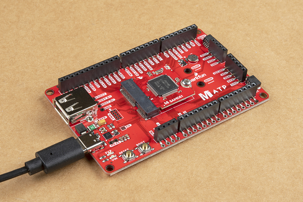
If you have not already, make sure to check out the Getting Started with MicroMod: Hardware Hookup for information on inserting your Processor Board to your Carrier Board.
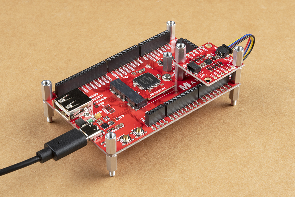
At a minimum, your setup should look like the image below. In this case, we had the MicroMod SAMD51 Processor Board secured in the M.2 connector. To program and power the microcontroller, we inserted the USB-C cable.
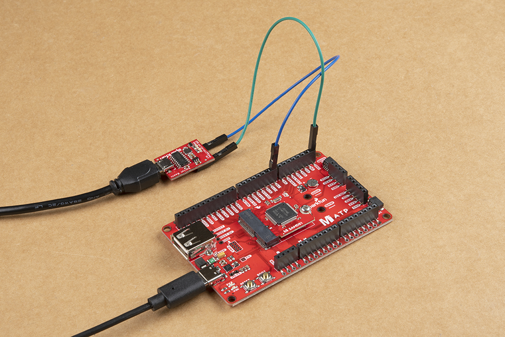
Depending on your setup you may need hardware (jumper wire, cables, header pins, breadboard, etc.) to connect to the board. In this case, we used jumper wire to connect to another board.
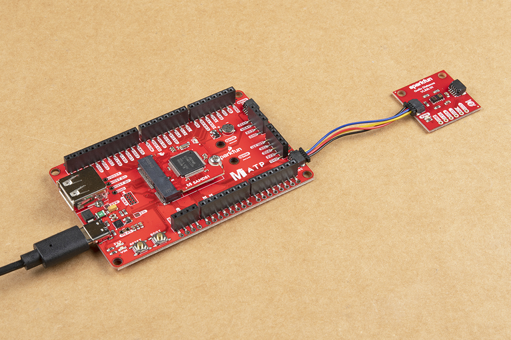
To Qwiic-ly connect I2C devices, simply insert a Qwiic cable between the MicroMod ATP's Qwiic port and your Qwiic device.
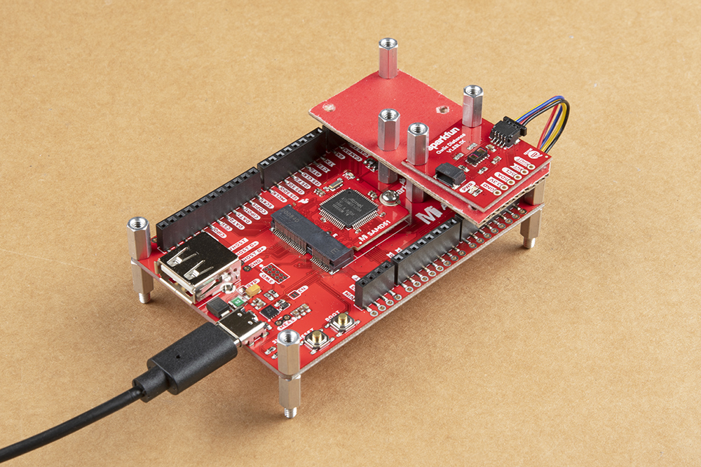
To secure the boards together, you could add standoffs and screws to mount a Qwiic-enabled device that have the standard 1.0"x1.0" sized board. Keep in mind that this will block a few of the header pins below so make sure to plan accordingly.
Depending on the location of the mounting holes, you may need to make an adapter to hold the Qwiic-enabled device securely. Below is an example with mounting holes on the same side instead of diagonal. A piece of cardboard was cut out as shown in the image below. Depending on your personal preference, you could also laser cut, CNC, or 3D printer to make a more sturdy panel for those that need a stronger material.
There are quite a lot of peripherals broken out on the MicroMod ATP Carrier Board. Depending on the design of the Processor Board, not all of the pins may be broken out. For simplicity, we will upload a blink sketch to get started.
Now that you have a Processor Board secure in the Carrier Board, let's upload a simple blink sketch to the board. Copy and paste the following code in the Arduino IDE. Head to Tools > Board to select the correct board definition (in this case, SparkFun MicroMod SAMD51. Select the correct COM port that the board enumerated to. Hit upload.
language:c
/*
  Blink
  Turns on an LED on for one second, then off for one second, repeatedly.

  This example code is in the public domain.
*/

// Pin 13 has an LED connected on most Arduino boards.
// give it a name
// uncomment the following lines if the macro is not defined for your architecture
//#define LED_BUILTIN 13 //Artemis, SAMD51
//#define LED_BUILTIN 5 //ESP32

// the setup routine runs once when you press reset:
void setup() {
  // initialize the digital pin using the built-in macro as an output.
  pinMode(LED_BUILTIN, OUTPUT);
}

// the loop routine runs over and over again forever:
void loop() {
  digitalWrite(LED_BUILTIN, HIGH);   // turn the LED on (HIGH is the voltage level)
  delay(1000);               // wait for a second
  digitalWrite(LED_BUILTIN, LOW);    // turn the LED off by making the voltage LOW
  delay(1000);               // wait for a second
}
After uploading, you should see the Processor Board's LED blink. If not, make sure that to define the pin and check your connections.
What's next? Try building a circuit using the design files and associated tutorial for your Processor Board more information. Keep in mind that while each Processor Board uses the same MicroMod interface pinout, each board may have different specifications, software support, and peripherals available for the architecture.
Now that you've successfully got your MicroMod ATP Carrier Board up and running with your Processor Board, it's time to incorporate it into your own project! For more information, check out the resources below:
Need some inspiration for your next project? Check out some of these related tutorials with MicroMod:
Or check out some of these related blog posts for more ideas!
learn.sparkfun.com | CC BY-SA 3.0 | SparkFun Electronics | Niwot, Colorado