Designing with the SparkFun Artemis
 Nate, Ell C
Hardware Overview
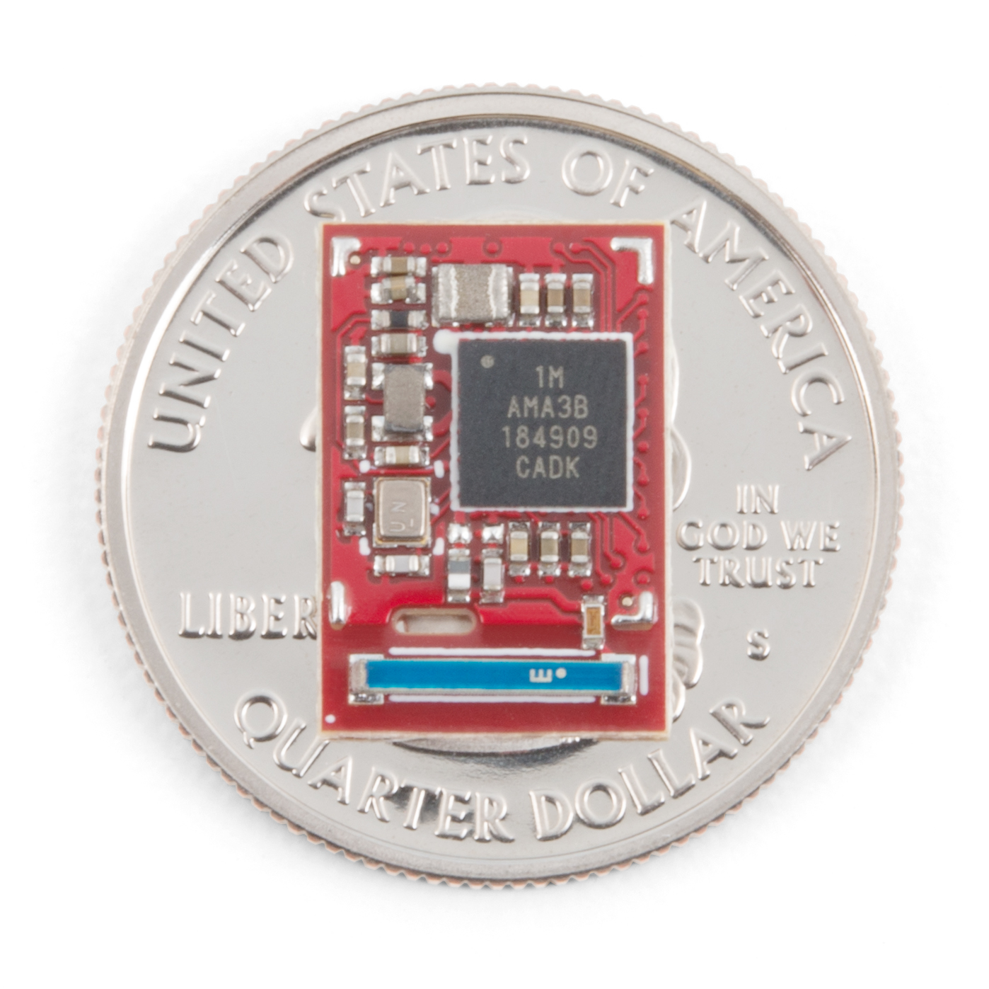
This section covers the technical details of the Artemis including the footprint and electrical characteristics. If you’ve already got a dev board with the Artemis module mounted, you can skip this section and head to Unique Features. That said, when was the last time you got to actually see inside one of these modules?
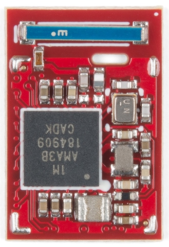
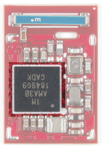
Apollo3
The core of the Artemis module is the Apollo3 by Ambiq. This is an ARM Cortex-M4F (F indicates hardware floating point operations) with 1M of flash and 384k of RAM. The datasheet is available here.
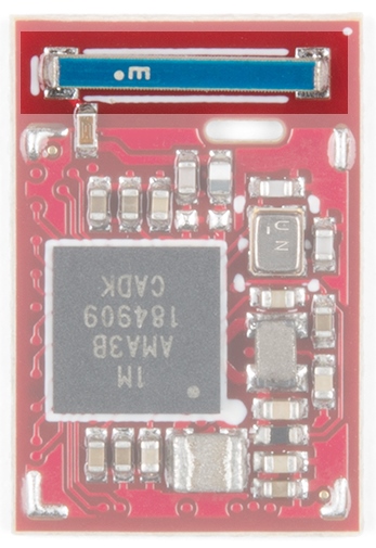
BLE Antenna
The Apollo3 has a built-in Bluetooth 5.0 radio and the module has a built in 2.4GHz antenna with 2dBi of gain.
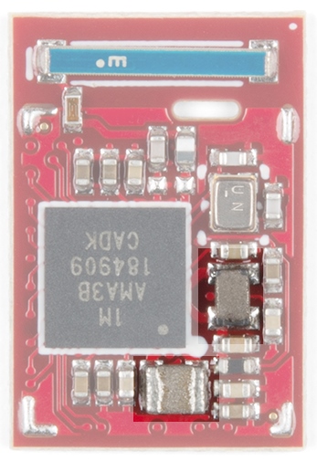
Onboard DC Buck
The Apollo3 can operate from 3.6 to 1.8V. To allow for such a large window the Apollo3 has two built in DC buck circuits that regulate the input VCC down to the core voltage with >80% efficiency. The Artemis module includes two inductors to allow for minimum power consumption.
Dimensions
The module measures 15.5 x 10.5 x 2.3mm and weighs 0.6 grams.
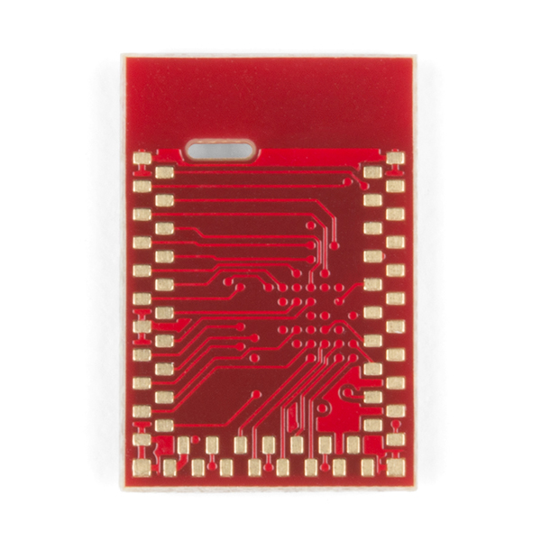
Recommended Footprint
The recommended PCB layout for the module is shown here:
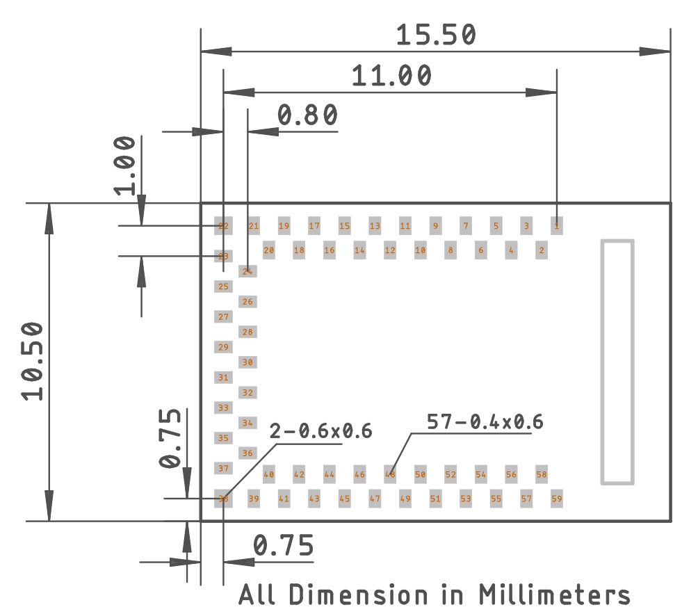
Be sure to checkout the Artemis Integration Guide for specific dimensions and considerations. If you design with EAGLE PCB simply clone one of our open source hardware designs that utilize the Artemis (RedBoard Artemis, RedBoard Artemis Nano, and RedBoard Artemis ATP) and begin laying out your board!
The Apollo3 is a powerful IC but its 0.5mm BGA package requires a 4 layer PCB with buried and epoxy-filled vias. This makes the PCBs expensive and difficult to produce. We designed Artemis to rid you of these concerns.
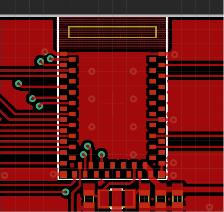
Laying out a PCB with Artemis can be done on a 2-layer PCB with 8mil trace/space. Routing under the module is allowed. Keep all ground pours away from the antenna area. If mechanical exposure allows for it the antenna can be extended over the edge of the PCB for increased reception.