Designing PCBs: Advanced SMD
 Nate
Nate 
Laying Out the PCB
Now let’s click on the ‘Board’ button and start PCB layout!
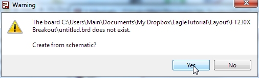
Yes please create from schematic.
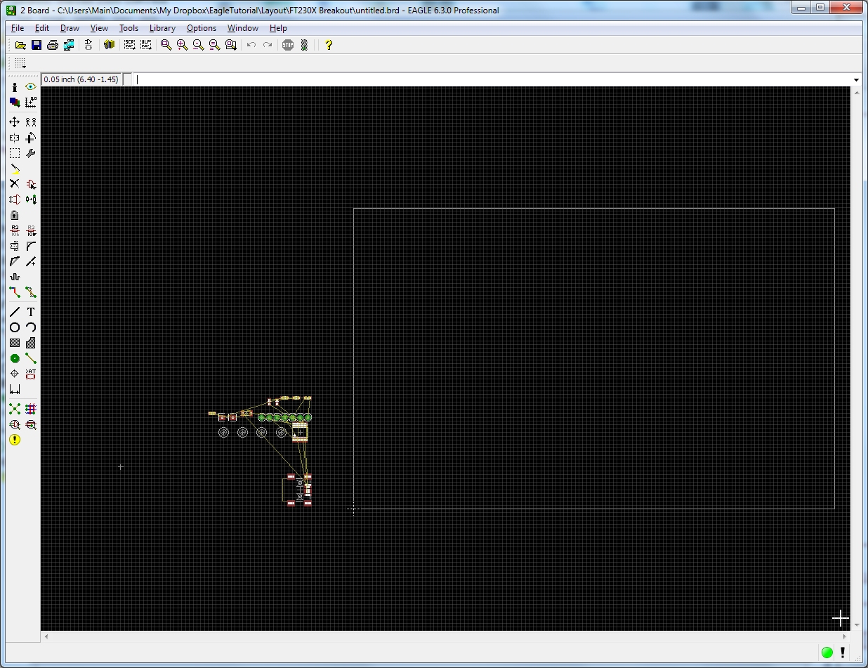
Whoa! Neat! Use the mouse wheel to zoom in and out. Click the mouse wheel and move the mouse to navigate around an area.
Now press F7 to go into ‘move’ mode. Begin to move the parts to the lower corner of the PCB.
As you’re moving stuff around, right click to rotate a part.
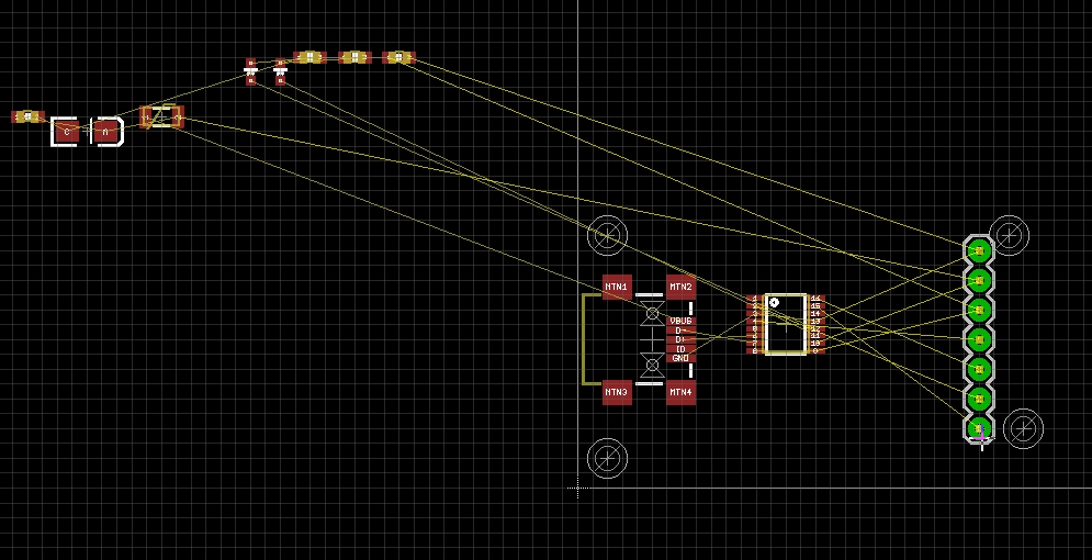
You’ll see the rats nest of airwires update as you go. Be looking to rotate or position a component to try to minimize the overlap of wires. You won’t get it all straightened out but this is the time to be thinking about it. Decent placement at this stage will make routing much easier later on. Regularly press F8 to update the rats nest.
We are getting there.
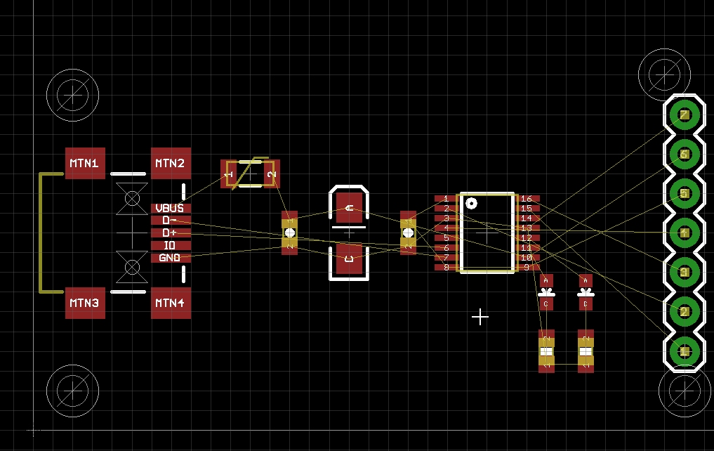
We now need to reduce the board shape to fit our rough arrangement of parts. You should see a thin white wire that makes a big square. This wire is on the dimension layer and represents your outer board shape. Press F7 then click on the white wire and move the sides of the board inward, making a tight box around your components.
Note: The USB connector can hang slightly over the edge.
Also, see the board outline near the cursor is not ‘on grid’? Press F7 to go into ‘move’ mode. Then hold Ctrl while clicking on the corner of the dimension line.
The wire or component (whatever you’re near) will jump onto the grid. This is a valuable trick to get stuff back on grid. Repeat with the upper right corner and lower left corner.
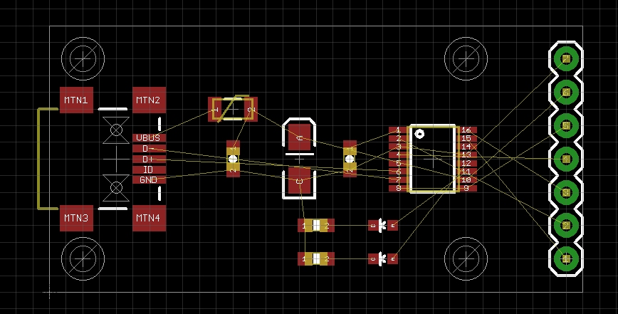
Ok - we’ve got everything packed in together pretty well. Take note of a couple things:
- Draw a horizontal line across the middle of the board. You'll notice I've located a lot of the components along the midline. This helps with aesthetics more than anything but also helps with some routing.
- Do not attempt to pack everything in right next to each other. You will eventually be soldering these parts to the board and will need some room to get the iron and solder wick in there.
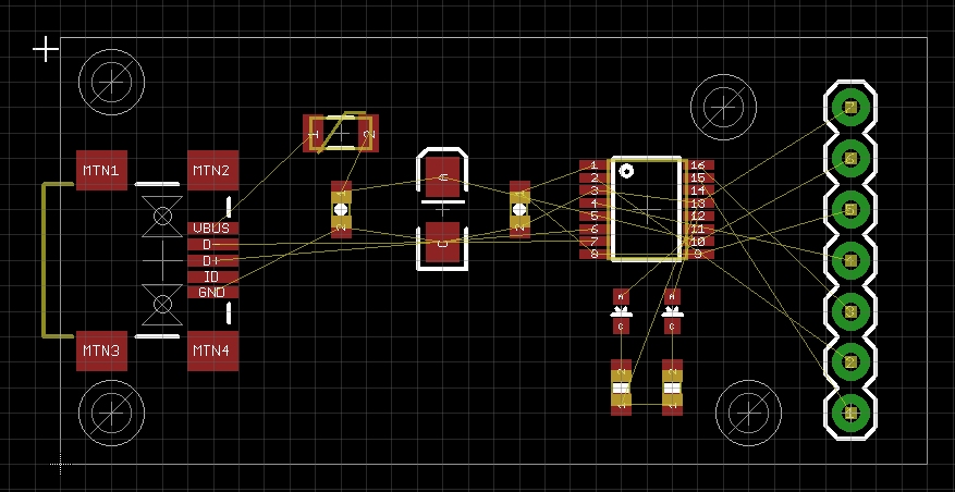
Let’s take a moment to turn on ALL the layers to see if there are any problems. Click on display, then the ‘All’ button, then Ok.
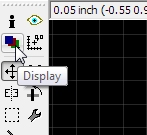
We’ve got a couple problems. There’s some text we didn’t even know about (the creative commons license! Yay!). And you also see red rings around the stand-offs. These rings are on the ‘top keepout’ layer. They are there to show the radius of the head of a standard screw. If we tried to put a screw into the breakout board it would hit the USB connector! Better spread things out.
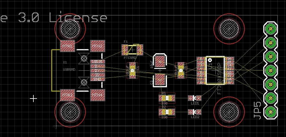
Use the scroll wheel to zoom out. Hit F7 to grab and move the license below your board.
Remember to use the Alt+F7 group command to group stuff together, then press F7 to go into 'move' mode, then Ctrl+right click to move the group. I used this trick to grab two standoff holes and the frame at the same time and made the board wider. Then grab more bits and bumped them up a few clicks.
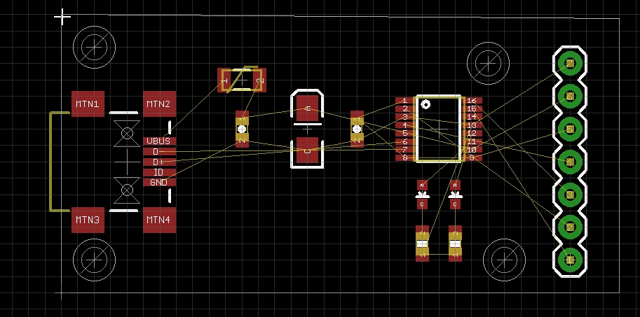
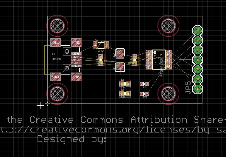
Now press F11 to return all the layers to their original / default viewing state. This allows us to concentrate on layout. Let’s start routing! We’re going to route this board by hand to show more advanced routing techniques. You are welcome to use the auto-router if you please.
At SparkFun we route everything by hand. Yes, everything. This is a change from my views a few years ago. We used to auto-route everything. The boards worked, but they looked awful. We like to think we should be pushing for a board that not only works but also looks good. Did I mention routing a board is like solving a puzzle? And I love puzzles!
Here is a quick breakdown of the key commands we’ll be using:
- Press F9 to lay a trace
- Alt F9 to rip up one
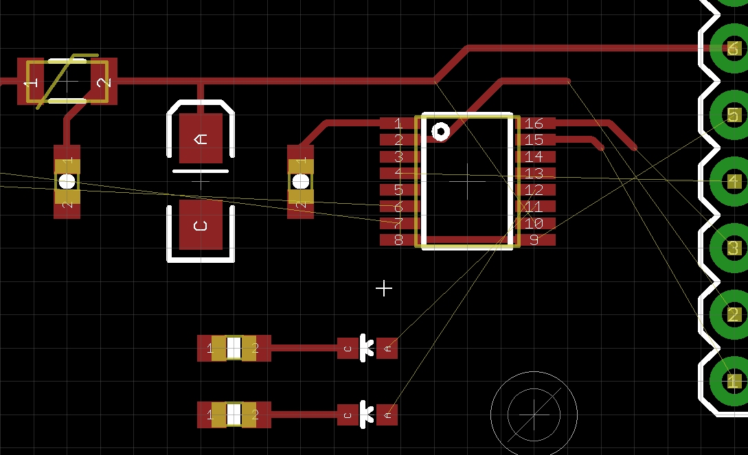
Click on the middle of pad VBUS. Drag out the wire to a grid intersection (it’ll snap to it). Click again to anchor the trace, then click again to stop routing that trace.
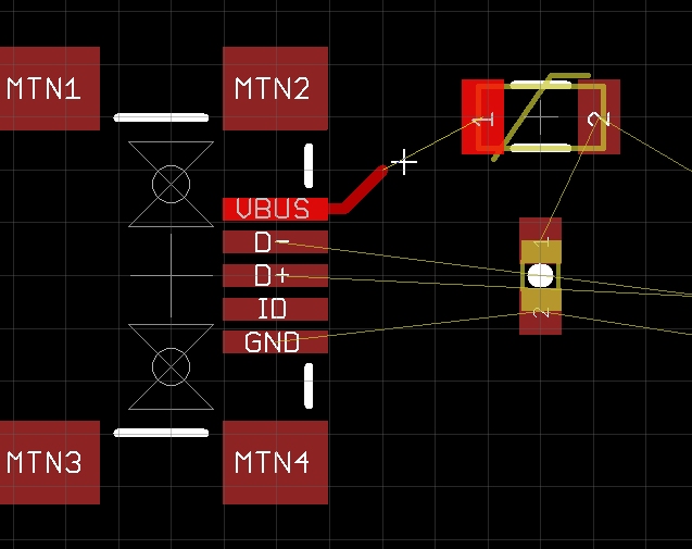
Now start routing from the PTC. Click on the ‘1’ pad. Drag trace out to intersection and down to other trace. You may hear a pleasant ‘ding’ letting you know the trace is completed.
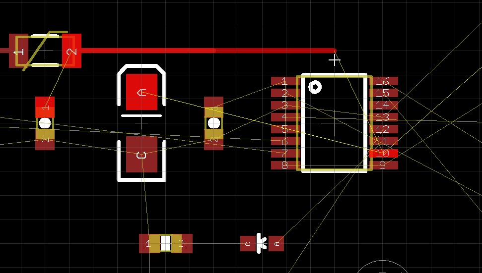
Continue the route after the PTC. Note that it goes down to the right side of the FT230X. I’m worried about boxing out other traces so I’ll just leave a stub of the trace here by double clicking.
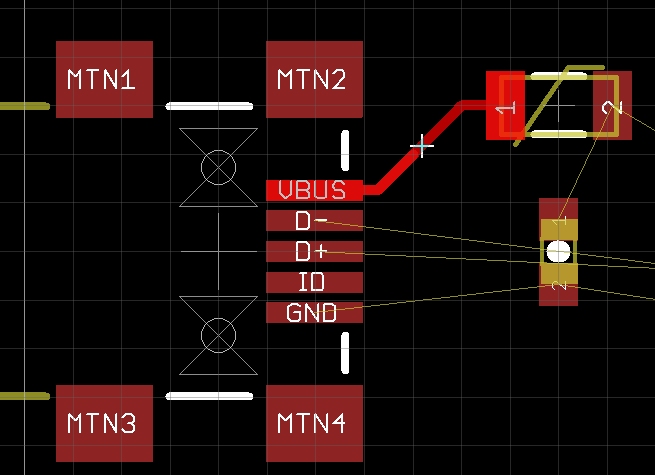
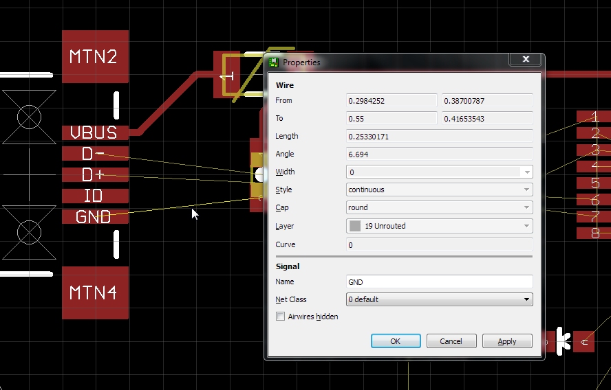
The GND airwires are distracting me. Click on the ‘i’ and then a GND wire. See the box at the bottom that says ‘Airwires Hidden’? Check that box and click ok. This will make all the ground airwires disappear. We’ll get the GND wires with a polygon pour later on.
Start attacking the easiest routes. Leave stubs where you see cross-over problems. See how far you can get without using a via. We'll talk about those next!