Designing PCBs: Advanced SMD
 Nate
Nate 
Gerber Generation
This layout is done! Now let’s generate some gerbers and get this board made! Hit F11 to turn on all the standard layers then click on CAM. If you don’t have the SparkFun CAM file, grab it here and put it in your Eagle\cam directory or, what I recommend, is to put this CAM file on a Dropbox folder that way you use the same CAM file between different version of Eagle and different computers.
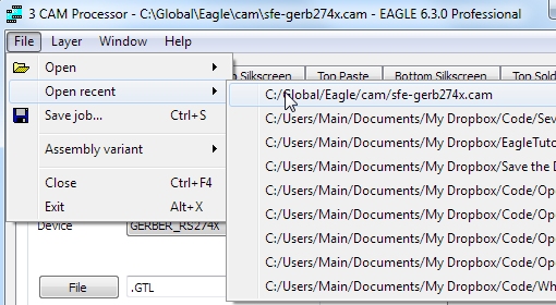
From within the CAM window, click on File->Open and located the sfe-gerb274X file. Once you’ve got the sfe-gerb274x.cam open, click ‘Process Job’. A few windows will pop up then close. Now go look in the folder that contains FT230X-Breakout:
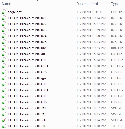
The *.brd and *.sch files are the main Eagle files. If you want to post or share your design with a friend online, these are the two files you need to zip and send them.
All the files ending in *.b#1, .b#2, .s#1, .s#5, etc are backups. Every time you save the schematic or board Eagle will create a new b#_ file and save the previous brd file to it. This is handy if you need to revert back to a version you were working on.
The *.gpi (general photoplotter information) and *.dri (drill information) are generally not needed by the PCB fabrication house.
The main gerber files you need to grab:
- *.GBL - Bottom copper layer
- *.GBO - Bottom overlay (silkscreen)
- *.GBS - Bottom soldermask
- *.GTL - Top copper layer
- *.GTO - Top overlay (silkscreen)
- *.GTS - Top soldermask
- *.TXT - Drill file (coordinate information)
Note there is no dimension file in this list. The dimension layer gets exported to the top copper layer using our CAM file. Your fab house can probably work with this but may want something different.
You will probably see a *.GTP file. This is the top paste layer. At SparkFun, we use this layer to have a paste stencil cut. Stencil solder paste and doing SMD reflow is super helpful if you are running more than 3 or 4 boards. You can absolutely stencil, build, and reflow PCBs without big, expensive equipment! And you can even cut stencils at home.
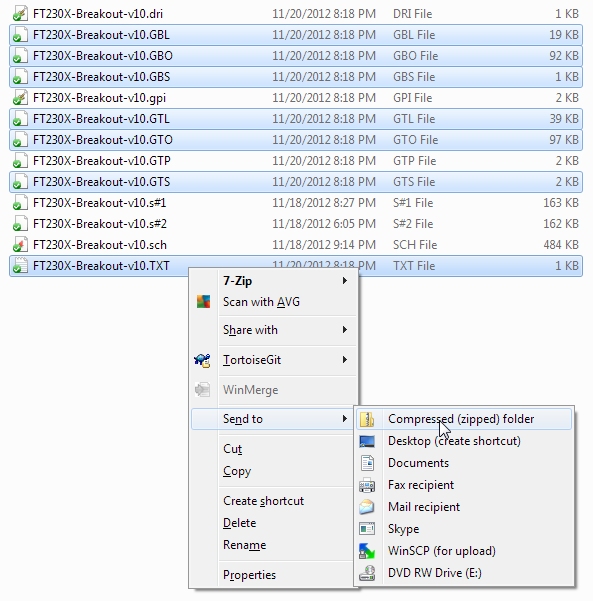
Select the gerber files and drill file, 7 in all. Do this by clicking on the first file, then hold Ctrl, then click on each additional file. Right click and under Windows 7 you can Send To a zip file. Zip together however you are most accustom.
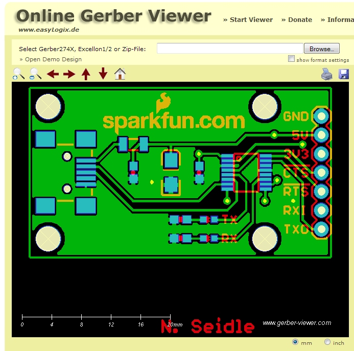
I just recently found www.gerber-viewer.com. They have a pretty good interface for inspecting your gerber files. I highly recommend you use a gerber viewer separate from Eagle before you send them off.
With your gerber files in hand, email your favorite PCB fab house. Most fab houses are setup to do:
- Silkscreen one side
- Green soldermask
- White silkscreen
- 1.6mm thick FR4 PCB
Almost all PCBs have these specs but doing fancier PCBs is getting cheaper and cheaper. All our products are made with red soldermask and have silkscreen on both sides. Our LilyPad line is 0.8mm thick with purple soldermask. If you’re just doing protos, stick with the standard setup. If you’re doing a production run, get creative!
Now go play some Portal 2 while you wait for your PCBs to come back. It can take anywhere from a few days to a few weeks to get PCBs manufactured.