Designing PCBs: Advanced SMD
Design Rule Check
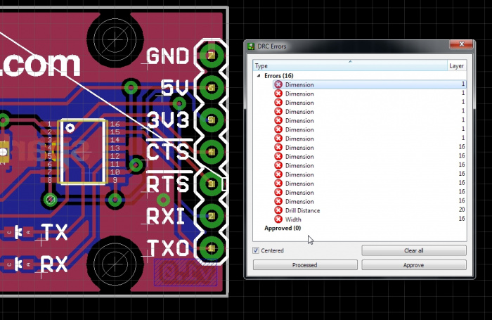
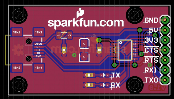
Time to run DRC on the board to make sure we've not made any electrical or mechnical mistakes. Let’s turn off the extra layers by pressing F11 and click on the DRC button, then ‘Check’.
Hmm... We’ve got some errors. This dimension error is because the annular ring of the connector is too close to the edge of the board. Remember when we increased the width of the board outline? This is being raised because of that. The risk here is that when the board is milled out it may nick the annular ring of this connector. SparkFun has a general policy that this is ok and this type of error, on a 0.01” connector can be dismissed. In the rare event that the ring is nicked, the connection and therefore the signal will survive. Click on ‘Approved’ through all the dimension errors.
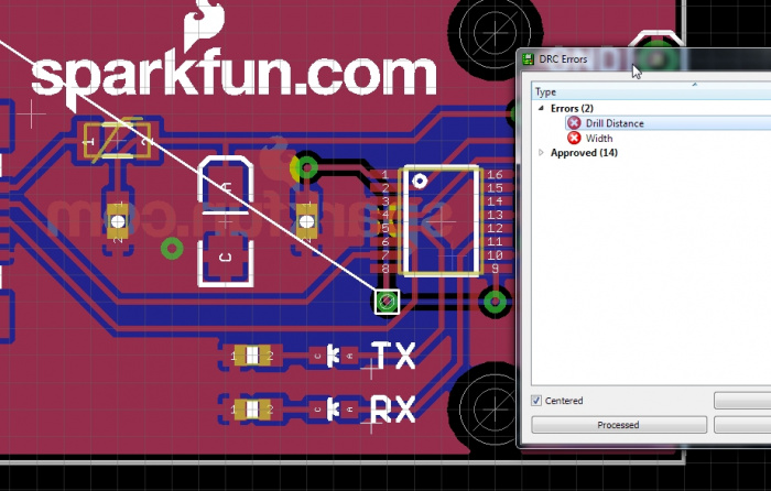
This is a valid error! Looks like I accidentally created two vias, right on top of one another when I was routing that really small airwire. To fix this, let’s alt+F9 rip up and click on that via to see if we can remove one.
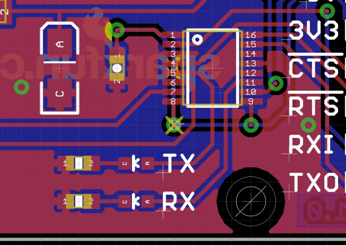
We’ve removed the via but Eagle is trying to tell us (with a big X) that something is still wrong. Hitting F8 ratsnest refresh doesn’t help, so I’m going to rip up those traces and re-route.
I ripped up those traces, then rerouted. I then re-ran DRC and Eagle is now happy. Error cleared.
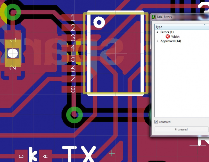
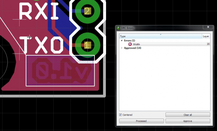
This is Eagle trying to tell us the trace width of this text is too thin. Normally fab houses don’t want traces thinner than 8mil (0.008”). This text violates that. Obviously, we and the fab house don’t care if these traces are broken because 'v1.0' is for informational purposes, not for signals. But the real way to correct this is to increase the text ratio so that the traces get bigger than 8mil. Hit the ‘i’ button, click on the text and increase the ‘ratio’ to 20%. Re-run the DRC and the error should clear.
Ok. We’re close to the finish line. Hit F8 and make sure there are no remaining airwires. Run DRC one last time to make sure there are no DRC errors.
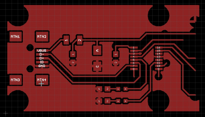
I often turn off everything but the top layer and look at the trace routing. Are there any traces that do anything really silly? Then I do the same for the bottom layer.
