Designing PCBs: Advanced SMD
 Nate
Nate 
Adding Labels
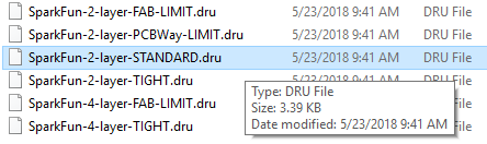
The default DRC rules with Eagle are a little too conservative in some areas, and very bad in others. Let’s load the SparkFun 2 layer standard dru file located here. For this board, we will use Click on the DRC button, then Load.
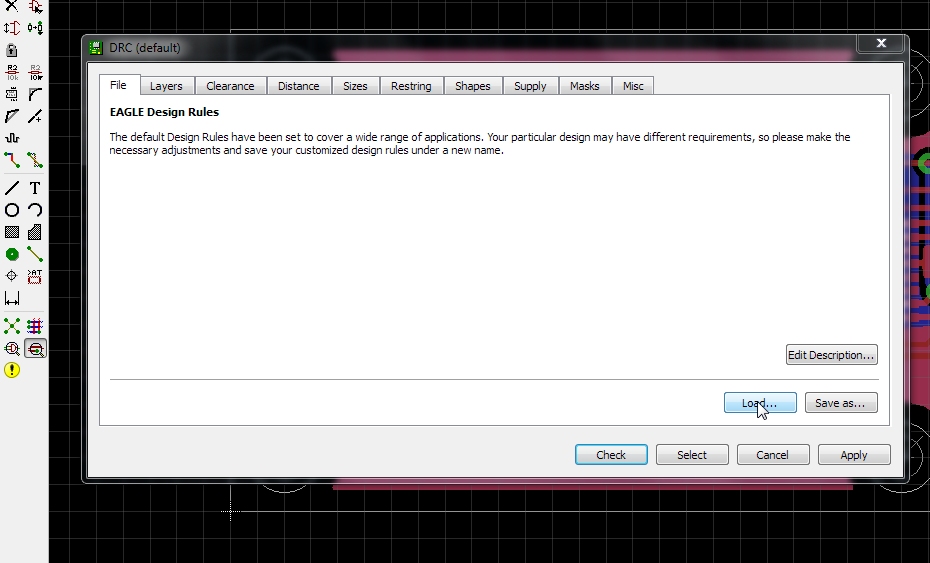
Double click the SparkFun.dru file then click ‘Select’ in the main DRC window. It should disappear.
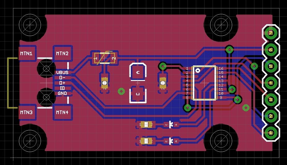
What? It looks the same. But wait! Hit F8 to do a ratsnest refresh. That looks a little better! The SparkFun DRU file reduces the amount of space between the copper layers and the dimension layer (the border of your board) from 40mil to 10mil.
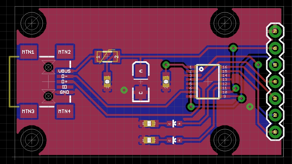
All these vias should work but they are pretty sloppy. The SparkFun design rules file increases the size of the annular rings around your vias. This gives the PCB fab houses a bigger ring to drill through the middle of, thus decreasing the chances the your board will be fabricated with errors.
Now let’s increase the width of the board outline from 0” to 0.008”. We do this so that we give the DRC (design rule checker) the chance to tell us if anything is too near the board edge. When the PCB fab house is routing boards apart, they use a very accurate milling machine, but let’s assume they’re not perfect. We use the width of the board outline to give us that level of extra safety.
To change the width of the board edge click on the wrench, then width, then ‘...’. Enter ‘0.008’ then click on the board edge. It will probably highlight the polygon pours. To get around this, right click and the next thing in the stack will highlight - it will probably be the other polygon pour so right click again. Finally the white line that makes up the board outline should be highlighted. Good - now left click to apply the width change. Now do that to the other three sides.
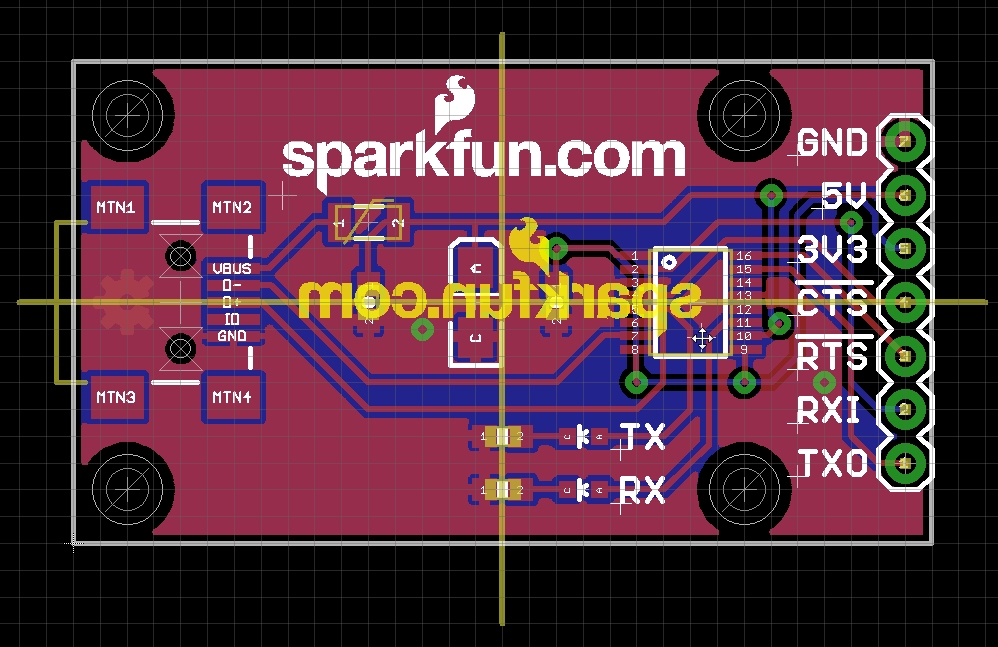
Now it’s time to label everything! Click the ‘Text’ button. A window will pop up, enter ‘TX’.
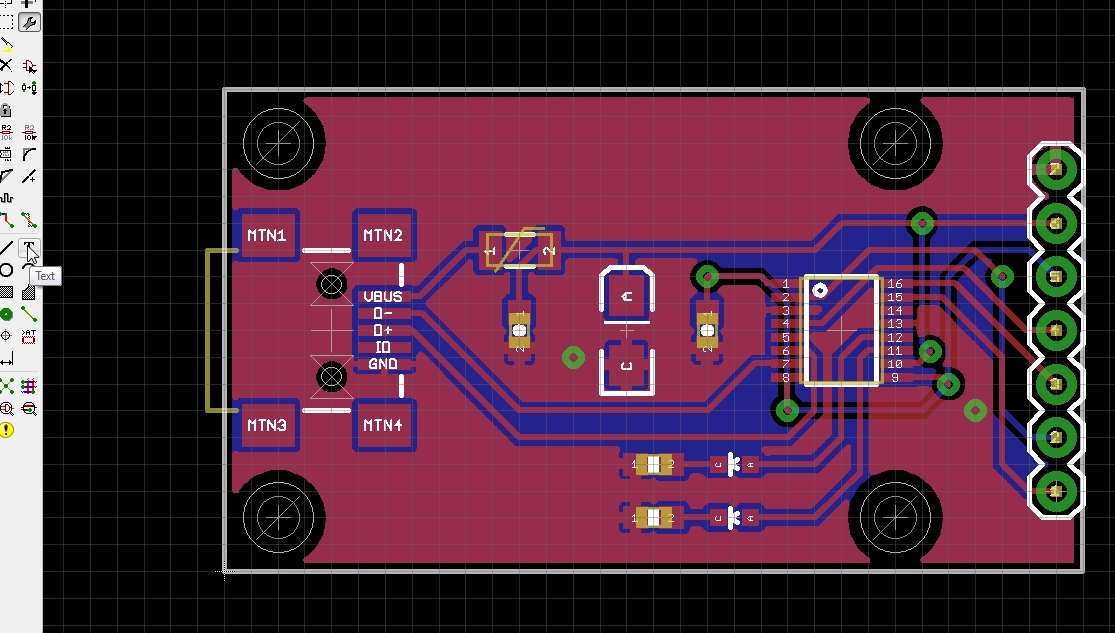
There will then be text on the bottom layer. No good. Click the middle mouse wheel and select ‘tPlace’. Anything on tPlace will be printed as silk. Hold the alt button and arrange the TX label next to the TX LED.
Pressing escape will bring you back to the text input window. Type 'RX' and add the label next to the other LED.
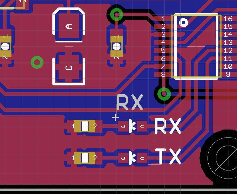
See how the X of TX and RX is bisected? I like centering text. I threw these labels down but I don’t actually know which LED is which. Let’s consult the FT230X datasheet:
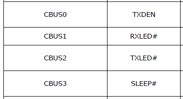
Ok, CBUS1 is RX LED, CBUS2 is TX LED. Let’s go look at our schematic:
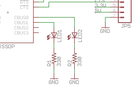
Oh no! I wired it wrong. Let’s delete those two wires (press F3 then click on the wire to remove), group the LED/Resistor/GND (alt+F7 then select, then F7), move them down (ctrl + right click), and add wires back (F9).
Let’s also label the nets so we will know on our layout which is which. Alt+F9 then click on a wire to add a label. Click again to anchor the label to the wire. F4 to rename the wire to RXLED (on CBUS1 pin). Repeat for CBUS2 wire label.
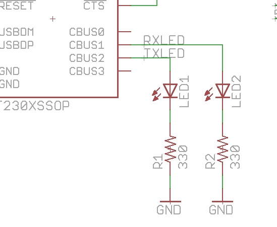
Ok fixed. Let’s go back to our layout.
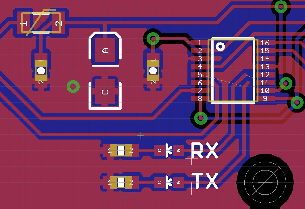
We’ve got some crossed wires. Rip up the traces that were there, swap the LED placement with the alt-F7 group command then re-route.
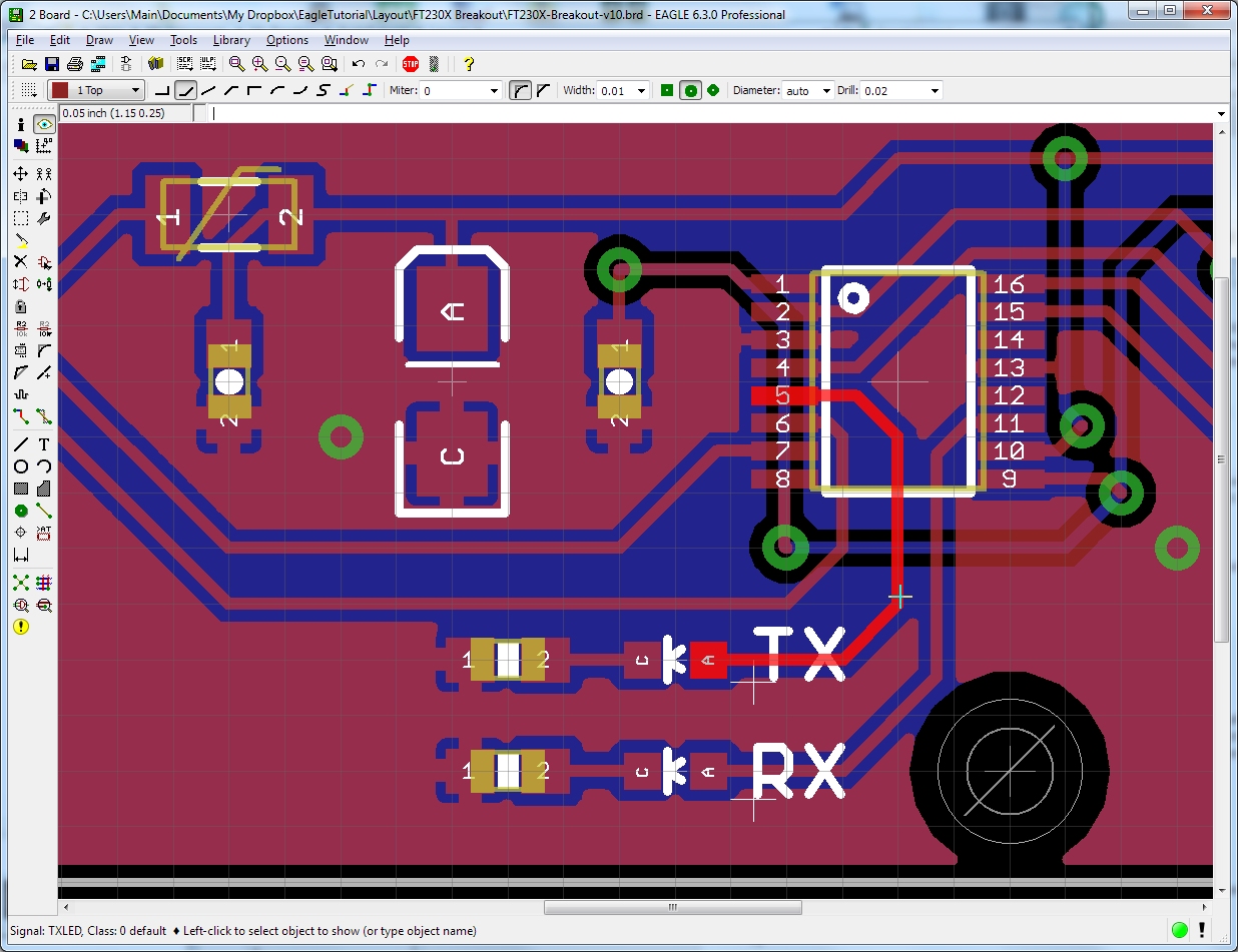
Rerouted. Now press F12 to ‘Show’ trace names and click on a trace. You will see the name of the net in the lower left corner of the Eagle window. ‘TXLED’ is now labeled correctly.
Copy the TX label a bunch more times. Press F12 and click on each trace to figure out what is there (Remember when we named the nets on the schematic? Here’s where it pays off). Then do a ‘Change’ wrench -> Text and change each label to what each pin actually is.
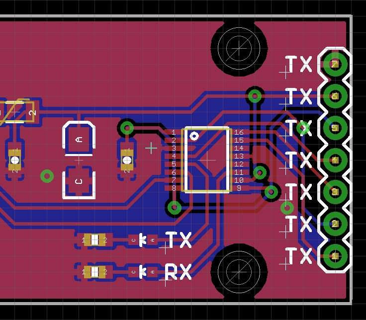
Is the text size a little too large for your taste? You can use the wrench to change 'size' as well. We prefer 0.05" or larger so that the text is easier to read.
Remember: the PCB fab house has limits to what it can do. We've found that anything smaller than 0.04" turns into an unreadable white blob.
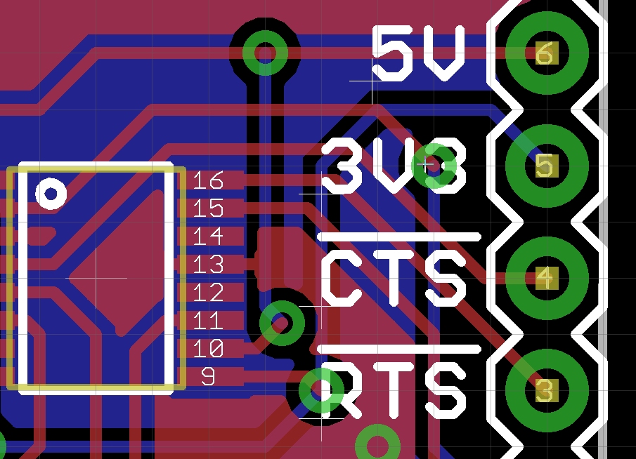
Now do some label centering. See those vias in the middle of the labels? The user will probably be able to read the label, but let’s move the two vias in order to make the label unbroken.
Is moving vias out of the way of text unnecessary? I would argue it is necessary. The board only has value if you know how to hook up to it. And I'm not talking about in the next week or two, I'm talking about when you're soldering on a ladder using a head lamp and you're not sure which spot to solder the sensor to... Clear labels make or break a project.
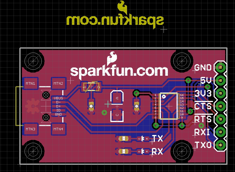
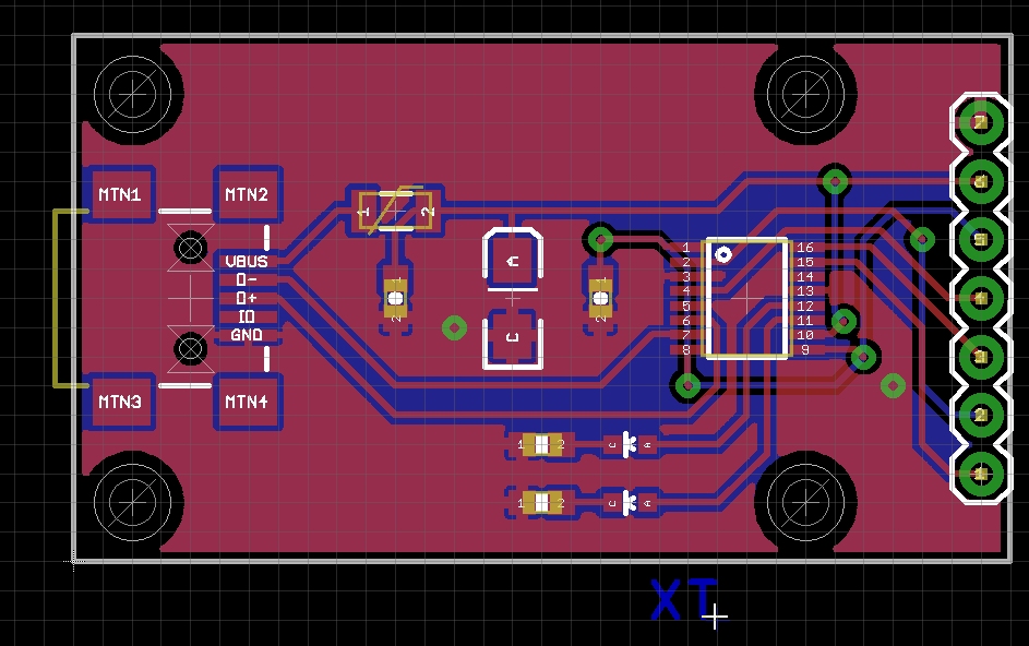
I am getting pretty happy with this layout. Let’s add some finishing touches. Because we’re SparkFun, we throw our logo on everything. We’re also a big proponent of the Open Source Hardware initiative. From the Aesthetics library, let’s add two of the LOGO-SFE and one OSHW-LOGO.
I sometimes have to add some lines on the tDocu layer to show me center point on the board. I draw these in by hand then remove them once I’ve used them to center a logo or text label.
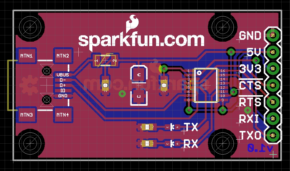
This is version v1.0 of the board so add that text, in copper, to the bottom of the board. Hit F8 to ratsnest refresh and see the text in the bottom copper.
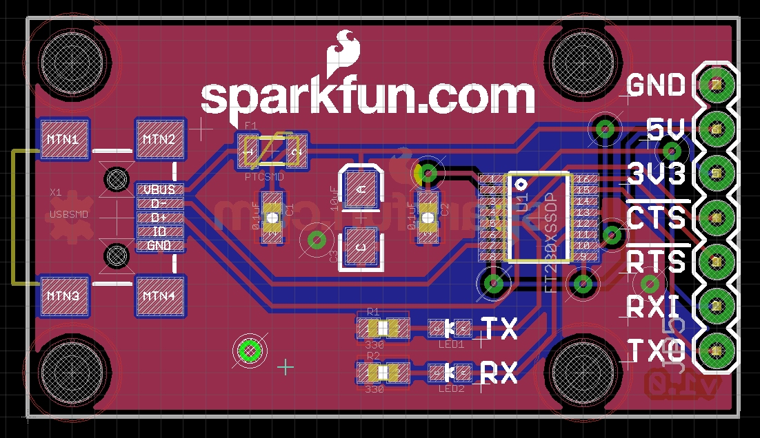
Now for some sanity checking. I’ve turned on all the layers to be sure that the vias will be tented (covered up by the solder mask). You can see in the screenshot that there are white hash marks on most SMD pads and on the large 0.1” connector on the end of the board. The smaller vias however do not have these hash marks. The DRC rules are set up (see the Mask tab under DRC) to mask over any hole 0.020” or smaller. I’ve added a larger via to show this point. This larger via would be exposed.
There are a few circumstances where we expose a via or two - usually for test points. We use a spring loaded pogo pin to make contact with that point on the board so that we can test the board more easily. But in general, all the vias on SparkFun boards are masked over for aesthetic reasons.
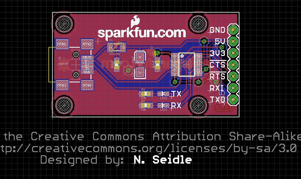
Lastly, we add the designer’s name to the PCB and schematic. This is to maintain attribution whenever the design gets reused or modified. It’s also nice to know who to talk to if there are support questions.