Using EAGLE: Schematic
Wiring Up the Schematic
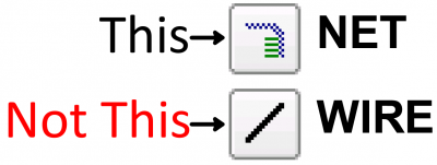
With all of the parts added to our schematic, it's time to wire them together. There's one major caveat here before we start: even though we're wiring parts on the schematic, we not going to use the WIRE tool --  -- to connect them together. Instead, we'll use the NET tool --
  (left toolbar, or under the Draw menu). The WIRE tool would be better-named as a line-drawing tool, NET does a better job of connecting components.
Using the NET Tool
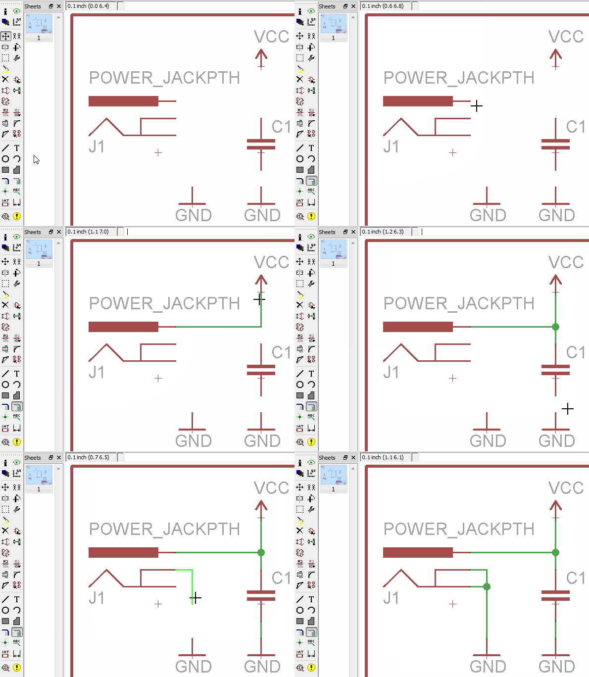
To use the NET tool, hover over the very end of a pin (as close as possible, zoom in if you have to), and left-click once to start a wire. Now a green line should be following your mouse cursor around. To terminate the net, left-click on either another pin or a net.
The hard part, sometimes, is identifying which part on a circuit symbol is actually a pin. Usually they're recognizable by a thin, horizontal, red line off to the side of a part. Sometimes (not always) they're labeled with a pin number. Make sure you click on the very end of the pin when you start or finish a net route.
Route the Power Input Circuit
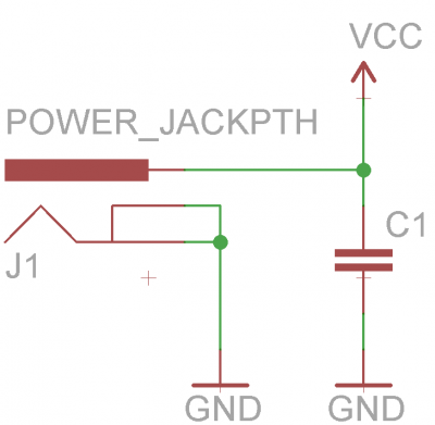
Start back in the upper left, and route the power input circuit like so:
Whenever a net splits in two directions a junction node is created. This signifies that all three intersecting nets are connected. If two nets cross, but there's not a junction, those nets are not connected.
Route the ATmega328 Circuit
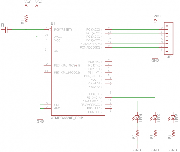
Next we'll route the ATmega328 to its supporting circuitry. There's LEDs, a connector, resistor, capacitor and VCC/GND symbols to route to:
Don't forget to add nets between the LEDs, resistors, and GND symbols!
Making Named, Labeled Net Stubs
The remaining nets we have to make are not going to be as easy to cleanly route. For example, we need to connect the TXO pin on JP2 to the ATmega's RXD pin, all the way on the other side. You could do it, it would work, but it'd be really ugly. Instead, we'll make net "stubs" and give them unique names to connect them.
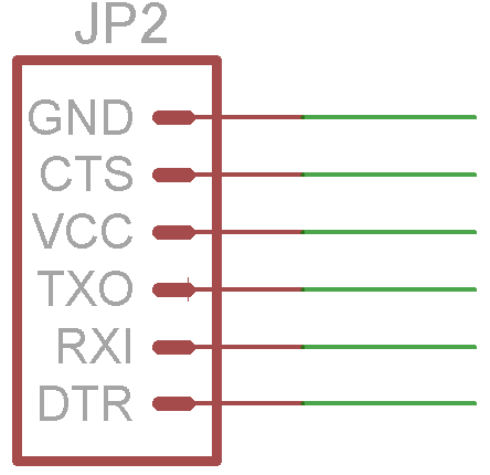
We'll start by adding short, one-sided nets to each of the six pins on the serial connector. Begin by starting a net at a pin, just as you've been doing. Terminate the net by left-clicking a few grid-lengths over to the right of the pin. Then, instead of routing to another pin, just hit ESC to finish the route. When you're done, it should look like this:
Next, we'll use the NAME tool --  (left toolbar, or under the Edit menu) -- to name each of the six nets. With the NAME tool selected, clicking on a net should open a new dialog. Start by naming the net connected to the top, GND pin. Delete the auto-generated name (e.g. N$14), and replace it with "GND" (sans the quotation marks). This should result in a warning dialog, asking you if you want to connect this net to all of the other nets named "GND" (that would be every net connected to a GND symbol). Thanks for looking out for us EAGLE, but in this case Yes we do want to connect GND to GND.
After naming a net, you should use the LABEL tool --  -- to add a text label. With the LABEL tool selected, left-click on the net you just named. This should spawn a piece of text that says "GND", left-click again to place the label down right on top of your net.
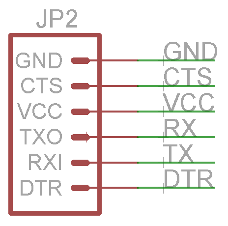
Follow that same order of operations for the remaining five net stubs. In the end, they should look like this (note the net connected to the TXO pin is named "RX", and a "TX" net connects to RXI -- that's on purpose):
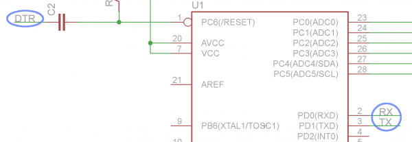
VCC should be the only other net that warns you that you'll be connecting to other nets named "VCC" (anything connected to a VCC voltage node). For the other named nets, we'll need to create this same stub somewhere else. Where exactly? Well, we need to add a "RX" and "TX" net on the ATmega328, and a "DTR" nearby as well:
Even though there's no green net connecting these pins, every net with the same, exact name is actually connected.
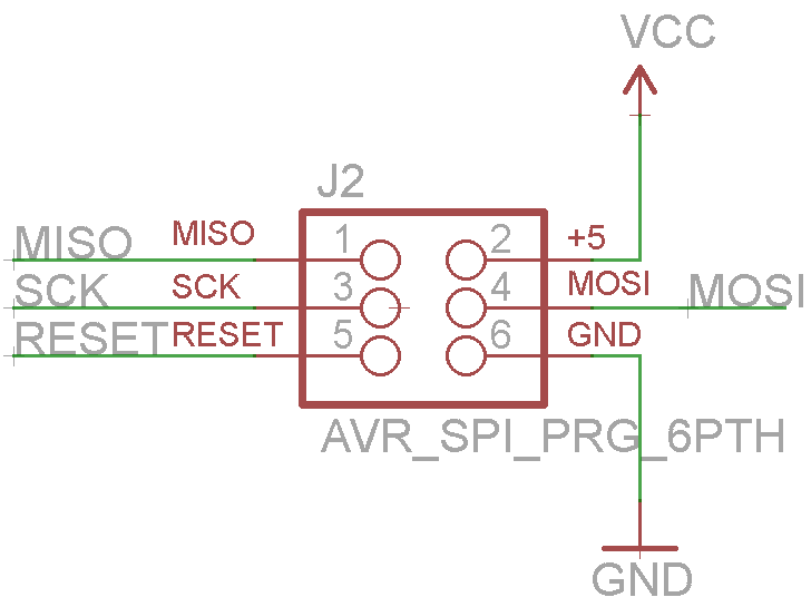
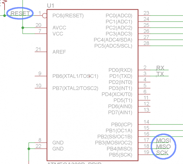
We need to do a lot of the same to connect the 2x3 programming header to the ATmega328. First, wire up the connector like so (naming/labeling MOSI, MISO, SCK, and RESET):
Then, back to the ATmega328, add the same four named/labeled nets:
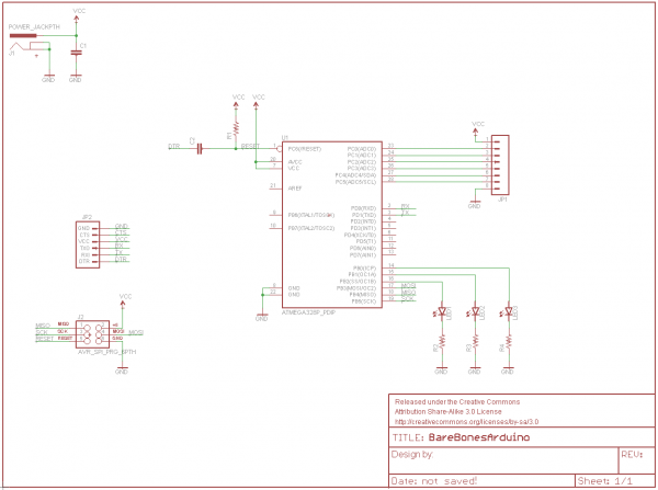
Phew -- you're done. Get excited, it's about time to lay out a PCB! When your schematic is done, it should look a little something like this:
The schematic layout is done, but there are a few tips and tricks we'd like to share before moving over to the PCB layout portion of the tutorial.
