SX1509 I/O Expander Breakout Hookup Guide
 jimblom
SX1509 Breakout Board Overview
There's a lot going on on the SX1509 Breakout. GPIO and power buses are broken out in every-which direction, and configurable jumpers cover most of the rest of the board.
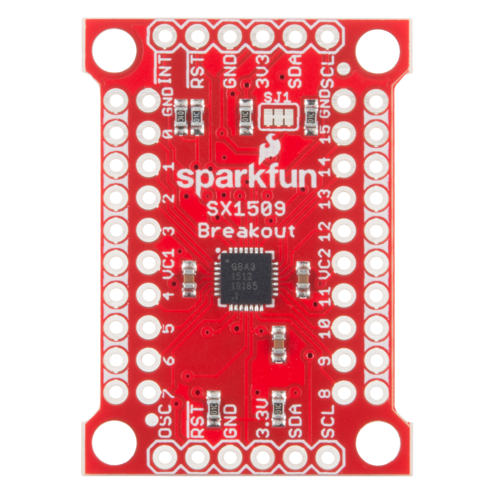
This section will cover all things SX1509 Breakout, so you can get the most out of the board's features.
I2C and Power Input Headers
These two headers at the top and bottom of the breakout board are the input and control headers to the board. This is where you can supply power to the SX1509, and where your I2C signals -- SDA and SCL -- will terminate.
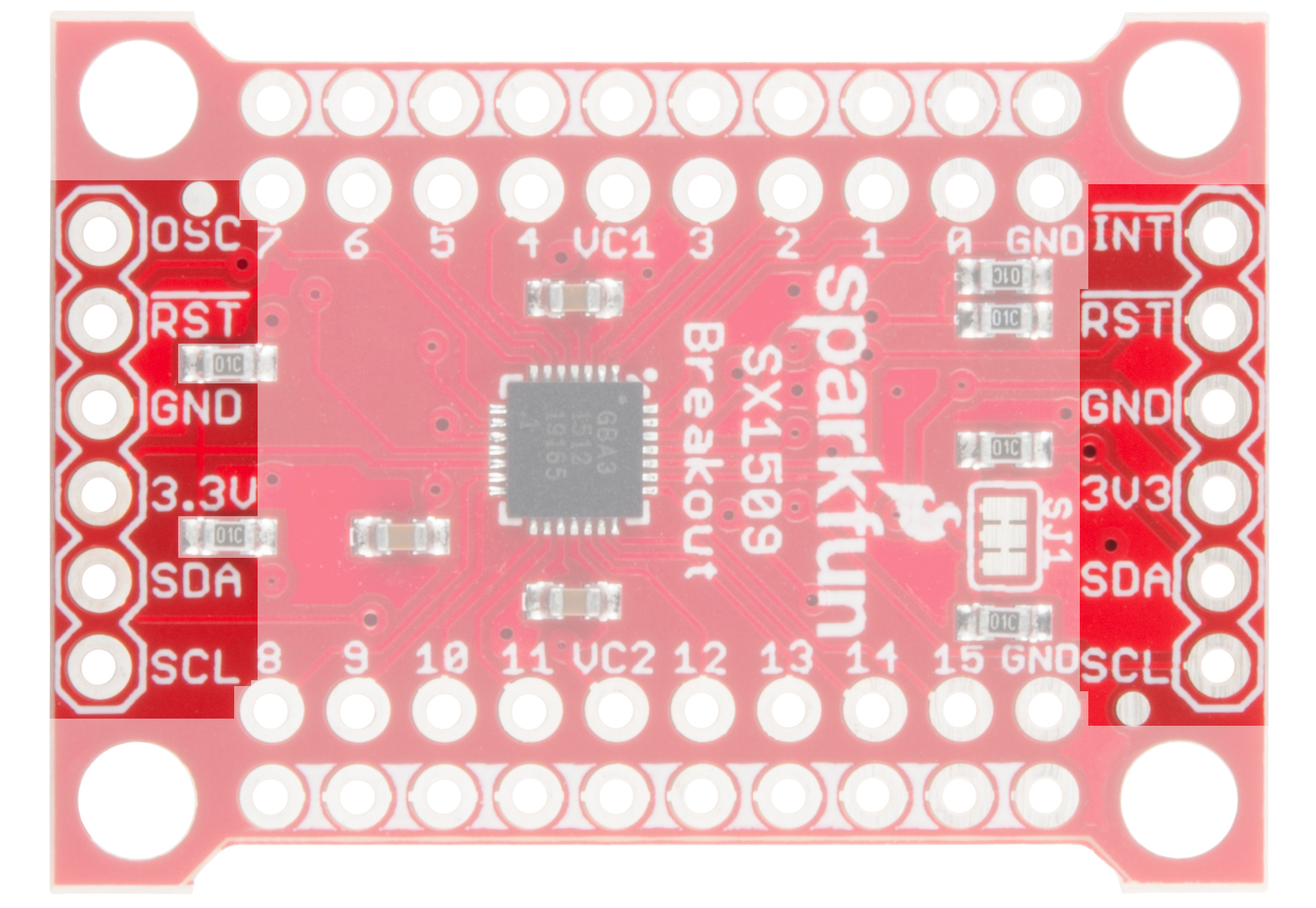
These headers break out the following pins:
| Pin Label | Type | Description |
|---|---|---|
| INT | Output | Active low programmable interrupt |
| RST | Input | Active low reset (pulled high on-board) |
| GND | Power | Ground (0V) |
| 3V3 | Power | Main supply voltage (1.425-3.6V) |
| SDA | I2C | I2C serial data line |
| SCL | I2C | I2C serial clock line |
| OSC | Clock In/Out | Optional clock input, or programmable clock signal output |
The SDA and SCL pins each have 10kΩ resistors pulling them up to 3.3V. These resistors can be disconnected by cutting the SJ1 jumpers.
RST -- the SX1509's active-low reset input -- works just like an Arduino reset pin. If the pin is pulled LOW, the SX1509 will power down. When RST rises, the SX1509 will turn back on, but all of its settings will be cleared out. The breakout board includes a 10kΩ resistor pulling RST HIGH, so you ignore this pin if you don't need the reset functionality.
INT is a very handy interrupt output, especially if you're using any SX1509 pins as inputs. It can be configured to go LOW whenever a pin state changes. The breakout board includes a 10kΩ resistor pulling INT HIGH.
Finally, OSC breaks out the SX1509's OSCIO pin -- the oscillator input/output. This highly-configurable pin can be used as either the clock input for the SX1509 (if you don't want to use its internal 2MHz clock), a clock output (producing an up to 2MHz square wave signal), or a simple digital I/O.
I/O and GND/VCC Breakouts
The real meat of the breakout board are the pairs of rows breaking out all sixteen I/O pins plus the power rails.
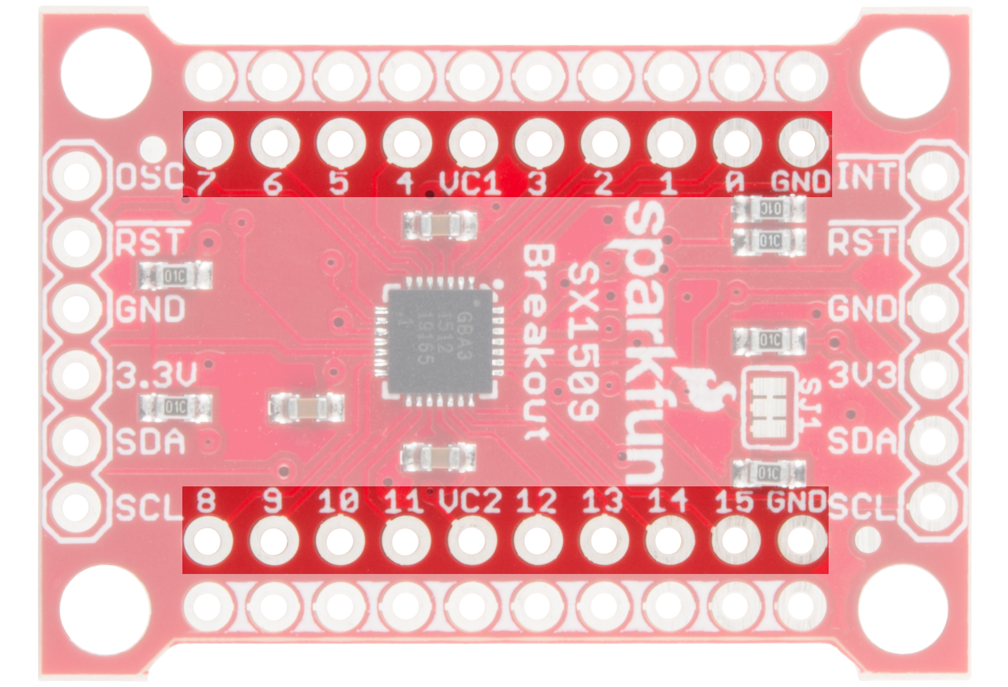
The SX1509 breaks its 16 I/O into two banks -- bank A and bank B. Each bank can operate on a separate power supply, but by default they're both set to 3.3V. Bank A is powered by VCC1, and bank B is supplied by VCC2. VCC1 and VCC2 can range between 1.2V and 3.6V, if you want to supply them externally. Check out the "Jumpers" section for more information on that.
Every I/O pin is capable of PWM and blink outputs, but only half of them can be set to "breathe" (blink with smooth transitions from on to off). Also, if you plan on using the SX1509 keypad driver, each I/O is relegated to either a row or column interface.
| LED Driver | Keypad | ||||
|---|---|---|---|---|---|
| I/O | PWM | Blink | Breathe | Row | Column |
| 0 | ✓ | ✓ | ✓ | ||
| 1 | ✓ | ✓ | ✓ | ||
| 2 | ✓ | ✓ | ✓ | ||
| 3 | ✓ | ✓ | ✓ | ||
| 4 | ✓ | ✓ | ✓ | ✓ | |
| 5 | ✓ | ✓ | ✓ | ✓ | |
| 6 | ✓ | ✓ | ✓ | ✓ | |
| 7 | ✓ | ✓ | ✓ | ✓ | |
| 8 | ✓ | ✓ | ✓ | ||
| 9 | ✓ | ✓ | ✓ | ||
| 10 | ✓ | ✓ | ✓ | ||
| 11 | ✓ | ✓ | ✓ | ||
| 12 | ✓ | ✓ | ✓ | ✓ | |
| 13 | ✓ | ✓ | ✓ | ✓ | |
| 14 | ✓ | ✓ | ✓ | ✓ | |
| 15 | ✓ | ✓ | ✓ | ✓ | |
Ground (or Power) Rails
Running alongside the I/O breakouts are a pair of power rails. These rails can be distinguished by the bars of white silkscreen running between each pad.

By default, these rails are both set to ground -- handy if you want to fan out some active-low buttons, or current-sourced LEDs. Jumpers on the back side allow you to switch the rails from GND to either VCC1 or VCC2. You'll need to cut the jumper between GND and the rail, then blob solder between the rail and VCC.
This bus is completely optional. Just don't solder male pins into both rows of headers if you plan on using the breakout in a breadboard!
Address-Select Jumpers
Up to four SX1509's can be connected to a single I2C bus, by configuring them to different addresses. The SX1509 has two pins devoted to I2C address selection: ADD0 and ADD1. Each of those pins are broken out to a jumper on the bottom of the board.
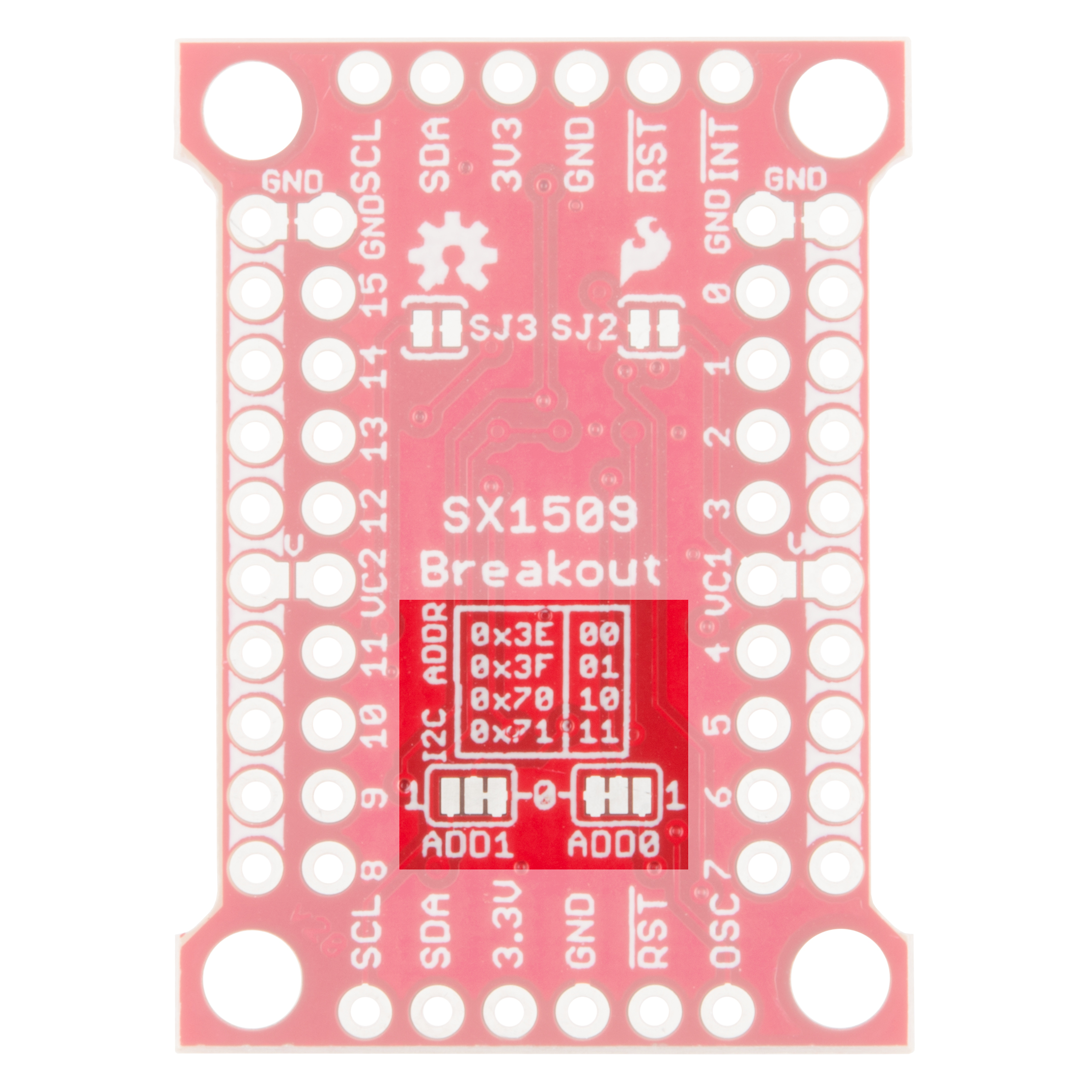
The board defaults each of those pins to GND, which sets the I2C address to 0x3E. To set either jumper to "1" (HIGH), grab a hobby knife, cut the trace connecting to "0", and blob some solder between the center pad and "1".
The four configurable addresses are listed on the back of the board, but for quick reference, they are:
| ADD1 | ADD0 | I2C address |
|---|---|---|
| 0 | 0 | 0x3E |
| 0 | 1 | 0x3F |
| 1 | 0 | 0x70 |
| 1 | 1 | 0x71 |
VCC1 and VCC2 Jumpers
SJ2 and SJ3 on the back-side of the board connect VCC2 and VCC1, respectively, to the 3V3 voltage supply input. So, if you're delivering 3.3V to the board, each of the I/O banks will operate at 3.3V.
If you want to take advantage of the SX1509's level-shifting capabilities by powering these banks at something other than VCC, cut the jumpers and plug any voltage between 1.2V and 3.6V into the VCC1 and/or VCC2 pins.
These supply buses are completely independent -- so they can operate at different voltages.