SparkFun Clock Generator 5P49V60 (Qwiic) Hookup Guide
 Elias The Sparkiest
Hardware Overview
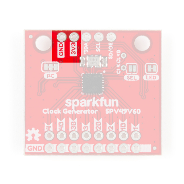
Power
Power can be supplied through the header along the top side of the board labeled 3.3V and GND. Alternatively, power can be supplied through the Qwiic connectors on either side of the board.
 |
 |
| Top View of Input Power | Bottom View of Qwiic Connectors |
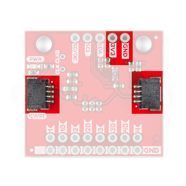
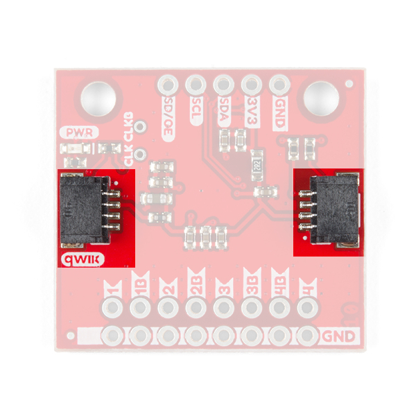
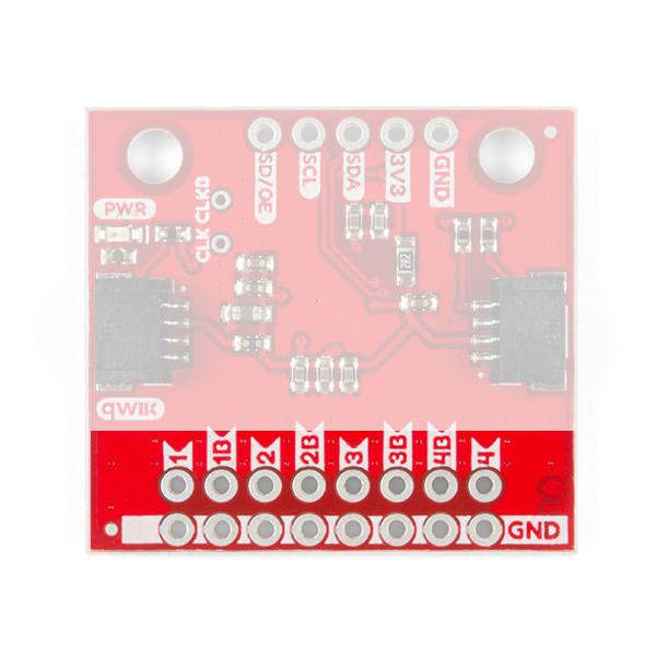
Qwiic Connectors
There are two Qwiic connectors on either end of the SparkFun Clock Generator to provide power and I2C connectivity simultaneously. The I2C address of the board is 0x6A by default [ 1 ]. The address can be changed to 0x68 using the library. The Qwiic ecosystem is made for fast prototyping by removing the need for soldering I2C data lines. However, in this case soldering is required to connect to the clock outputs.
0.
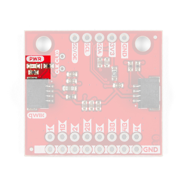
LED
There's a single red power LED, labeled PWR, on the bottom side of the board which indicates power is being supplied to the board.
Jumpers
There are three jumpers on the SparkFun Clock Generator.
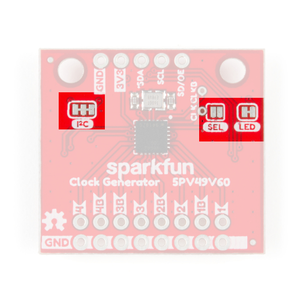
LED
Let's start with the jumpers on the right side of the board. The jumpers labeled LED can be cut to disconnect the red power LED so that it doesn't come on when power is supplied to the board. Not sure how to cut a jumper? Read here!
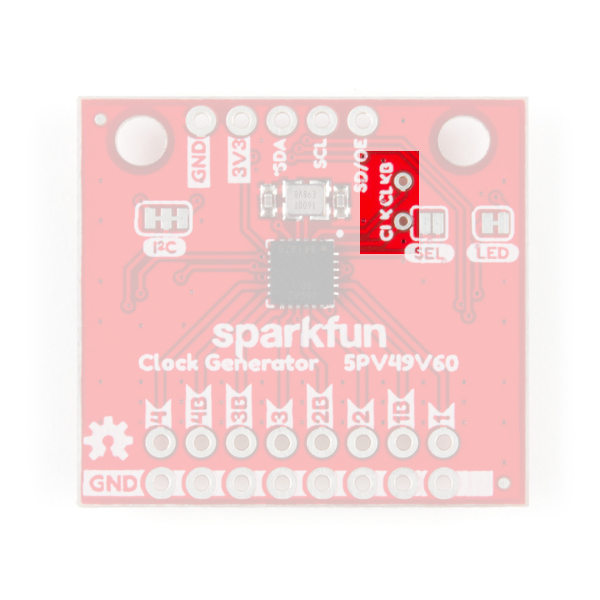
SEL
The second jumper labeled SEL enables the ability to load settings from the SparkFun's Clock Generators' One Time Programming memory banks. This disables the I2C data communication, turning those lines into selection pins. More information can be found down further under One Time Programming.
I2C
Finally, the jumpers labeled as I2C can be cut to disable the pull-up resistors on the I2C bus. In general, you shouldn’t need to mess with this jumper. But if you have many devices on your I2C bus, you may want to remove these resistors by cutting the two small traces between the solder pads.
Headers
There are two rows of headers on the SparkFun Clock Generator: one set contains all of the clock outputs while the other has I2C and a Shutdown/Output Enable Pin. There are also two pins just off-center of the board where a clock signal can be supplied to the board in place of the SparkFun Clock Generator's crystal.
Clock Output
The clock output header is located at the bottom of the board. There are four possible clock signals with four complementary signals for differential clock transmission. Each set of outputs, 1-4B, has it's own frequency output divider that allows for customizable outputs. Below are example sketches for SparkFun's Arduino Library that demonstrates how to easily set these frequencies.
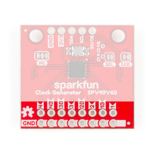 |
 |
| Top View of Clock Output | Bottom View of Clock Output |
I2C
On the opposite edge from the clock output header is header for I2C and a pin labeled SD/OE. The software configurable pin labeled SD/OE stands for "Shutdown/Output Enable" and serves a dual purpose of shutting down the IC or turning on and off the clock outputs. By default this pin acts as an output enable, disabling the clocks when held low. In the SparkFun Arduino Library, you can use the function: sdInputPinControl(byte control) to enable shutdown instead.
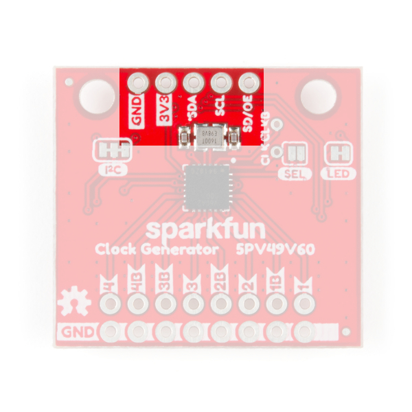 |
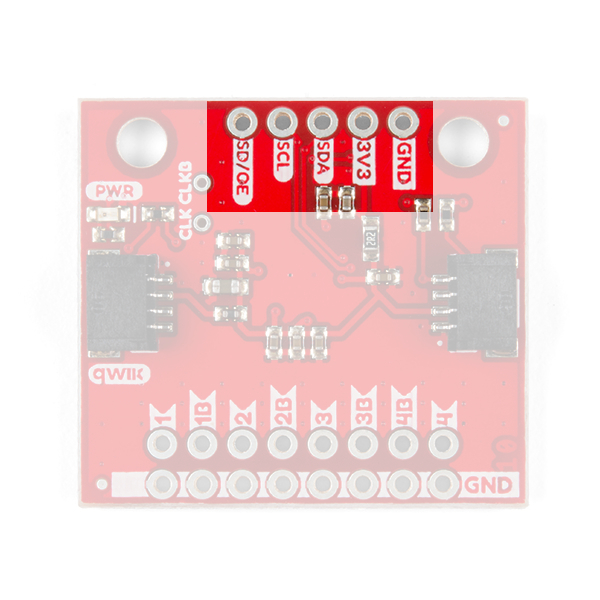 |
| Top View of I2C and Shutdown/Output Enable Pins | Bottom View of I2C and Shutdown/Output Enable Pins |
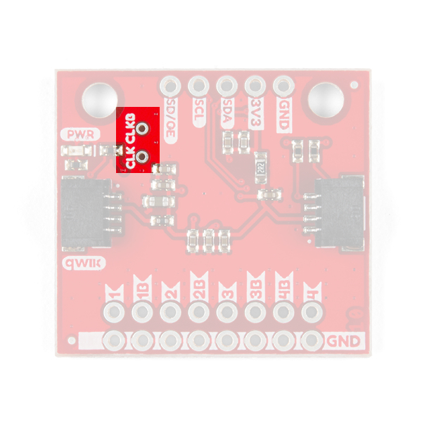
Alternate Clock Input Header
Just to the right of the SparkFun Clock Generator's Crystal - the little silver box just above the main IC, are two small holes labeled CLKIN and CLKINB. Using this small header it's possible to feed the SparkFun Clock Generator an external reference clock in place of the on-board crystal. There are two pins, but CLKIN can be used exclusively for single ended clock input. There is an Arduino example below that demonstrates how to enable this feature in code but more information on the hardware connectivity can be found on page 20 of the datasheet.
 |
 |
| Top View w/ Clock Input Header | Bottom View w/ Clock Input Header |
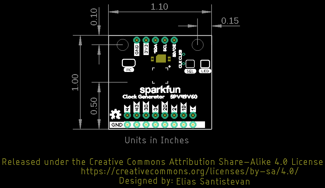
Board Dimensions
The overall board size is 1.10"x1.00". There are two mounting holes available on the board.
Clock Output Frequency
The SparkFun Clock Generator generates frequencies by using the small onboard crystal just above the IC in the center, as a reference clock. The diagram shown below from the datasheet displays how this works internally.
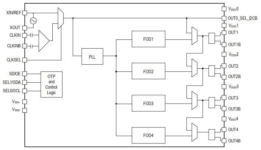
The reference clock (upper left two topmost pins) is manipulated internally in a phase lock loop (PLL center) to generate a frequency for the output dividers (FOD 1-4). These output dividers then set the frequencies for their respective clock outputs. These outputs are capable of frequencies between 1MHz-200MHz for single ended output or 1MHz-350MHz for differential signal output (see table in next section for specifics). It is possible to get even lower frequencies by feeding the output of one clock to the output divider of another clock in software. This is demonstrated in Arduino Example 6: Multiplex Clock Output below.
Each output divider for each clock is synchronized to maintain a low skew rate (phase of each clock) which can be programatically manipulated. In addition, the slew rate (rise and fall times) for each clock can also be set with one of four settings (see table below). Finally, a spread spectrum can be applied to the clock to reduce it's EMI or to increase it's robustness.
For each clock signal a corresponding signal type must be selected and proper hardware terminations must be applied accordingly. This is explained with some detail in the next section.
Slew rate
Below is the possible slew rate settings for the output frequencies at 3.3V.
| Slew Rates - 3.3V | |||
|---|---|---|---|
| Library Constant | Minimum | Typical | Units |
SLOWEST
|
1.0 | 2.2 | V/ns |
SLOW
|
1.2 | 2.3 | V/ns |
FAST
|
1.3 | 2.4 | V/ns |
FASTEST
|
1.7 | 2.7 | V/ns |
Signal Types and Termination
The SparkFun Clock Generator outputs different types of clock signals that each require their own specific hardware terminations. The following transmission outputs are available:
| Single Ended Output | Differential Signal Output | |
|---|---|---|
| Frequency Range | 1MHz - 200MHz | 1MHz - 350MHz |
| CMOS | LVPECL | |
| CMOS2 | LVDS | |
| CMOSD | HCSL33 |
In addition, transmission of these signals require ~50Ω trace impedance to avoid attenuation and distortion of the clock signal. Towards this goal, the board has been designed with 60Ω trace impedance with the shortest length possible between the header and the IC. The difference between the ideal trace and the Sparkfun Clock Generator's impedance can be remedied with series resistors or proper terminations and may not even be an issue depending on the selected frequency.
The selected signal type will require a different hardware termination. Below are the hardware terminations found in the 5P49V60 Clock Generator's datasheet.
| Signal Type | Hardware Termination |
|---|---|
| LVCMOS | 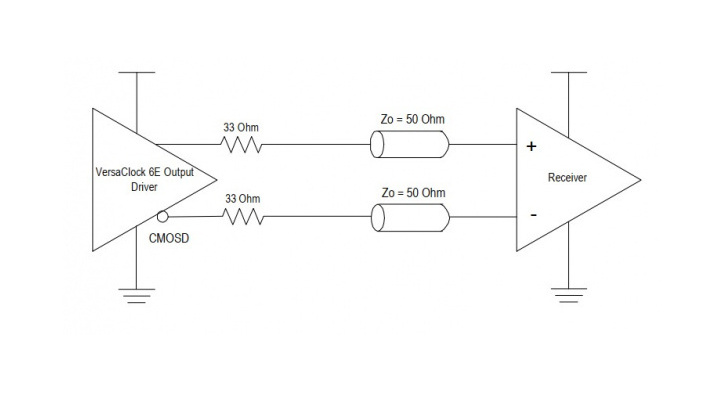
|
| LVPECL | 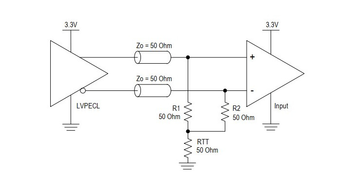
|

|
|
| LVDS | 
|
| HCSL33 Driver | 
|
| HCSL33 Source | 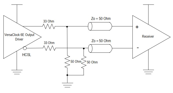
|
One Time Programming (OTP)
The SparkFun Clock Generator can save all of the programmed settings to any of its four programmable banks of RAM. However, keep in mind that this RAM can only be programmed once (One Time Programmable)! After programming any of the banks of memory, it's possible to select which bank is loaded (0-3) when the SparkFun Clock Generator powers up. This is done by closing the SEL jumper and using the pin labeled SCL as "select zero" and SDA as "select one". Using these pins like two bits will select the corresponding bank, see table below.
| Select 0 (SCL) | Select 1 (SDA) | Bank |
|---|---|---|
| 0 | 0 | 0 |
| 0 | 1 | 1 |
| 1 | 0 | 2 |
| 1 | 1 | 3 |
A detailed list of steps on how to accomplish programming these banks can be found on page 5 of the programming guide.