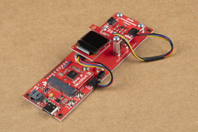
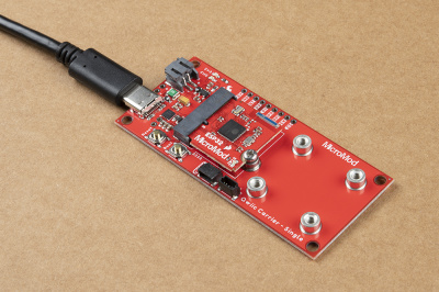
Qwiic Carrier Board Hookup Guide
Introduction
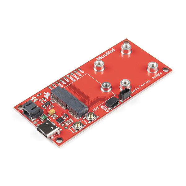
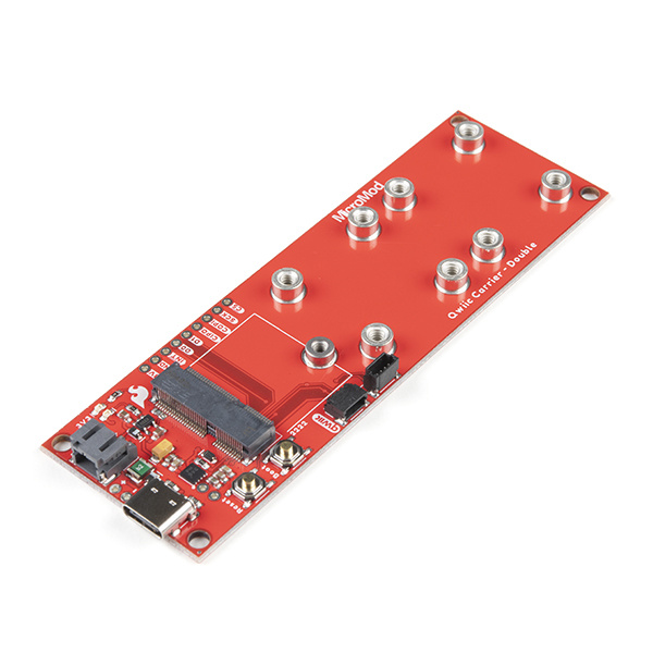
The MicroMod Qwiic Carrier Board can be used to rapidly prototype with other Qwiic devices; it is available in either a single or double mounting configuration. Just like other MicroMod Carrier Boards, users are free to develop with MicroMod Processor Board of their choice.
For a quick overview, check out our product video showcasing the MicroMod Qwiic carrier boards:
Required Materials
To get started, users will need a few of items listed below. (You may already have a some of these items; read through the guide and modify your cart accordingly.)
MicroMod Processor Board
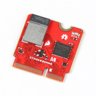
Like other MicroMod Carrier Boards, a Processor Board is required for the product to operate. Users will need a Processor Board (of their choice) to attach to the MicroMod M.2 connector; since, one is not included with this product. Below, are few options:
Required Hardware
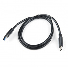
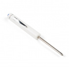
A Phillips screw driver is necessary to attach the Processor board to the Carrier Board. Additionally, a USB-C cable is needed to connect the Carrier Board to a computer.
Optional Hardware
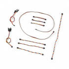
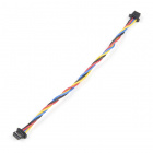
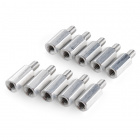
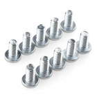
To connect Qwiic breakout boards for your MicroMod project, Qwiic cables are required. Users can also attach the Qwiic devices with 4-40 screws or stacked them with standoffs.
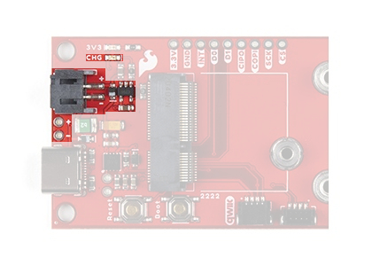
A single-cell Lithium-ion battery can be connected to the Qwiic Carrier Board for portability.
Lithium Ion Battery - 1Ah
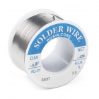
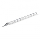
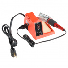
PRT-13813To modify the jumpers, users will need soldering equipment and/or a knife.
Weller WLC100 Soldering Station
TOL-14228Suggested Reading
The MicroMod ecosystem is a unique way to allow users to customize their project to their needs. The Qwiic connect system is a simple method for interfacing with I2C devices. Click on the banners below for more information on each system.
For users who aren't familiar with the following concepts, we also recommend reading the following tutorials before continuing.
Serial Communication
I2C
Getting Started with MicroMod
Designing with MicroMod
Installing an Arduino Library
Installing Arduino IDE
Installing Board Definitions in the Arduino IDE
Hardware Overview
This section will cover the various hardware components and solder jumpers on the MicroMod Qwiic Carrier Board. It will also review the connections of the M.2 connector and how it interfaces with a MicroMod Processor.
Board Dimensions
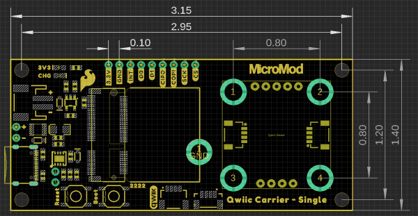
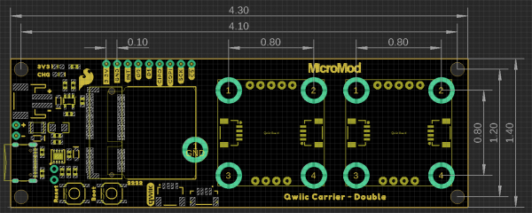
The Qwiic Carrier Board dimensions are:
- Single: 3.15" x 1.40" (80.00mm x 35.56mm)
- Double: 4.10" x 1.40" (109.22mm x 35.56mm)
The boards also include mounting holes and inserts for a standard 4-40 screw. The inserts are arranged to mount, attach, and/or stack compatible (1" x 1") Qwiic boards.
Common Components
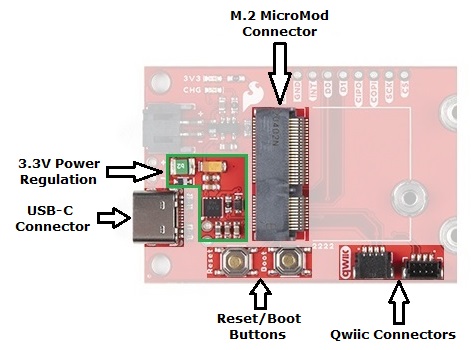
Most SparkFun MicroMod Carrier Boards will have some common components and all MicroMod Carrier Boards will have the keyed M.2 MicroMod connector for a Processor board. The photo and list below outline the common components between the Qwiic carrier board and other MicroMod Carrier Boards.
- M.2 MicroMod Connector - This special keyed M.2 connector lets you install your MicroMod Processor of choice to the Qwiic Carrier Board.
- USB-C Connector - Connect to your computer to program your processor and provide power to the board.
- 3.3V Regulator - Provides a regulated 3.3V and sources up to 1A.
- Qwiic Connectors - The standard Qwiic connectors to connect other Qwiic devices for your MicroMod project.
- Boot/Reset Buttons - Push buttons to enter boot mode on processors and to reset your MicroMod circuit.
Battery Charger
The board also has a MCP73831 Single-Cell Lithium-Ion/Lithium-Polymer Charge IC so you can charge an attached single-cell LiPo battery. The charge IC receives power from the USB connection and can source up to 450mA to charge an attached battery.
Status LEDs
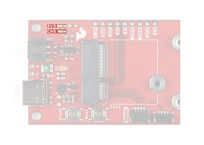
The carrier board has two status LEDs:
- PWR - This LED indicates when 3.3V power is available top the board.
- CHG - This LED indicates the status of the charging circuit operation.
Solder Jumpers
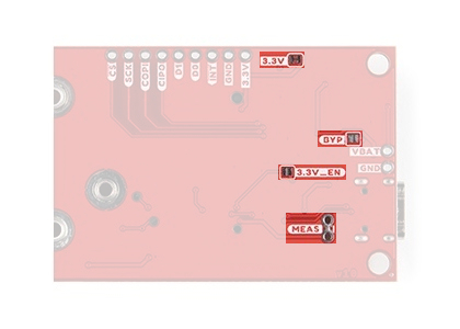
There are four adjustable solder jumpers on the MicroMod Qwiic Carrier Board labeled MEAS, BYP, 3.3V_VE and 3.3V. The table below briefly outlines their functionalities:
| Jumper Name/Label | Description | Default State |
|---|---|---|
| Measure/MEAS | Open this jumper to probe the current draw at the 3.3V output of the regulator. For help measuring current, take a look at our How to Use a Multimeter tutorial. | CLOSED |
| Bypass/BYP | The "penny-in-the-fuse" jumper. Bypasses the 6V/2A fuse and nets VIN and V_USB together. Close only if you know what you are doing! | OPEN |
| Voltage Regulator Enable/VE | Voltage regulator control. Close this jumper to control the VREG in low-power applications. | OPEN |
| 3.3V LED Power/3V3 LED | Connects the 3.3V LED to 3.3V via a 1K Ohm resistor. Open to disable the LED. | CLOSED |
MicroMod Pinout
Since this Carrier Board is designed to work with all of the MicroMod Processors we've included the table below to outline which pins are used so, if you would like, you can compare them to the pinout tables in their respective Hookup Guides.
| AUDIO | UART | GPIO/BUS | I2C | SDIO | SPI | Dedicated |
| Function | Bottom Pin |
Top Pin |
Function | ||||||
|---|---|---|---|---|---|---|---|---|---|
| (Not Connected) | 75 | GND | |||||||
| 3.3V | 74 | 73 | G5 / BUS5 | ||||||
| RTC_3V_BATT | 72 | 71 | G6 / BUS6 | ||||||
| SPI_CS1# | SDIO_DATA3 (I/O) | 70 | 69 | G7 / BUS7 | |||||
| SDIO_DATA2 (I/O) | 68 | 67 | G8 | ||||||
| SDIO_DATA1 (I/O) | 66 | 65 | G9 | ADC_D- | CAM_HSYNC | ||||
| SPI_CIPO1 | SDIO_DATA0 (I/O) | 64 | 63 | G10 | ADC_D+ | CAM_VSYNC | |||
| SPI COPI1 | SDIO_CMD (I/O) | 62 | 61 | SPI_CIPO (I) | |||||
| SPI SCK1 | SDIO_SCK (O) | 60 | 59 | SPI_COPI (O) | LED_DAT | ||||
| AUD_MCLK (O) | 58 | 57 | SPI_SCK (O) | LED_CLK | |||||
| CAM_MCLK | PCM_OUT | I2S_OUT | AUD_OUT | 56 | 55 | SPI_CS# | |||
| CAM_PCLK | PCM_IN | I2S_IN | AUD_IN | 54 | 53 | I2C_SCL1 (I/O) | |||
| PDM_DATA | PCM_SYNC | I2S_WS | AUD_LRCLK | 52 | 51 | I2C_SDA1 (I/O) | |||
| PDM_CLK | PCM_CLK | I2S_SCK | AUD_BCLK | 50 | 49 | BATT_VIN / 3 (I - ADC) (0 to 3.3V) | |||
| G4 / BUS4 | 48 | 47 | PWM1 | ||||||
| G3 / BUS3 | 46 | 45 | GND | ||||||
| G2 / BUS2 | 44 | 43 | CAN_TX | ||||||
| G1 / BUS1 | 42 | 41 | CAN_RX | ||||||
| G0 / BUS0 | 40 | 39 | GND | ||||||
| A1 | 38 | 37 | USBHOST_D- | ||||||
| GND | 36 | 35 | USBHOST_D+ | ||||||
| A0 | 34 | 33 | GND | ||||||
| PWM0 | 32 | 31 | Module Key | ||||||
| Module Key | 30 | 29 | Module Key | ||||||
| Module Key | 28 | 27 | Module Key | ||||||
| Module Key | 26 | 25 | Module Key | ||||||
| Module Key | 24 | 23 | SWDIO | ||||||
| UART_TX2 (O) | 22 | 21 | SWDCK | ||||||
| UART_RX2 (I) | 20 | 19 | UART_RX1 (I) | ||||||
| CAM_TRIG | D1 | 18 | 17 | UART_TX1 (0) | |||||
| I2C_INT# | 16 | 15 | UART_CTS1 (I) | ||||||
| I2C_SCL (I/0) | 14 | 13 | UART_RTS1 (O) | ||||||
| I2C_SDA (I/0) | 12 | 11 | BOOT (I - Open Drain) | ||||||
| D0 | 10 | 9 | USB_VIN | ||||||
| SWO | G11 | 8 | 7 | GND | |||||
| RESET# (I - Open Drain) | 6 | 5 | USB_D- | ||||||
| 3.3V_EN | 4 | 3 | USB_D+ | ||||||
| 3.3V | 2 | 1 | GND | ||||||
| Signal Group | Signal | I/O | Description | Voltage | Power | 3.3V | I | 3.3V Source | 3.3V |
|---|---|---|---|---|
| GND | Return current path | 0V | ||
| USB_VIN | I |
USB VIN compliant to USB 2.0 specification. Connect to pins on Processor Board that require 5V for USB functionality. |
4.8-5.2V | |
| RTC_3V_BATT | I |
3V provided by external coin cell or mini battery. Max draw = 100μA. Connect to pins maintaining an RTC during power loss. Can be left NC. |
3V | |
| 3.3V_EN | O | Controls the carrier board's main voltage regulator. Voltage above 1V will enable 3.3V power path. | 3.3V | |
| BATT_VIN/3 | I |
Carrier board raw voltage over 3. 1/3 resistor divider is implemented on carrier board. Amplify the analog signal as needed for full 0-3.3V range |
3.3V | |
| Reset | Reset | I | Input to processor. Open drain with pullup on processor board. Pulling low resets processor. | 3.3V |
| Boot | I | Input to processor. Open drain with pullup on processor board. Pulling low puts processor into special boot mode. Can be left NC. | 3.3V | |
| USB | USB_D± | I/O | USB Data ±. Differential serial data interface compliant to USB 2.0 specification. If UART is required for programming, USB± must be routed to a USB-to-serial conversion IC on the processor board. | |
| USB Host | USBHOST_D± | I/O | For processors that support USB Host Mode. USB Data±. Differential serial data interface compliant to USB 2.0 specification. Can be left NC. | |
| CAN | CAN_RX | I | CAN Bus receive data. | 3.3V |
| CAN_TX | O | CAN Bus transmit data. | 3.3V | |
| UART | UART_RX1 | I | UART receive data. | 3.3V |
| UART_TX1 | O | UART transmit data. | 3.3V | |
| UART_RTS1 | O | UART request to send. | 3.3V | |
| UART_CTS1 | I | UART clear to send. | 3.3V | |
| UART_RX2 | I | 2nd UART receive data. | 3.3V | |
| UART_TX2 | O | 2nd UART transmit data. | 3.3V | |
| I2C | I2C_SCL | I/O | I2C clock. Open drain with pullup on carrier board. | 3.3V |
| I2C_SDA | I/O | I2C data. Open drain with pullup on carrier board | 3.3V | |
| I2C_INT# | I | Interrupt notification from carrier board to processor. Open drain with pullup on carrier board. Active LOW | 3.3V | |
| I2C_SCL1 | I/O | 2nd I2C clock. Open drain with pullup on carrier board. | 3.3V | |
| I2C_SDA1 | I/O | 2nd I2C data. Open drain with pullup on carrier board. | 3.3V | |
| SPI | SPI_COPI | O | SPI Controller Output/Peripheral Input. | 3.3V |
| SPI_CIPO | I | SPI Controller Input/Peripheral Output. | 3.3V | |
| SPI_SCK | O | SPI Clock. | 3.3V | |
| SPI_CS# | O | SPI Chip Select. Active LOW. Can be routed to GPIO if hardware CS is unused. | 3.3V | |
| SPI/SDIO | SPI_SCK1/SDIO_CLK | O | 2nd SPI Clock. Secondary use is SDIO Clock. | 3.3V |
| SPI_COPI1/SDIO_CMD | I/O | 2nd SPI Controller Output/Peripheral Input. Secondary use is SDIO command interface. | 3.3V | |
| SPI_CIPO1/SDIO_DATA0 | I/O | 2nd SPI Peripheral Input/Controller Output. Secondary use is SDIO data exchange bit 0. | 3.3V | |
| SDIO_DATA1 | I/O | SDIO data exchange bit 1. | 3.3V | |
| SDIO_DATA2 | I/O | SDIO data exchange bit 2. | 3.3V | |
| SPI_CS1/SDIO_DATA3 | I/O | 2nd SPI Chip Select. Secondary use is SDIO data exchange bit 3. | 3.3V | |
| Audio | AUD_MCLK | O | Audio master clock. | 3.3V |
| AUD_OUT/PCM_OUT/I2S_OUT/CAM_MCLK | O | Audio data output. PCM synchronous data output. I2S serial data out. Camera master clock. | 3.3V | |
| AUD_IN/PCM_IN/I2S_IN/CAM_PCLK | I | Audio data input. PCM syncrhonous data input. I2S serial data in. Camera periphperal clock. | 3.3V | |
| AUD_LRCLK/PCM_SYNC/I2S_WS/PDM_DATA | I/O | Audio left/right clock. PCM syncrhonous data SYNC. I2S word select. PDM data. | 3.3V | |
| AUD_BCLK/PCM_CLK/I2S_CLK/PDM_CLK | O | Audio bit clock. PCM clock. I2S continuous serial clock. PDM clock. | 3.3V | |
| SWD | SWDIO | I/O | Serial Wire Debug I/O. Connect if processor board supports SWD. Can be left NC. | 3.3V |
| SWDCK | I | Serial Wire Debug clock. Connect if processor board supports SWD. Can be left NC. | 3.3V | |
| ADC | A0 | I | Analog to digital converter 0. Amplify the analog signal as needed to enable full 0-3.3V range. | 3.3V |
| A1 | I | Analog to digital converter 1. Amplify the analog signal as needed to enable full 0-3.3V range. | 3.3V | |
| PWM | PWM0 | O | Pulse width modulated output 0. | 3.3V |
| PWM1 | O | Pulse width modulated output 1. | 3.3V | |
| Digital | D0 | I/O | General digital input/output pin. | 3.3V |
| D1/CAM_TRIG | I/O | General digital input/output pin. Camera trigger. | 3.3V | |
| General/Bus | G0/BUS0 | I/O | General purpose pins. Any unused processor pins should be assigned to Gx with ADC + PWM capable pins given priority (0, 1, 2, etc.) positions. The intent is to guarantee PWM, ADC and Digital Pin functionality on respective ADC/PWM/Digital pins. Gx pins do not guarantee ADC/PWM function. Alternative use is pins can support a fast read/write 8-bit or 4-bit wide bus. | 3.3V |
| G1/BUS1 | I/O | 3.3V | ||
| G2/BUS2 | I/O | 3.3V | ||
| G3/BUS3 | I/O | 3.3V | ||
| G4/BUS4 | I/O | 3.3V | ||
| G5/BUS5 | I/O | 3.3V | ||
| G6/BUS6 | I/O | 3.3V | ||
| G7/BUS7 | I/O | 3.3V | ||
| G8 | I/O | General purpose pin | 3.3V | |
| G9/ADC_D-/CAM_HSYNC | I/O | Differential ADC input if available. Camera horizontal sync. | 3.3V | |
| G10/ADC_D+/CAM_VSYNC | I/O | Differential ADC input if available. Camera vertical sync. | 3.3V | |
| G11/SWO | I/O | General purpose pin. Serial Wire Output | 3.3V |
| M.2 Connector Pin# | MicroMod Pin Name | Board Connection | Description |
|---|---|---|---|
| 1 | GND | GND | Ground plane. |
| 2 | 3.3V | 3.3V | Regulated 3.3V via USB-C. |
| 3 | USB_D+ | -- | USB D+ connection for Processor Board. |
| 4 | 3.3V_EN | -- | Voltage regulator enable input. |
| 5 | USB_D- | -- | USB D- connection for Processor Board. |
| 6 | RESET | RESET Button | Connected to RESET Button. Reset is active LOW |
| 9 | USB_VIN | -- | Input voltage from USB. |
| 10 | D0 | D0 | Digital I/O pin |
| 11 | BOOT | BOOT Button | Connected to BOOT Button. Boot is active LOW. |
| 12 | I2C_SDA | Qwiic Connector - SDA | I2C data signal for Qwiic devices. |
| 14 | I2C_SCL | Qwiic Connector - SCL | I2C clock signal for Qwiic devices. |
| 16 | I2C_INT | INT | I2C interrupt pin |
| 18 | D1 | D1 | Digital I/O pin |
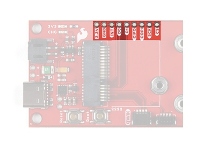
| 55 | SPI_CS | CS | Chip Select. |
| 57 | SPI_SCK | SCK | SPI Clock signal. |
| 59 | SPI_COPI | COPI | SPI Controller Out/Peripheral In signal. |
| 61 | SPI_CIPO | CIPO | SPI Controller In/Peripheral Out signal. |
Breakout Pins
The Qwiic Carrier Board features a 3.3V, a ground, seven I/O breakout pins. The functionality of these pins are detailed in the table above.
Hardware Assembly
For those unfamiliar with the MicroMod ecosystem, be sure to review the Getting Started with MicroMod guide.
Getting Started with MicroMod
Processor Board
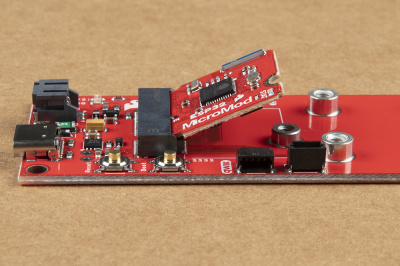
To get started with the Qwiic Carrier Board, users will need a compatible Processor. Insert the MicroMod Processor board into the M.2 socket at an angle, with its edge connector aligned to the matching slots.
When inserted properly, the Processor board will rest at an angle:
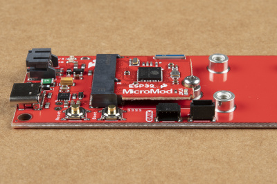
To secure the processor board, gently hold down on the board and attach the M.2 screw with a Phillip's head (PH0 or PH1) screw driver. Below, is an example of an assembled MicroMod system:
Qwiic Devices
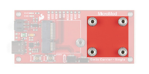
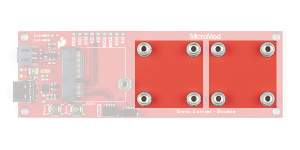
Screw inserts are available in either a single or double configuration to attach/mount 1" x 1" Qwiic devices to the Qwiic carrier board. The inserts are compatible with 4-40 screws; additionally, 4-40 3/8" standoffs can also be used to stack boards vertically.
To electronically connect the Qwiic devices to the Carrier Board, users will need Qwiic cables. For more information, check out our Qwiic ecosystem page.
Programming
To program the processor board utilized on the Qwiic Carrier Board; connect the board to a computer with a USB-C cable. Depending on the Processor board, user may need to install drivers (if they have not done so already).
Note: Make sure that the correct board definitions are installed in the Arduino IDE, for the selected Processor board. For help installing board definitions, use the MicroMod processor boards landing page and review the associated hookup guide for that hardware.
Installing Board Definitions in the Arduino IDE
Example
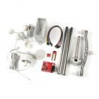
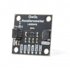
Below is a simple demonstration of using the MicroMod Qwiic Carrier Board to create a bubble level, using an accelerometer and OLED display. Users will also need other parts and accessories; all parts besides the Qwiic carrier board are listed below:
SparkFun Micro OLED Breakout (Qwiic)
LCD-14532Note: We have chosen the MicroMod ESP32 for the processor board for this demonstration; however, users are free to utilize the processor board of their choice.
Please note, that the sample code below is intended to program processor boards that are compatible with the Arduino IDE. Therefore, processor boards like the RP2040 are going to need extra effort to adapt the code (technical assistance for which, is not available).
Assembly
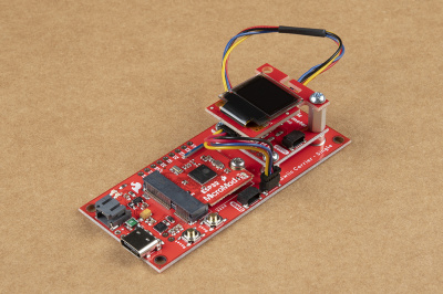
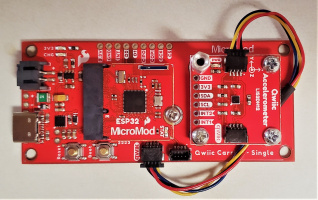
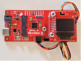
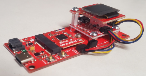
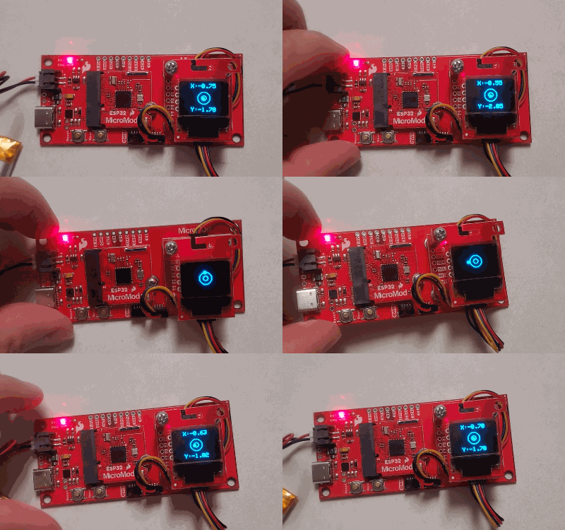
The assemble process is relatively straight forward. The primary thing that users need to pay attention to is the orientation of the OLED display relative to the axes of the accelerometer. The x-axis should point to the right of the OLED display and the y-axis should point to the top of the display (see images below).
Some users may find it the movement of the bubble in the example code to be more intuitive if the OLED display is stacked above the accelerometer.
Example Code
Users can download the example code here or by clicking the button below. Besides the RP2040 processor board, users only need to select the proper port and board from the board manager in the Arduino IDE before uploading the code.
The following sections break down the example code execution for users who might want to modify the code. Please note, as defined in our terms of service, that we do not provide technical assistance for any code modifications.
Dependencies
Below are the dependencies for the code including the libraries, pin definitions, and variable instantiations. The example code requires both the Micro OLED and LIS2DH12 Arduino libraries to be installed in the Arduino IDE.
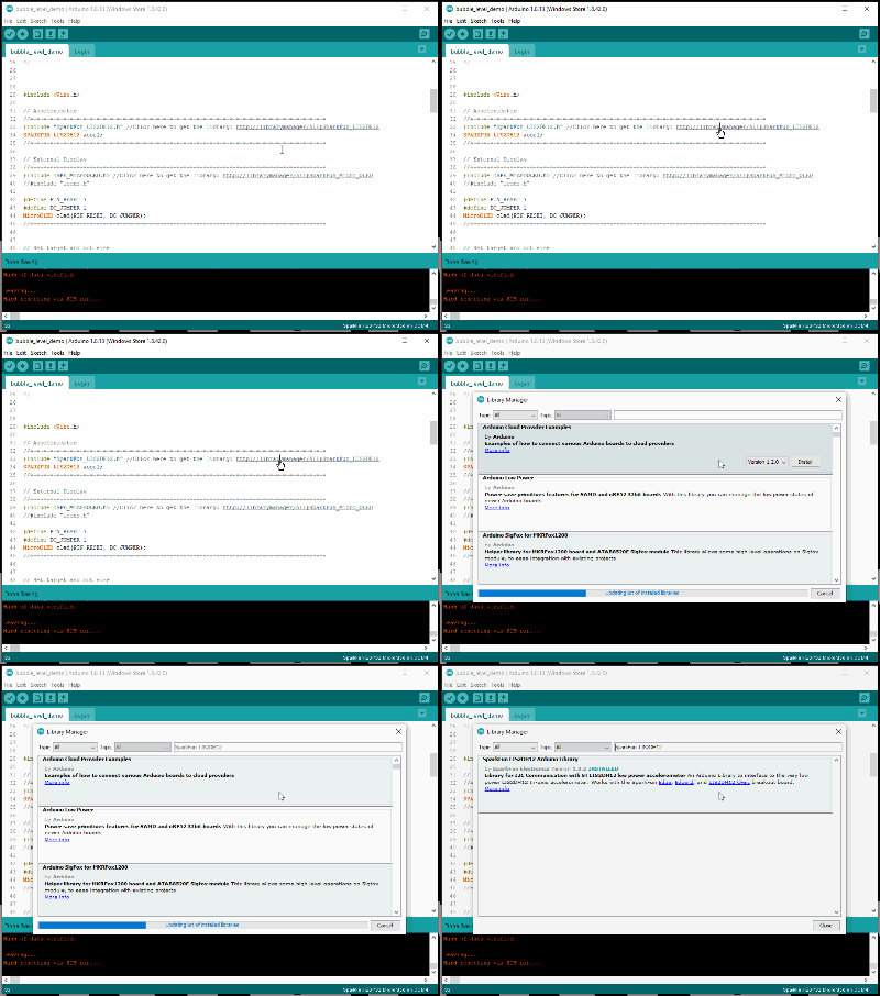
Tip: While in the Arduino IDE, users can click the links in the code (i.e. //Click here to get the library: http://librarymanager/All#SparkFun_LIS2DH12) to pull up the required library in the library manager.
Installing an Arduino Library
Libraries and Pin Definitions
This section of the code contains the required libraries and pin definitions for the code.
language:c
#include <Wire.h>

// Accelerometer
//=-=-=-=-=-=-=-=-=-=-=-=-=-=-=-=-=-=-=-=-=-=-=-=-=-=-=-=-=-=-=-=-=-=-=-=-=-=-=-=-=-=-=-=-=
#include "SparkFun_LIS2DH12.h" //Click here to get the library: http://librarymanager/All#SparkFun_LIS2DH12
SPARKFUN_LIS2DH12 accel;
//=-=-=-=-=-=-=-=-=-=-=-=-=-=-=-=-=-=-=-=-=-=-=-=-=-=-=-=-=-=-=-=-=-=-=-=-=-=-=-=-=-=-=-=-=

// External Display
//=-=-=-=-=-=-=-=-=-=-=-=-=-=-=-=-=-=-=-=-=-=-=-=-=-=-=-=-=-=-=-=-=-=-=-=-=-=-=-=-=-=-=-=-=
#include <SFE_MicroOLED.h> //Click here to get the library: http://librarymanager/All#SparkFun_Micro_OLED
//#include "icons.h"

#define PIN_RESET 7
#define DC_JUMPER 1
MicroOLED oled(PIN_RESET, DC_JUMPER);
//=-=-=-=-=-=-=-=-=-=-=-=-=-=-=-=-=-=-=-=-=-=-=-=-=-=-=-=-=-=-=-=-=-=-=-=-=-=-=-=-=-=-=-=-=
Variables
This section of the code instantiates most of the variables used in the code.
language:c
// Set target and dot size
int radiusLarge = 10; // Target area 2
int radiusSmall = 4;  // Target area 1
int radiusBubble = 2; // Bubble size

// Set initial roll and pitch measurement
double averagedRoll = 0.0;
double averagedPitch = 0.0;
Setup Loop
This section of the code runs the setup loop, which initializes the serial output, I2C connection, the OLED display operation, and the accelerometer operation and configuration.
language:c
void setup()
{
  // Initialize Output for Print Statements
  Serial.begin(115200);
  Serial.println("SparkFun Accel Example");

  // Initialize I2C Connection
  Wire.begin();
  //Wire.setClock(400000);

  beginDisplay(); //Check if an external Qwiic OLED is attached and display splash screen

  // Check for accelerometer
  if (accel.begin() == false)
  {
    Serial.println("Accelerometer not detected. Check address jumper and wiring. Freezing...");
    while (1)
      ;
  }

  // Set sample/data rate for accelerometer
  // The larger the avgAmount the faster we should read the sensor
  //accel.setDataRate(LIS2DH12_ODR_100Hz); //6 measurements a second
  accel.setDataRate(LIS2DH12_ODR_400Hz); //25 measurements a second
}
Setup Functions
These functions are executed in the setup loop, to initialize the OLED display I2C connection and display the splash screen.
language:c
// Ping an I2C address and see if it responds
bool isConnected(uint8_t deviceAddress)
{
  Wire.beginTransmission(deviceAddress);
  if (Wire.endTransmission() == 0)
    return true;
  return false;
}


void beginDisplay()
{
  // Connect to address display is on by pinging addresses
  // 0x3D is default on Qwiic board
  if (isConnected(0x3D) == true || isConnected(0x3C) == true)
  {
    //Init and display splash
    oled.begin();     // Initialize the OLED
    oled.display();   // Display splash screen
    delay(1200);
    oled.clear(PAGE); // Clear the display's internal memory

    oled.setCursor(15, 7); //x, y
    oled.setFontType(0); //Set font to smallest
    oled.print(F("Bubble"));
    oled.setCursor(19, 20); //x, y
    oled.print(F("Level"));

    oled.display();
    delay(1200);
  }
}
Main loop
This section of the code runs the main loop. The code retrieves roll and pitch calculation, clears the display buffer, displays the bubble and target circles or areas. If the position of the bubble is within the target are, the roll and pitch angles are displayed as X and Y coordinates on the screen.
language:c
void loop()
{
  getAngles(); // Calculate roll and pitch angles based on the acceleromter readings
  oled.clear(PAGE); // Clear the display's internal memory

  // Set dot position
  double bubbleX = LCDWIDTH / 2 - averagedPitch; // Bubble location on x-axis
  double bubbleY = LCDHEIGHT / 2 - averagedRoll; // Bubble location on y-axis

  // Limit bubble position to edge of screen
  if (bubbleX < radiusBubble) { bubbleX = radiusBubble; }
  else if (bubbleX > LCDWIDTH - radiusBubble) { bubbleX = LCDWIDTH - radiusBubble - 1; }
  if (bubbleY < radiusBubble) { bubbleY = radiusBubble; }
  else if (bubbleY > LCDHEIGHT - radiusBubble) { bubbleY = LCDHEIGHT - radiusBubble - 1; }

  // Draw circle relative to dot
  oled.circle(LCDWIDTH / 2, LCDHEIGHT / 2, radiusLarge);
  oled.circle(LCDWIDTH / 2, LCDHEIGHT / 2, radiusSmall);
  oled.circleFill(bubbleX, bubbleY, radiusBubble);

  // Display angle/position once bubble is inside larger target area
  if ( sqrt(averagedPitch * averagedPitch + averagedRoll * averagedRoll) < (radiusLarge - radiusBubble))
  {
    oled.setFontType(0); //Set font to smallest

    oled.setCursor(LCDWIDTH/2 - 21, 0); //x, y
    oled.print("X:");
    oled.print(-averagedPitch);
    oled.setCursor(LCDWIDTH/2 - 21, LCDHEIGHT - 8); //x, y
    oled.print("Y:");
    oled.print(averagedRoll);


//    oled.setCursor(LCDWIDTH/2 - 11, 0); //x, y
//    oled.print(averagedRoll);
//    if (-averagedPitch < 0) { oled.setCursor(LCDWIDTH - 29, LCDHEIGHT/2 - 3); }
//    else { oled.setCursor(LCDWIDTH - 23, LCDHEIGHT/2 - 3); }
//    oled.print(-averagedPitch);
  }

  oled.display();
}
getAngles() Function
This function is executed in the main loop. The code retrieves accelerometer readings, translates the readings into roll and pitch angles, and calculates an average based on a sample set size (avgAmount = 16).
language:c
void getAngles()
{
  averagedRoll = 0.0;
  averagedPitch = 0.0;
  const int avgAmount = 16;

  // Average readings after 'avgAmount' samples
  for (int reading = 0 ; reading < avgAmount ; reading++)
  {
    while (accel.available() == false) delay(1); // Wait for accelerometer connection

    // Retrieve data from accelerometer
    float accelX = accel.getX();
    float accelY = accel.getY();
    float accelZ = accel.getZ();

    // Optional modification: https://www.nxp.com/docs/en/application-note/AN3461.pdf
    //int signZ = constrain(accelZ, -1, 1);
    //double roll = atan2(accelY , signZ * sqrt( accelZ * accelZ + .001 *  abs(accelX) ) ) * 57.3;

    // Calculate roll and pitch angles
    double roll = atan2(accelY , accelZ) * 57.3;
    double pitch = atan2((-accelX) , sqrt(accelY * accelY + accelZ * accelZ)) * 57.3;
    if (constrain(accelZ, -1, 1) == -1) { roll = atan2(accelY, -accelZ) * 57.3; } // Invert if upside down

    averagedRoll += roll;
    averagedPitch += pitch;

    // Debug Print Statements
    //Serial.print(roll, 6);
    //Serial.print(", ");
    //Serial.print(pitch, 6);
    //Serial.print(", ");
    //
    //Serial.print(accelX);
    //Serial.print(", ");
    //Serial.print(accelY);
    //Serial.print(", ");
    //Serial.print(accelZ);
    //Serial.println("");
  }

  averagedRoll /= (float)avgAmount;
  averagedPitch /= (float)avgAmount;

  // Debug Print Statements
  //Serial.print(averagedRoll, 6);
  //Serial.print(", ");
  //Serial.print(averagedPitch, 6);
  //Serial.println(", ");

}
Demo Operation
Below is a demonstration of the example code in action. Enjoy!
Troubleshooting
For technical assistance and more information on a product that is not working as you expected, please review the SparkFun Technical Assistance page for some initial troubleshooting.
For additional assistance, the SparkFun Forums: MicroMod are a great place to find and ask for help. First-time users will need to create a Forum Account to search product forums and post questions.
Resources and Going Further
Want more information on the SparkFun Qwiic Carrier Board? Check out these links!
- Schematic
- Board Dimensions
- Eagle Files
- GitHub Hardware Repo
- Demo Code
- Product Showcase Video
MicroMod Documentation:
Looking for some inspiration? Check out theses other MicroMod tutorials:
