MicroMod STM32WB5MMG Hookup Guide
 El Duderino
Hardware Overview
Let's take a closer look at the STM32WB5MMG and other hardware on this MicroMod Processor.
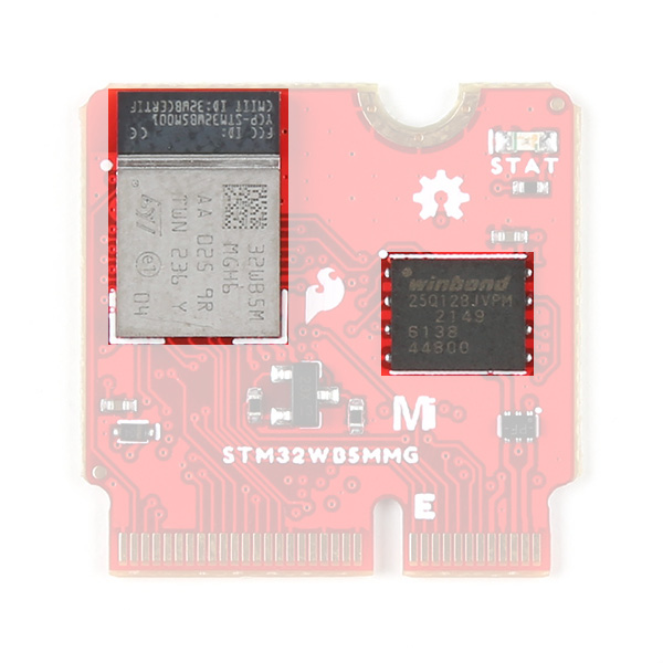
STM32WB5MMG Multiprotocol Wireless Module
The STM32WB5MMG module is an ultra-low power combination of two Arm-Cortex processors that provides a powerful computing platform with Bluetooth Low Energy 5.3 and 802.15.4 wireless capabilities. The module uses a Cortex-M4 CPU with FPU and ART for primary computing and a Cortex-M0 for the radio and security. For a complete overview of the module, refer to the STM32WB5MMG datasheet and application manual.
The STM32WB5MMG boasts a wide range of interface options and this Processor routes the following interfaces to the pinout on the M.2 connector:
- 2x UART (Standard and Low Power)
- 2x I2C
- SPI
- I2S[1]
- 16-bit Advanced Four-Channel Timer
The module features multiple low-power modes including a shutdown mode that consumes only 13 nA and draws 5.2 mA during radio transmission (Tx at 0 dBm). The module uses an integrated chip antenna for the RF stack with Tx output power up to +6 dBm and Rx sensitivity of -96 dBm for BLE and -100 dBm for 802.15.4 protocols.
W25Q128JVPIM Flash IC
This Processor includes a W25Q128JVPIM 128 Mbit (16 MB) Flash IC to provide extra storage functionality. The Flash IC connects to the STM32WB5MMG's QSPI interface.
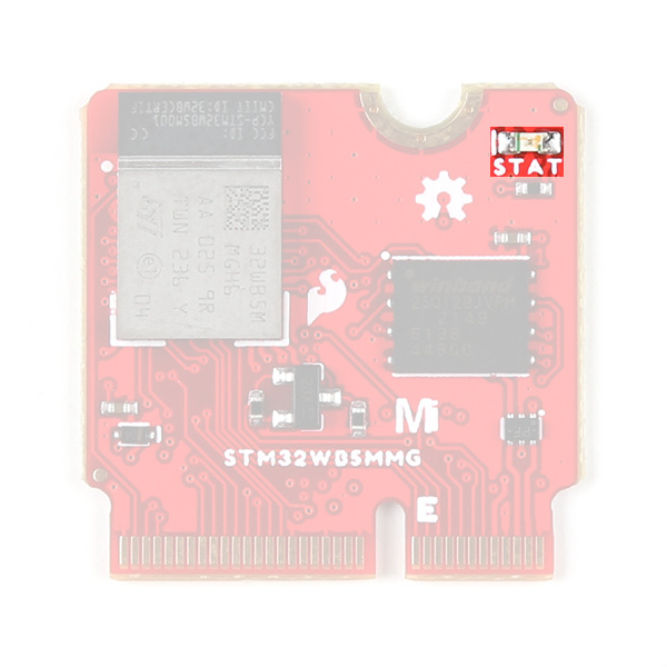
Status LED
The lone LED on this board is tied to the module's PA2 I/O pin to act as a status LED.
MicroMod Pinout
The table below outlines the pin map of this Processor Board as well as the general MicroMod pinout and pin descriptions. Refer to this or the schematic for the complete overview of the pin map.
| AUDIO | UART | GPIO/BUS | I2C | SDIO | SPI | Dedicated |
| STM32WB Pin | Primary Function | Bottom Pin |
Top Pin |
Primary Function | STM32WB Pin |
|---|---|---|---|---|---|
| - | (Not Connected) | 75 | GND | - | |
| - | 3.3V | 74 | 73 | G5 / BUS5 | PA0 |
| - | V_BATT | 72 | 71 | G6 / BUS6 | PH1 |
| - | - | 70 | 69 | G7 / BUS7 | PH0 |
| - | - | 68 | 67 | - | - |
| - | - | 66 | 65 | - | - |
| - | - | 64 | 63 | - | - |
| - | - | 62 | 61 | SPI_POCI (O) | PA6 |
| - | - | 60 | 59 | SPI_PICO (I) | PA7 |
| PB8 | AUD_MCLK | 58 | 57 | SPI_SCK (O) | PA5 |
| PB15 | AUD_I2S_OUT | 56 | 55 | SPI_CS | PA4 |
| PB5 | AUD_I2S_IN | 54 | 53 | I2C_SCL1 (I/O) | PB6 |
| PA4 | AUD_FSYNC | 52 | 51 | I2C_SDA1 (I/O) | PB7 |
| PB9 | AUD_BCLK | 50 | 49 | BATT_VIN / 3 (I - ADC) (0 to 3.3V) | COMP1_INM/PC4 |
| PE3 | G4 / BUS4 | 48 | 47 | PWM1 | PD15/TIM1_CH2 |
| PD8 | G3 / BUS3 | 46 | 45 | GND | - |
| PC13 | G2 / BUS2 | 44 | 43 | - | - |
| PC11 | G1 / BUS1 | 42 | 41 | - | - |
| PE4 | G0 / BUS0 | 40 | 39 | GND | - |
| PC3/LPTIM1_ETR | A1 | 38 | 37 | - | - |
| - | GND | 36 | 35 | - | - |
| PC2/LPTIM1_IN2 | A0 | 34 | 33 | GND | - |
| PD14/TIM1_CH1 | PWM0 | 32 | 31 | Module Key | - |
| - | Module Key | 30 | 29 | Module Key | - |
| - | Module Key | 28 | 27 | Module Key | - |
| - | Module Key | 26 | 25 | Module Key | - |
| - | Module Key | 24 | 23 | SWDIO | PA13 |
| PC1/LPUART1_RX | TX2 (O) | 22 | 21 | SWDCK | PA14 |
| PC0/LPUART1_TX | RX2 (I) | 20 | 19 | RX1 (I) | PA10/DEV_TX1 |
| PE0/TIM1_ETR | D1/TIM1_ETR | 18 | 17 | TX1 (0) | PA9/DEV_RX1 |
| PA1 | I2C_INT | 16 | 15 | CTS1 | PB4 |
| PB6 | I2C_SCL (I/0) | 14 | 13 | RTS1 | PB3 |
| PB7 | I2C_SDA (I/0) | 12 | 11 | BOOT# (I - Open Drain) | BOOT0/PH3 |
| PB12 | D0/TIM1_BKIN | 10 | 9 | - | - |
| - | - | 8 | 7 | GND | - |
| - | RESET# (I - Open Drain) | 6 | 5 | USB_D- | PA11/USB_DM |
| - | - | 4 | 3 | USB_D+ | PA12/USB_DP |
| - | 3.3V | 2 | 1 | GND | - |
| Function | Bottom Pin |
Top Pin |
Function | ||||||
|---|---|---|---|---|---|---|---|---|---|
| (Not Connected) | 75 | GND | |||||||
| 3.3V | 74 | 73 | G5 / BUS5 | ||||||
| RTC_3V_BATT | 72 | 71 | G6 / BUS6 | ||||||
| SPI_CS1# | SDIO_DATA3 (I/O) | 70 | 69 | G7 / BUS7 | |||||
| SDIO_DATA2 (I/O) | 68 | 67 | G8 | ||||||
| SDIO_DATA1 (I/O) | 66 | 65 | G9 | ADC_D- | CAM_HSYNC | ||||
| SPI_PICO1 | SDIO_DATA0 (I/O) | 64 | 63 | G10 | ADC_D+ | CAM_VSYNC | |||
| SPI POCI1 | SDIO_CMD (I/O) | 62 | 61 | SPI_PICO (I) | |||||
| SPI SCK1 | SDIO_SCK (O) | 60 | 59 | SPI_POCI (O) | LED_DAT | ||||
| AUD_MCLK (O) | 58 | 57 | SPI_SCK (O) | LED_CLK | |||||
| CAM_MCLK | PCM_OUT | I2S_OUT | AUD_OUT | 56 | 55 | SPI_CS# | |||
| CAM_PCLK | PCM_IN | I2S_IN | AUD_IN | 54 | 53 | I2C_SCL1 (I/O) | |||
| PDM_DATA | PCM_SYNC | I2S_WS | AUD_LRCLK | 52 | 51 | I2C_SDA1 (I/O) | |||
| PDM_CLK | PCM_CLK | I2S_SCK | AUD_BCLK | 50 | 49 | BATT_VIN / 3 (I - ADC) (0 to 3.3V) | |||
| G4 / BUS4 | 48 | 47 | PWM1 | ||||||
| G3 / BUS3 | 46 | 45 | GND | ||||||
| G2 / BUS2 | 44 | 43 | CAN_TX | ||||||
| G1 / BUS1 | 42 | 41 | CAN_RX | ||||||
| G0 / BUS0 | 40 | 39 | GND | ||||||
| A1 | 38 | 37 | USBHOST_D- | ||||||
| GND | 36 | 35 | USBHOST_D+ | ||||||
| A0 | 34 | 33 | GND | ||||||
| PWM0 | 32 | 31 | Module Key | ||||||
| Module Key | 30 | 29 | Module Key | ||||||
| Module Key | 28 | 27 | Module Key | ||||||
| Module Key | 26 | 25 | Module Key | ||||||
| Module Key | 24 | 23 | SWDIO | ||||||
| UART_TX2 (O) | 22 | 21 | SWDCK | ||||||
| UART_RX2 (I) | 20 | 19 | UART_RX1 (I) | ||||||
| CAM_TRIG | D1 | 18 | 17 | UART_TX1 (0) | |||||
| I2C_INT# | 16 | 15 | UART_CTS1 (I) | ||||||
| I2C_SCL (I/0) | 14 | 13 | UART_RTS1 (O) | ||||||
| I2C_SDA (I/0) | 12 | 11 | BOOT (I - Open Drain) | ||||||
| D0 | 10 | 9 | USB_VIN | ||||||
| SWO | G11 | 8 | 7 | GND | |||||
| RESET# (I - Open Drain) | 6 | 5 | USB_D- | ||||||
| 3.3V_EN | 4 | 3 | USB_D+ | ||||||
| 3.3V | 2 | 1 | GND | ||||||
| Signal Group | Signal | I/O | Description | Voltage | Power | 3.3V | I | 3.3V Source | 3.3V |
|---|---|---|---|---|
| GND | Return current path | 0V | ||
| USB_VIN | I | USB VIN compliant to USB 2.0 specification. Connect to pins on processor board that require 5V for USB functionality | 4.8-5.2V | |
| RTC_3V_BATT | I | 3V provided by external coin cell or mini battery. Max draw=100μA. Connect to pins maintaining an RTC during power loss. Can be left NC. | 3V | |
| 3.3V_EN | O | Controls the carrier board's main voltage regulator. Voltage above 1V will enable 3.3V power path. | 3.3V | |
| BATT_VIN/3 | I | Carrier board raw voltage over 3. 1/3 resistor divider is implemented on carrier board. Amplify the analog signal as needed for full 0-3.3V range | 3.3V | |
| Reset | Reset | I | Input to processor. Open drain with pullup on processor board. Pulling low resets processor. | 3.3V |
| Boot | I | Input to processor. Open drain with pullup on processor board. Pulling low puts processor into special boot mode. Can be left NC. | 3.3V | |
| USB | USB_D± | I/O | USB Data ±. Differential serial data interface compliant to USB 2.0 specification. If UART is required for programming, USB± must be routed to a USB-to-serial conversion IC on the processor board. | |
| USB Host | USBHOST_D± | I/O | For processors that support USB Host Mode. USB Data±. Differential serial data interface compliant to USB 2.0 specification. Can be left NC. | |
| CAN | CAN_RX | I | CAN Bus receive data. | 3.3V |
| CAN_TX | O | CAN Bus transmit data. | 3.3V | |
| UART | UART_RX1 | I | UART receive data. | 3.3V |
| UART_TX1 | O | UART transmit data. | 3.3V | |
| UART_RTS1 | O | UART ready to send. | 3.3V | |
| UART_CTS1 | I | UART clear to send. | 3.3V | |
| UART_RX2 | I | 2nd UART receive data. | 3.3V | |
| UART_TX2 | O | 2nd UART transmit data. | 3.3V | |
| I2C | I2C_SCL | I/O | I2C clock. Open drain with pullup on carrier board. | 3.3V |
| I2C_SDA | I/O | I2C data. Open drain with pullup on carrier board | 3.3V | |
| I2C_INT# | I | Interrupt notification from carrier board to processor. Open drain with pullup on carrier board. Active LOW | 3.3V | |
| I2C_SCL1 | I/O | 2nd I2C clock. Open drain with pullup on carrier board. | 3.3V | |
| I2C_SDA1 | I/O | 2nd I2C data. Open drain with pullup on carrier board. | 3.3V | |
| SPI | SPI_POCI | O | SPI Controller Output/Peripheral Input. | 3.3V |
| SPI_PICO | I | SPI Controller Input/Peripheral Output. | 3.3V | |
| SPI_SCK | O | SPI Clock. | 3.3V | |
| SPI_CS# | O | SPI Chip Select. Active LOW. Can be routed to GPIO if hardware CS is unused. | 3.3V | |
| SPI/SDIO | SPI_SCK1/SDIO_CLK | O | 2nd SPI Clock. Secondary use is SDIO Clock. | 3.3V |
| SPI_POCI1/SDIO_CMD | I/O | 2nd SPI Controller Output/Peripheral Input. Secondary use is SDIO command interface. | 3.3V | |
| SPI_PICO1/SDIO_DATA0 | I/O | 2nd SPI Peripheral Input/Controller Output. Secondary use is SDIO data exchange bit 0. | 3.3V | |
| SDIO_DATA1 | I/O | SDIO data exchange bit 1. | 3.3V | |
| SDIO_DATA2 | I/O | SDIO data exchange bit 2. | 3.3V | |
| SPI_CS1/SDIO_DATA3 | I/O | 2nd SPI Chip Select. Secondary use is SDIO data exchange bit 3. | 3.3V | |
| Audio | AUD_MCLK | O | Audio master clock. | 3.3V |
| AUD_OUT/PCM_OUT/I2S_OUT/CAM_MCLK | O | Audio data output. PCM synchronous data output. I2S serial data out. Camera master clock. | 3.3V | |
| AUD_IN/PCM_IN/I2S_IN/CAM_PCLK | I | Audio data input. PCM syncrhonous data input. I2S serial data in. Camera periphperal clock. | 3.3V | |
| AUD_LRCLK/PCM_SYNC/I2S_WS/PDM_DATA | I/O | Audio left/right clock. PCM syncrhonous data SYNC. I2S word select. PDM data. | 3.3V | |
| AUD_BCLK/PCM_CLK/I2S_CLK/PDM_CLK | O | Audio bit clock. PCM clock. I2S continuous serial clock. PDM clock. | 3.3V | |
| SWD | SWDIO | I/O | Serial Wire Debug I/O. Connect if processor board supports SWD. Can be left NC. | 3.3V |
| SWDCK | I | Serial Wire Debug clock. Connect if processor board supports SWD. Can be left NC. | 3.3V | |
| ADC | A0 | I | Analog to digital converter 0. Amplify the analog signal as needed to enable full 0-3.3V range. | 3.3V |
| A1 | I | Analog to digital converter 1. Amplify the analog signal as needed to enable full 0-3.3V range. | 3.3V | |
| PWM | PWM0 | O | Pulse width modulated output 0. | 3.3V |
| PWM1 | O | Pulse width modulated output 1. | 3.3V | |
| Digital | D0 | I/O | General digital input/output pin. | 3.3V |
| D1/CAM_TRIG | I/O | General digital input/output pin. Camera trigger. | 3.3V | |
| General/Bus | G0/BUS0 | I/O | General purpose pins. Any unused processor pins should be assigned to Gx with ADC + PWM capable pins given priority (0, 1, 2, etc.) positions. The intent is to guarantee PWM, ADC and Digital Pin functionality on respective ADC/PWM/Digital pins. Gx pins do not guarantee ADC/PWM function. Alternative use is pins can support a fast read/write 8-bit or 4-bit wide bus. | 3.3V |
| G1/BUS1 | I/O | 3.3V | ||
| G2/BUS2 | I/O | 3.3V | ||
| G3/BUS3 | I/O | 3.3V | ||
| G4/BUS4 | I/O | 3.3V | ||
| G5/BUS5 | I/O | 3.3V | ||
| G6/BUS6 | I/O | 3.3V | ||
| G7/BUS7 | I/O | 3.3V | ||
| G8 | I/O | General purpose pin | 3.3V | |
| G9/ADC_D-/CAM_HSYNC | I/O | Differential ADC input if available. Camera horizontal sync. | 3.3V | |
| G10/ADC_D+/CAM_VSYNC | I/O | Differential ADC input if available. Camera vertical sync. | 3.3V | |
| G11/SWO | I/O | General purpose pin. Serial Wire Output | 3.3V |
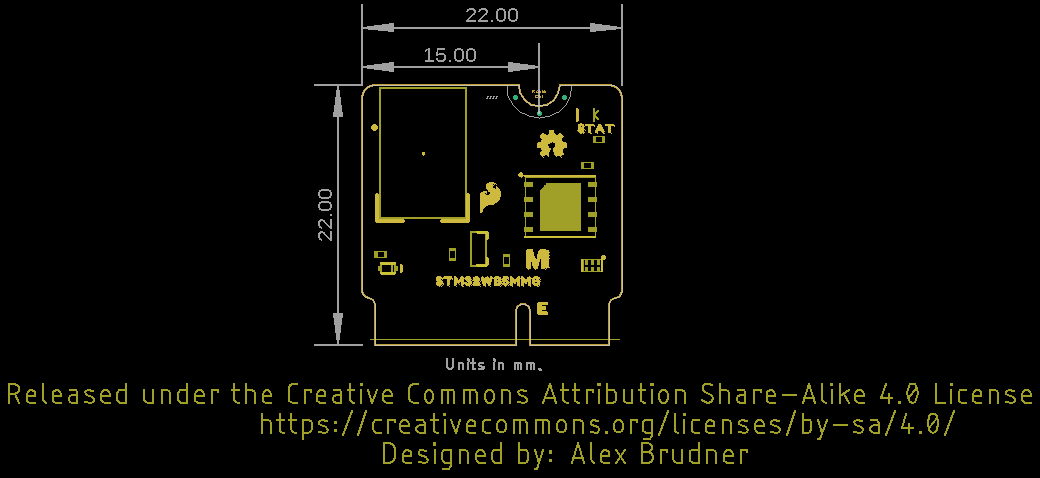
Board Dimensions
This Processor matches the MicroMod Processor standard sizing and measures 22mm x 22mm, with 15mm to the top notch and 12mm to the E key. For more information regarding the processor board physical standards, head on over to the Getting Started with MicroMod and Designing With MicroMod tutorials.