LSM6DS3 Breakout Hookup Guide
 MTaylor
Hardware Overview
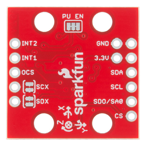
The Pinout
In total, the LSM9DS0 Breakout breaks out 11 pins.
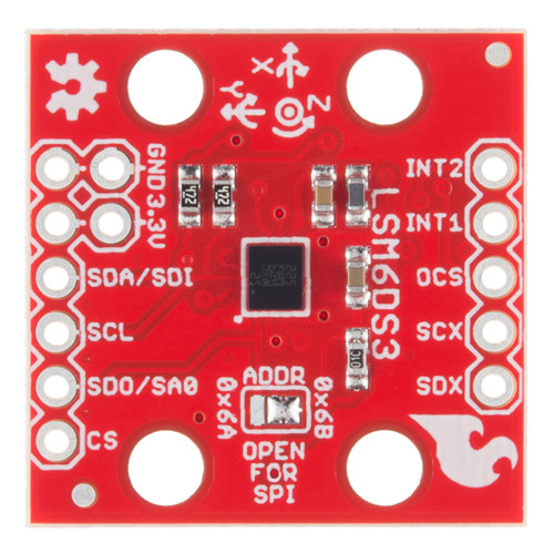
The bare-minimum connections required are broken out on the left side of the board. These are the power and I2C pins (the communication interface the board defaults to). These pins can be used for the SPI interface as well:
| Pin Label | Pin Function | Notes |
|---|---|---|
| GND | Ground | 0V voltage supply. Spare GND pin to connect more stuff! |
| VDD | Power Supply | Supply voltage to the chip. Should be regulated between 1.8V and 3.6V. Spare VDD provided for general use as well. |
| SDA/SDI | I2C: Serial Data SPI: MOSI | I2C: Serial data (bi-directional) SPI: Device data in (MOSI) |
| SCL | Serial Clock | I2C and SPI serial clock. |
| SDO/SA0 | I2C: Address SPI: MISO | I2C: Address LSB SPI: Device data out (MISO) |
| CS | I2C: Mode SPI: CS | I2C: Select I2C (disconnected) SPI: Chip select (Slave select) |
The remaining pins are broken out on the other side. These pins break out SPI functionality and interrupt outputs:
| Pin Label | Pin Function | Notes |
|---|---|---|
| INT2 | Accel/Gyro Interrupt 2 | INT1 and INT2 are programmable interrupts for the accelerometer and gyroscope. They can be set to alert on over/under thresholds, data ready, or FIFO overruns. Make sure these are connected to an INPUT pin to prevent driving 5v back into the LSM6DS3. |
| INT1 | Accel/Gyro Interrupt 1 | |
| OCS | Aux SPI 3-wire | These pins are used to attach slave I2C and 3-wire devices for FIFO data collection. This function is not covered in this tutorial. |
| SCX | Aux Clock | |
| SDX | Aux Data |
Power Supply
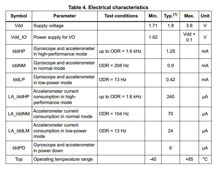
The VDD and GND pins are where you'll supply a voltage and 0V reference to the IC. The breakout board does not regulate this voltage, so make sure it falls within the allowed supply voltage range of the LSM9DS0: 1.8V to 3.6V. Below is the electrical characteristics table from the datasheet.
The communication pins are not 5V tolerant, so they'll need to be regulated to within a few mV of VDD.
Interrupts
There are a variety of interrupts on the LSM6DS3. While connecting these is not as critical as the communication or power supply pins, using them will help you get the most out of the chip.
The interrupt pins are INT1 and INT2. One or both pins can be software configured and mapped to the following conditions:
- Step detected
- Step detected after delta time
- Step counter overflowed
- Significant motion (shock, drop)
- FIFO full
- FIFO overrun
- FIFO threshold reached (Datasheet calls this the "watermark"
- Boot status
- Gyroscope data ready
- Accelerometer data ready
- Inactivity
- Single tap
- Wake-up
- Free-fall
- Double tap
- 6D (orientation)
- Tilt
- Timer
- Wake-up
- Ironing interrupt
Only a few interrupt examples are provided. See the datasheet and application guide for using the advanced interrupt features.
The Jumpers
| Jumper Label | Jumper Function |
|---|---|
| ADDR | Use to sellect address 0x6A or 0x6B(default) for I2C communication. This jumper must be opened for SPI mode, or the MISO line will not supply data |
| PU_EN | This trace-connected jumper enables 4.7k resistors on SDA and SCL for I2C. SPI works with these connected, but really they should be cut apart for better signal shape at high speeds and to lower power consumption |
| SCX and SDX | ST recommends pulling the unused SCX and SDX to power or ground when not in use. If connecting slave devices, cut these traces. |
The ADDR jumper is commonly reconfigured for I2C addresses and SPI mode, so it is solder jumpered.
The other jumpers are probably not for most users, but if it is necessary, whip out your handy hobby knife, and carefully cut the small traces between pads. Even if you're using SPI, though, the jumpers shouldn't hinder your ability to communicate with the chip.