Designing PCBs: SMD Footprints
Getting Started
If you’re eagerly reading this tutorial you’re getting pretty deep into the plumbing of Eagle. Congratulations! Keep going!
We’re going to assume you’ve already read our other tutorials on through-hole and SMD PCB layout so you should already have Eagle and the various support files installed. We use keyboard shortcuts liberally so you better have them installed as well.
This tutorial will show you how to create a custom SMD footprint and schematic symbol library. This is a crucial skill for any hacker who wants access to the latest technology via SMD modules or new SMD ICs.
Suggested Reading
Here are some concepts that this tutorial builds upon and that you may need to know:
Choosing a Part
As new ICs come out, the PCB layout softwares of the world will not have that specific part within their component libraries. For example, Eagle may have a given footprint (SOIC-8 or QFN-24) but I wouldn’t trust it. I have lost so much money on PCBs that had the wrong footprint that I don’t use the built-in libraries, Eagle or other. Sometimes I’ll use a friend’s library, but we all make mistakes (I actually owe David Mellis a beer for messing up one of his boards because he relied on a footprint of ours). Don’t trust anyone or anyone’s library without a one-to-one print and a thorough review of the datasheet and pin mapping.
The FT230X from FTDI looks like an interesting new IC. Let’s do a breakout board for it. Before we can start laying out a board, we’ll need to create a brand new footprint (aka 'package' in Eagle), schematic symbol, and device for it before we can begin to layout a PCB.
In other words:
or using Eagle's language
Now that we've chosen a part, let's make a footprint for it!
Footprint Creation
Eagle requires three things to get an IC into the library:
- Package (also known as a footprint)
- Symbol (the schematic symbol)
- Device (mapping them together)
The tutorial images show us working from the SparkFun-DigitalIC.lbr file but you can create your own custom library file if you'd like.
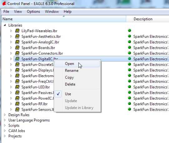
We are going to start by creating a footprint from scratch. Because the FT230X is a digital IC, let’s open the SparkFun-DigitalIC library.
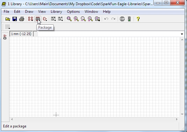
We’ve got a clean slate! Click on ‘package’
Now bring up the datasheet for the FT230X and skim down to where the package is described. This IC uses a package type called SSOP16 and has 16 pins. Wikipedia has some good information about SSOP (Shrink small-outline package) chips. For our purposes, we need only to get a short package identifier into Eagle.
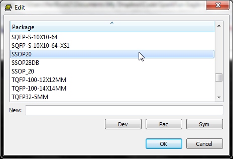
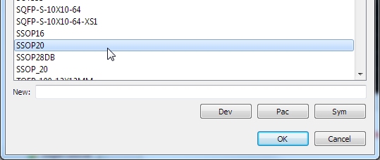
From within the Eagle footprint list, click on any footprint in this window and press ‘s’. This will bring you to the packages starting with the letter S. Now is your chance to see if the package you are about to create is already available. In our case, ‘SSOP20’ is available but SSOP16 (the 16 derivative) is not.
To create a new package, type the name SSOP16 into the 'New:' box. This fits with the same naming structure as the SSOP20 package.
Do you already have a SSOP16 in your library? (Look at you, you have the most up to date library!) Go ahead and call this one ‘SSOP16-PRACTICE’ or some such name that you can find later.
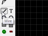
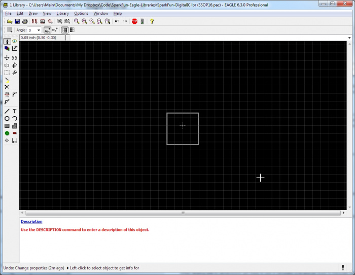
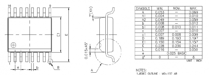
Now we’ve got a black window of nothing. From the datasheet, this IC is E1 (0.154”) wide and D (0.193”) long. For now, let’s create a square on the tDocu (top document) layer. Click on ‘Wire’.
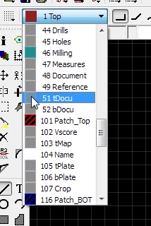
We can now draw, but we need to get to the tDocu layer. To do this you can either drop down the layers menu and select layer 51 tDocu or...
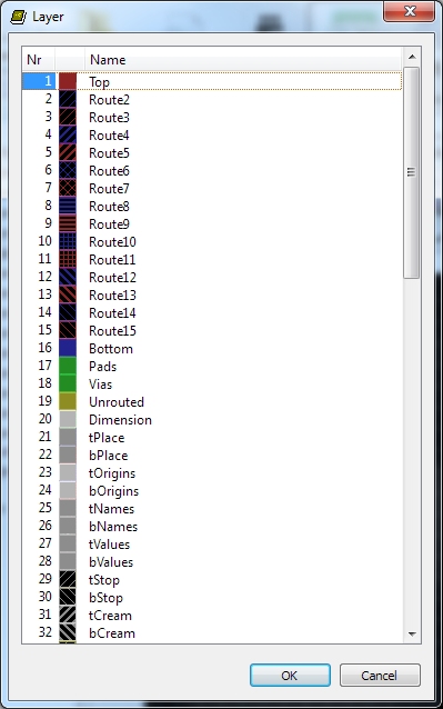
click the center button/scroll wheel on your mouse. I much prefer using the scroll wheel to select the layer because I jump to different layers a lot. You’ll see a ton of different layers. Find layer 51 and click it.
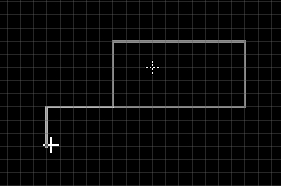
Draw a box. Hit escape to stop drawing. This is not really the shape of the IC. To get the exact shape, let’s look at the dimensions of the IC again. 0.154” wide and 0.193” long. Every manufacturer will have different tolerances. Use the nominal (NOM) dimension when it is provided. If you only have MIN and MAX dimensions, I will use the usually take the midpoint between them.
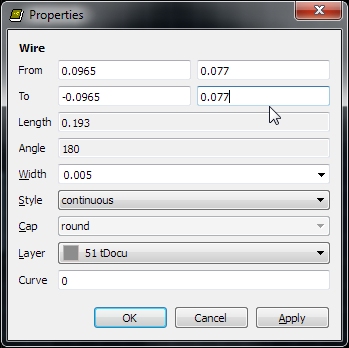
In Eagle, we want the component to have 0,0 centrally located within the component. So if the X dimension is 0.193 the left side of the box will be -0.0965, right side will be 0.0965. Let’s modify the left and right sides to be at these X locations.
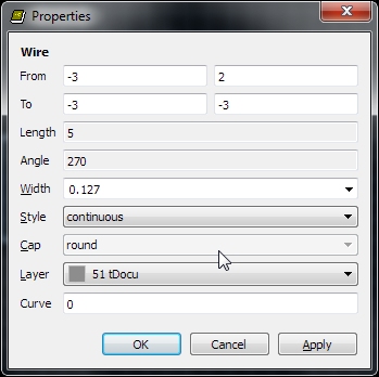
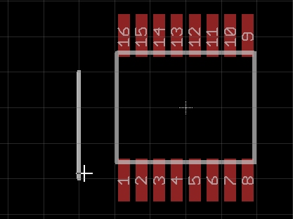
Click the ‘i’ button and then select the left gray bar by left clicking on it. We are now modifying the X and Y coordinates of the starting and ending points of this line. Note that in this picture by line is -3,2 to -3,-3. I’m on the wrong grid! I’m on the metric grid but our dimensions are in imperial. This is a common problem and you will be jumping between grid types often.
To switch between grid types, exit out of any window, then hit F10 for the standard imperial grid and Alt+F10 for the metric grid.
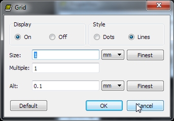
To change the grid to something really wild, click on the Grid button in the upper left corner of the menu bar. Here you can modify many different settings. In general, we stick to:
- 0.05inch size with 0.005inch alternative size for the imperial grid
- 1mm size with 0.1mm alternative size for the metric grid
Again, learn the F10 and Alt+F10 shortcuts. They will save you lots of time.
Close this window and hit F10 to change to the imperial grid. Now click on the ‘i’, then left click on the left bar of the box we drew.
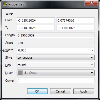
Our lengths look really weird because this line was drawn in metric and is being converted to inch. Let’s modify this to -0.0965".
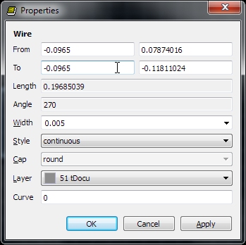
Repeat for the right bar with 0.0965”.
Whoa. This IC is getting smaller!
Now let’s modify the top bar and bottom bar to be 0.154" / 2 = 0.077"
Ahh! We now have the physical outline of this SSOP package. It’s small!
Time to save your work. Click on the disk icon or hit Ctrl+s.
When dealing with IC dimensions have a calculator handy and be ready to convert between metric and imperial (I’m lazy and use google). If you don’t have a datasheet for your part, don’t fret! Get the part in your hand, pull out your digital calipers and start measuring. We've created many parts without a datasheet.
Now we need to add SMD pads around this outline. From the datasheet, each pad is:
- 0.041” long : (dimension E - dimension E1) / 2
- 0.01” wide : dimension b
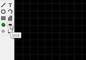
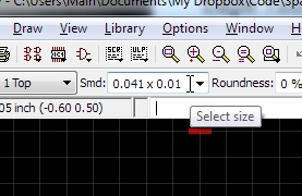
Click on Smd (come on Eagle! It’s SMD not Smd!). You’ll have a red rectangle floating around. Now go up to the Smd: box and enter 0.041x0.01.
Now wait! We have created a pad that is exactly the size of the pin. We actually want a pad that is slightly longer and slightly wider than the pin so that we can have solder fill around the pin and the pad. I will sometimes increase by ~10-20% in each direction. There is no hard and fast rule here. We often find recommended footprint datasheets for similar footprints. For this example, I’m going to look at the SSOP20 footprint contained within the Digital ICs library and use the pad dimensions for that component. I know SSOP20 works well (we've used the old FT232 IC many times) so I trust that pad size.
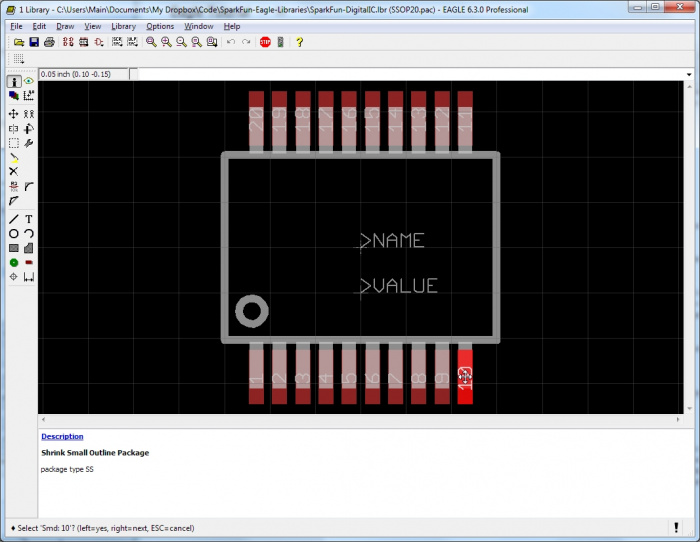
Click on the Package button in the top menu within the Eagle window then scroll to SSOP20.
Click on the ‘i’ (not the eye ball) and click on a pad. Make sure the red pad is highlighted and not the white pad. If the wrong pad is highlighted, right click and Eagle will cycle through the items that are stacked upon each other.
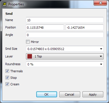
0.01574803 x 0.05905512 ?!? What the heck is that? Remember, we are on the imperial grid. Let’s close this window and hit Alt+F10 to switch to the metric grid. You should see the grid change in size. Now click on the same pad. If the white block gets highlighted hit escape (to close the pad information window) and trying clicking on the more central location of the red pad.
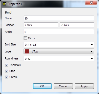
0.4 x 1.5 - Ahah! This makes a lot more sense. The pad was created on the metric grid. Let’s do the same for our component. Remember this value.
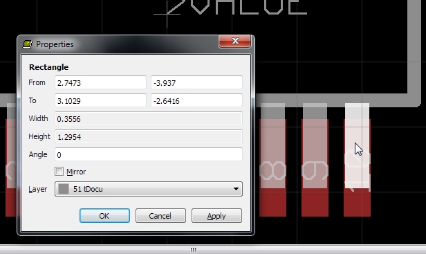
Before we leave this package, let’s talk about the tDocu layer and why there is a white square on top of the red square. Remember how we said we needed to create a pad that is bigger than the pin? The person who created this package created a white square to indicate the actual pin on the top document layer (tDocu) and an actual electrical pad using the Smd button. This allows the engineer to see where exactly the pin is located and where the SMD pad is located underneath. This white pad is really just there to help us visualize everything going on. Also note that the red pad is not concentric (does not share the same center point) as the white square.
(picture of pin on pad at angle)
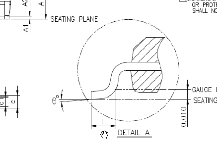
This is because only part of the pin hits the pad. This is dimension L on the datasheet:
This is all pretty minute details to creating the pad for this device. For your own SMD package remember:
- Create a SMD pad that is slightly larger than the pin dimensions
- Locate the pad so that it is near the center of where the metal pin will be
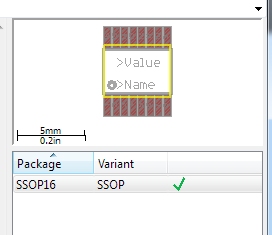
Ok - now let’s return to the new SSOP16 footprint we were creating. Click on the ‘Package’ button located in the top Eagle menu, scroll down to the SSOP16 package and double click it. You should now see the white box we created.
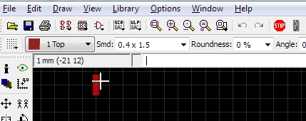
Click on SMD and create a pad that is 0.4x1.5.
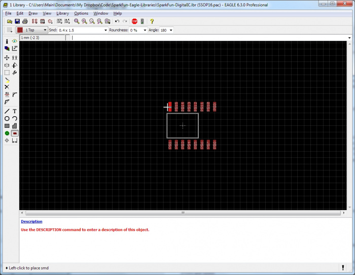
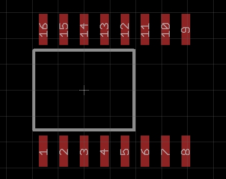
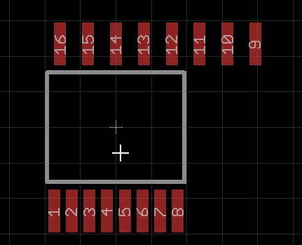
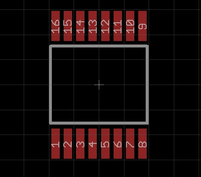
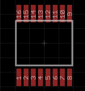
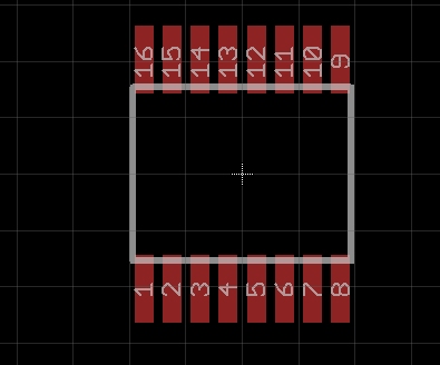
Drop 16 pads (this is a 16-pin device) around the outline of the package.
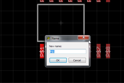
Let's rename the pads to ‘1’, ‘2’, etc as they are labeled in the datasheet (the pin numbers wrap around the device in a counter clockwise fashion).
Press F4 to go into Name mode (or click on the Name button). Then click on the lower left pad. Rename this pad to ‘1’. Goto the next pad and name it 2, and so on.
All done. You might be thinking that you should be naming the pads for what they actually do (1 is TX, 2 is RTS#, etc). This is incorrect. We are making a generic SSOP16 package. Later we will associate the pin function with pad #s. For now, just be sure you are number the pins correctly. Connectors are often numbered differently from ICs so read your datasheet closely.
Back on the datasheet, look at the e dimension (little e, not big E). This is the distance between pins, also known as pin pitch. For this IC, the pitch is 0.025”.
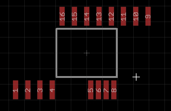
There are 8 pins on each side so I am going to start on the lower row of pads, setting pad 5 at +0.0125” (1/2 of 0.025”). Click on the ‘i’ button, then on Pad 5. Adjust the X location to 0.0125 then click ok.
Pad 6 will be at 0.0125 + 0.025 = 0.0375”. Pad 7 will be at 0.0625, etc. Repeat for pads 5 through 8.
Neat! Those pads are pretty close together but it looks like the spacing is making sense.
Now do the same for pads 1 to 4. Pad 4 will be ½ of 0.025 = -0.0125”. Pad 3 will be -0.0125 - 0.025 = -0.0375 and so on.
You should now have the bottom pads with the correct X coordinates. Now, leveraging symmetry, we can use those same X coordinates and do pads 9 to 16. Click on each pad (I started with 16 and worked my way right) and adjust the X coordinate.
Now we need to calculate and adjust the Y coordinate for all pads. This is a bit tricky, but get the datasheet in front of you and follow along:
We want the SMD pad to be located under the center of pin (metal leg) of the device. We want to find the dimension from the center of the IC to the center of the metal leg. We can infer this from dimension E (0.236”) and dimension L ( MAX 0.05 - MIN 0.016 / 2 = 0.033”).
From the center of the IC to the outside edge of a metal leg is E/2 (0.236 / 2 = 0.118”).
Then we need to come back ½ the width of the metal leg which is L / 2 (0.033 / 2 = 0.0165”).
So 0.118 - 0.0165 = 0.1015”. It is 0.1015" from the center of the part to the middle of each metal leg.
This is the Y coordinate for all the pads on the top row (16 to 9). Let’s adjust them by clicking on ‘i’ then on each pad, correcting the Y coordinate to 0.1015” as we go.
The top row has been adjusted. This looks pretty good. Let’s bring the bottom row up as well.
Time to save your work! Hit the disk icon or hit Ctrl+s.
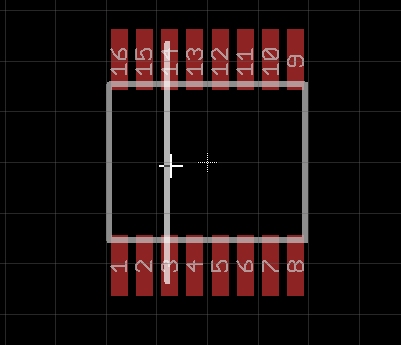
Now let’s check our work. We know the outer dimension of the legs is E (0.236”), so let’s draw a line on tDocu. Click on the ‘wire’ button and draw a line that is a few grids long:
Hit escape to stop drawing. Now modify the Y coordinate of this line (by hitting ‘i’ and clicking on the line) to be 0.118 to -0.118. This line now represents the exterior edge of the pins on the actual IC. Press F7 to go into ‘move’ mode. Then click on the line you just created. Now you should be able to move this line around.
The line will jump around on the major grid. To go to the alternate grid, press and hold the ‘alt’ key as you move the mouse. The line should move with much more fine adjustment now.
We’re using the line as a measuring stick to see where the edges of the pins will fall on the pads. Does it look like the edge of the pins will fall towards the middle of the pads? Yep. Looks pretty good to me. Move the line somewhere off to the side and click once to drop it there. Now hit F3 to go in to ‘delete’ mode and click the line to delete it.
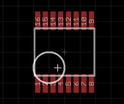
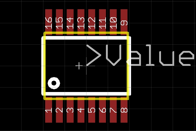
Let’s add a pin 1 indicator by clicking the 'circle' button. The last time we drew anything it was on the tDocu layer. We want this indicator to appear in the silkscreen on the PCB so that we know how to orient the IC on our board. So before we start drawing, click the scroll wheel of your mouse to bring up the layers window and select tPlace (top placement is the silkscreen layer on the PCB).
Now move your cursor in the bottom left corner near pin 1 and click once. What the?! Eagle is trying to snap to the major grid. That’s bad. Hit escape to cancel this drawing. You should still be in circle mode. Hold the alt button, move your cursor where you want the center of the circle and click once then move your mouse cursor.
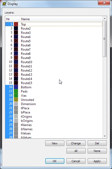
Ahah! The circle is now where we roughly want it. Notice that the tPlace layer (which will get printed) looks identical in color to the tDocu layer (which is only used for reference and will not get printed on the PCB). Confusing! So let’s fix this by modifying the layer colors. Click on the ‘display’ button located on the left menu bar under the 'i' button.
Here we see a multitude of layers. I am going to delete layers Route2 through Route15 because I have never created a footprint that had interior layers. You may want to leave them if you’re a super user.
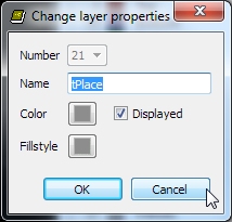
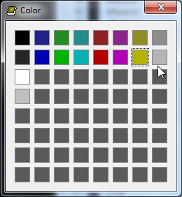
Double click on tPlace. Then click on the gray square next to Color. Change the color to white. Click on ok to back out to the layers window.
Now let’s change the color for tDocu. Change it to mellow yellow.
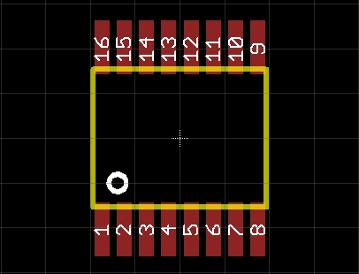
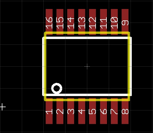
Ahh! That’s a bit easier to visualize what’s going on. White will be silkscreened. Yellow is just there so we know where the IC edges are. I prefer to have a white box one my PCB indicating where an IC goes so let’s draw some lines on the tPlace layer.
Here I’ve made a white box, slightly longer than the tDocu lines and slightly skinnier. This will prevent me from putting anything too close to the end of my IC, possibly hitting a nearby component. However, there is a problem with this. Silkscreen should have a thickness of 0.008” or larger so that the PCB fab house can print it legibly. Trying to print too small of silkscreen will cause line to flake off and turn text into white blobs.
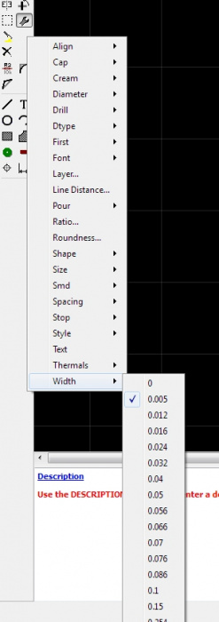
So let’s modify this silkscreen width to be 0.008” by clicking on the ‘Change’ wrench, then ‘Width’ then the ‘...’ at the very end of the list. You’ll get a window where you can enter your own width. Enter ‘0.008’ and press enter. Any line you click on will now change to 0.008”
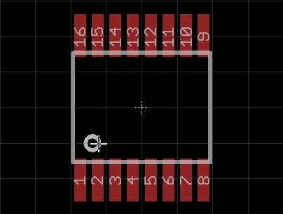
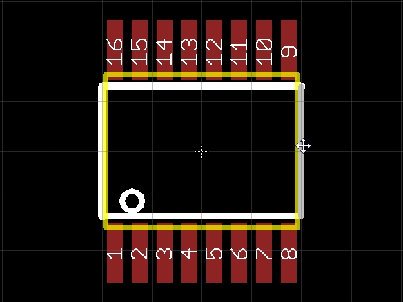
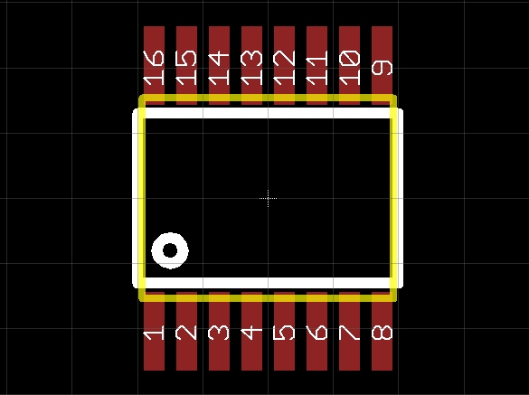
Click on each white line increasing its thickness. Also click on the pin 1 indicator circle. The circle is now kind of close to the edge so let’s move that up and over a bit. Do so by hitting F7 to go into move mode. Click on the middle of the circle. It will want to snap to the major grid so hold alt down while you move the circle and it will give you more fine placement.
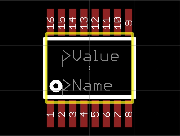
The final thing to do is add a ‘>Value’ and ‘>Name’ text tags on the tValues and tNames layers respectively. Eagle looks for these special tags and populates them with the value and name of the IC when you’re in PCB layout mode. Eventually, we will see ‘FT230X’ and ‘U3’ automatically populated here.
Click the ‘text’ button. Eagle will prompt you for the text. Type >Value and press enter. Before placing the text, click your scroll wheel and select the tValues layer.
As you move around, you'll see that this text is a bit large so I am going to change the size to 0.025. Find the Size box in the top menu bar. Type 0.025 and press enter.
Now place the text in the middle of the IC by holding the alt button (to get finer grid). Once you’re happy, left click once to place the text. Hit escape. You’ll be returned to the ‘Enter text’ window. Hit escape a second time to return to the main window. Now repeat the process but this time with >Name and place it on the tNames layer.
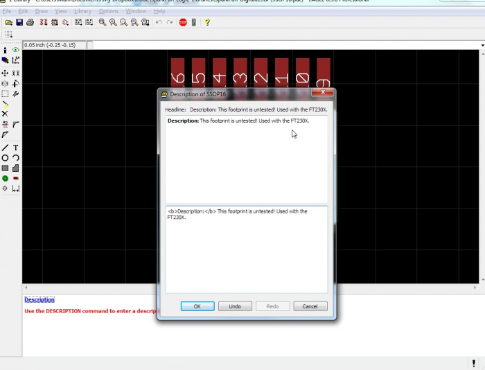
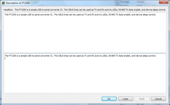
Looking really good! Be sure to give some sort of description to your package. Do this by clicking on the blue ‘Description’ line at the bottom of your screen. Eagle will bring up a window that allows you to edit this package’s description.
I like to put information about what component this package goes with. In our case, we’re creating this package for the FT230X but it could be used for other SSOP16 sized ICs. I also like to mention when this is a new/untested footprint or when it has been fully tested. The problem with this is that I often forget to come back and update the package description so do what you wish. Save your work!
Congratulations! You’re done with creating the SSOP16 package! Now let’s create the schematic symbol.
Symbol Creation
Eagle requires three things to get an IC into the library:
- Package (also known as a footprint)
- Symbol (the schematic symbol)
- Device (mapping them together)
The tutorial images show us working from the SparkFun-DigitalIC.lbr file but you can create your own custom library file if you'd like.
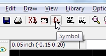
It's time to create the schematic symbol. Click on the ‘symbol’ button.
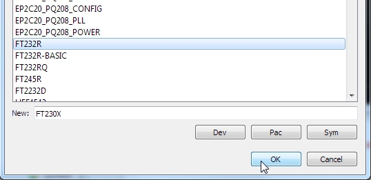
Now give this symbol a name. We are creating the schematic component for the FT230X, and we see that we don’t have another symbol with that name, so let’suse it!
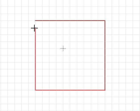
Start by clicking on 'Wire' and drawing a square box. Press escape to stop drawing.
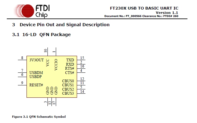
Now how many functional pins does the FT230X have? I ask about ‘functional’ pins because some ICs have pins that are not labeled or labeled as NC (Not Connected). I generally don’t show NC pins on my schematic symbols as they can clutter things up. In the case of the FT230X, all 16 pins have a function.
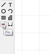
You’ll find the ‘pin’ button on the left menu. Click it.
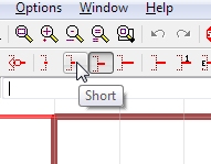
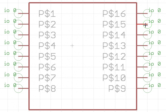
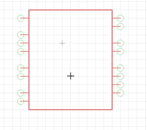
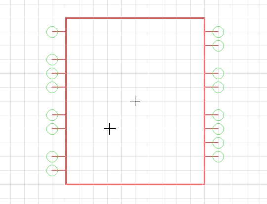
Once you’ve are in ‘pin’ mode you’ll get a different menu at the top of the screen. Click on ‘short’ to shorten the length of this pin indicator. I do this to save space. Now place 16 pins around the box.
Time to save your work! Hit the disk or Ctrl+s.
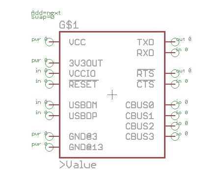
That is one ugly schematic symbol. Now let’s name each pin. Press F4 to go into naming mode and then click on the first pin P$1.
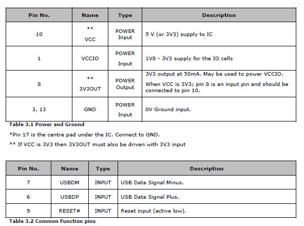
I am going to start at the top of the list with VCC and work my way down the datasheet list so that I don’t miss any. Note that there are two GND pins (3 and 13) so make two pins with that name.
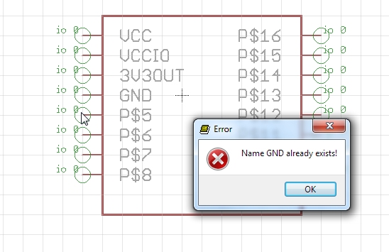
Oh no! You cannot name two pins with the same name. To get around this Eagle allows you to name pins with the @ sign. So name the first GND pin GND@3 (meaning GND pin at pin 3). And the other GND@13. You’ll see this come into play when we are mapping the schematic symbol to the pads on the package.
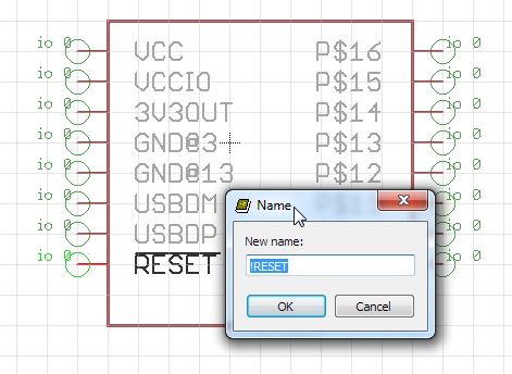
The reset pin is named RESET# which is short hand for 'active low'. Another way to say this is the IC is reset when the pin is pulled low.
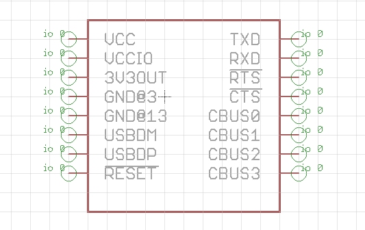
A trick in Eagle: if we put a ‘!’ before the pin name it will put a line over the pin (a line over a pin name is another short hand way to indicate it is active low). This doesn’t have any effect on the overall part or layout, it just looks nice and helps us remember this pin is an active low pin. Do the same for RTS and CTS.
We’ve now got our pins labeled.
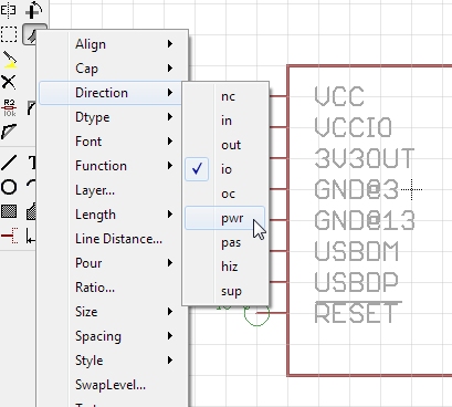
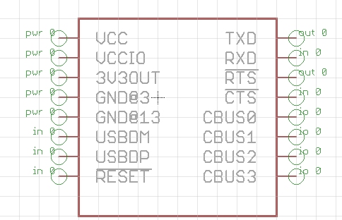
Now we can define each pin type. pwr is good for VCC and GND pins. You can also define inputs and outputs. When in doubt, I leave the pin as the default ‘io’.
Now the pins have direction. These signifiers can help the DRC (design rule check) and ERC (electrical rule check) to detect potential problems with your board. For example, an output is usually not hooked up to another output so the ERC will throw an warning if it detects to output pins connected together.
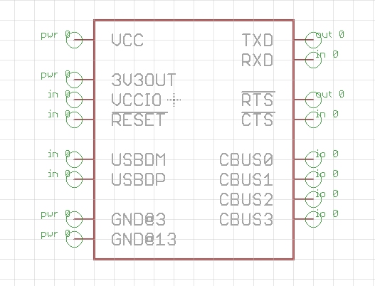
Now hit the F7 button to go into ‘move’ mode. I like to arrange the power and configuration pins on the left side of the symbol and the user accessible pins on the right side.
I chose this configuration for a couple reasons:
- Reset is generally tied high to 3V3OUT so I put them near each other.
- VCCIO can be tied to 3V3OUT or VCC (most commonly 3V3OUT) so it is near VCC and 3V3OUT.
- USBDM is a net that is usually above the USBDP net when connecting it directly to a USB connector. You wouldn’t know this until you lay out a handle of schematics with USB and have to cross the USB+ and USB- nets to get them going into the other component. It’s easier just to put the USBDM pin above the USBDP pin.
- All pins are sort of spread out in groups of what they do. TX and RX and the major pins - top right. Next CTS/RTS get used much less but are often used together. The very neat, but option CBUS pins are off by themselves.
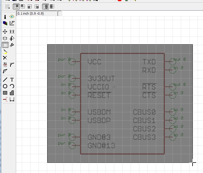
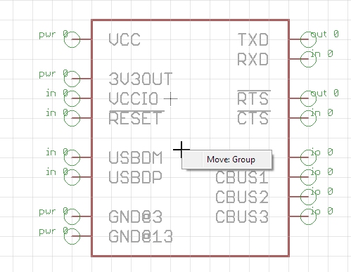
Now let’s center this beast. Hit Alt+F7 to go into ‘group’ mode. Place the cursor in top left corner. Click the mouse and hold, then drag the square to the lower right corner. Release the mouse.
Note how everything is highlighted. You’ve selected all the parts of this schematic symbol.
Now, hold ctrl and right click. You will see the entire group begin to move.
Alternatively (and for you Apple folks without a ctrl key) you can right click then click on the Move:Group menu option. I vastly prefer the ctrl+right click method as it saves you a step.
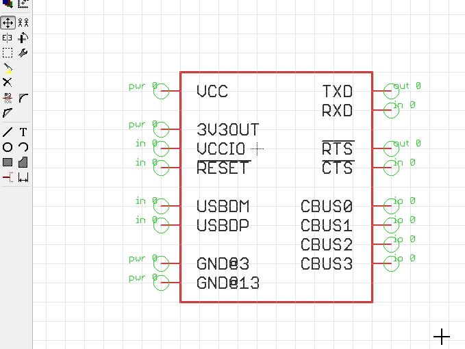
Now move the entire group so that the origin sign (the smaller +) is in the middle of your part. If your part happens to be oblong in one direction, that’s ok, just get it close to the center.
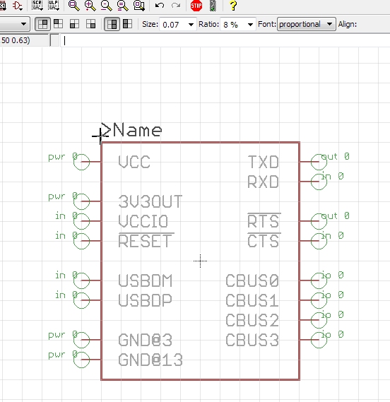
Remember the weird >Name and >Value thing when you created your package? We need to do that again! Click on the ‘text’ button. Type ‘>Name’ and press enter. Before placing the text, click your scroll wheel and goto the >Names layer.
I did a couple things before left clicking the mouse and dropping the text into place:
- Increased the text size to 0.07
- Held alt while moving my text so that it is not right up against the border of our part. Makes it easier to read when we create PDFs and print schematics.
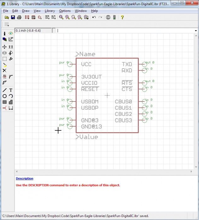
Repeat for >Value. Save your work!
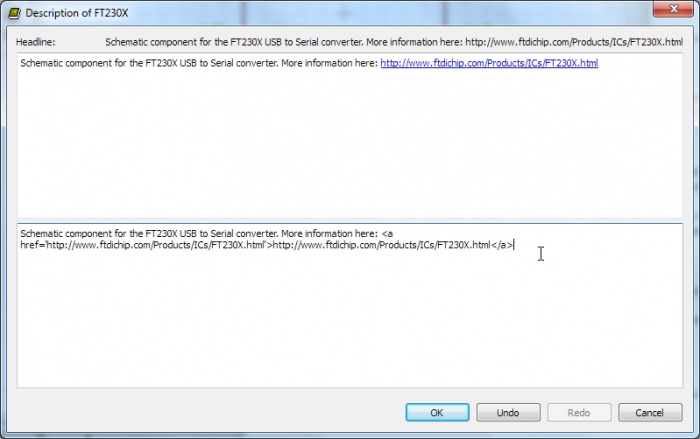
Be sure to add a description to your part. Check it out! We can add some basic HTML markup if we want!
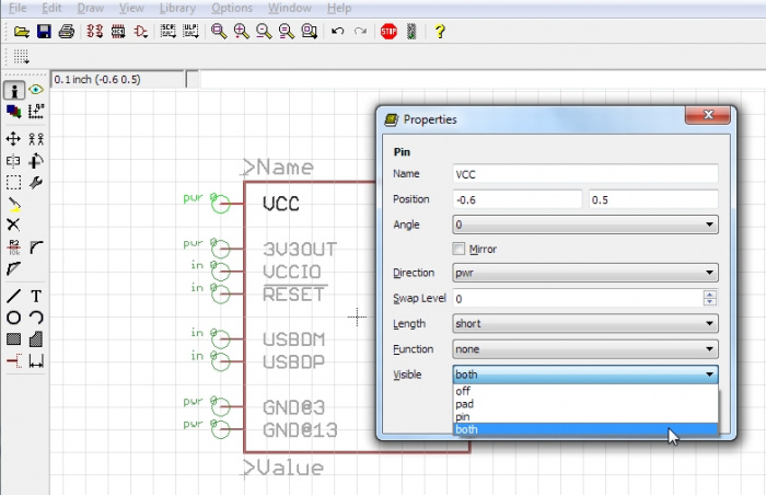
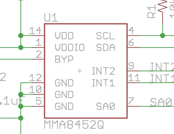
Click on the 'i' then on a given pin. By default, every pin has the ‘Visible’ option set to ‘both’. This means both the number assigned to this pin and the pad fuction will be displayed. This will show on your schematic like this:
It depends on the part, but I often think showing the pin numbers is more information than is needed and begins to make the part look cluttered. For example, we don’t need to know that the BYP pin on this device is also pad 2 on the IC footprint, we just need to know that this connection point is for the bypass cap.
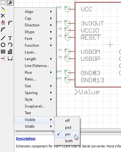
To turn this off, we set the ‘Visible’ option to ‘pin’ on each pin.
Click on the ‘change’ wrench, Visible, then pin. Then click on each pin. You won’t see anything change on the schematic component but it will be reflected on your overall schematic.
Hit save and you’re done! Next we move on to Device creation.
Device Creation
Eagle requires three things to get an IC into the library:
- Package (also known as a footprint)
- Symbol (the schematic symbol)
- Device (mapping them together)
The tutorial images show us working from the SparkFun-DigitalIC.lbr file but you can create your own custom library file if you'd like.
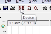
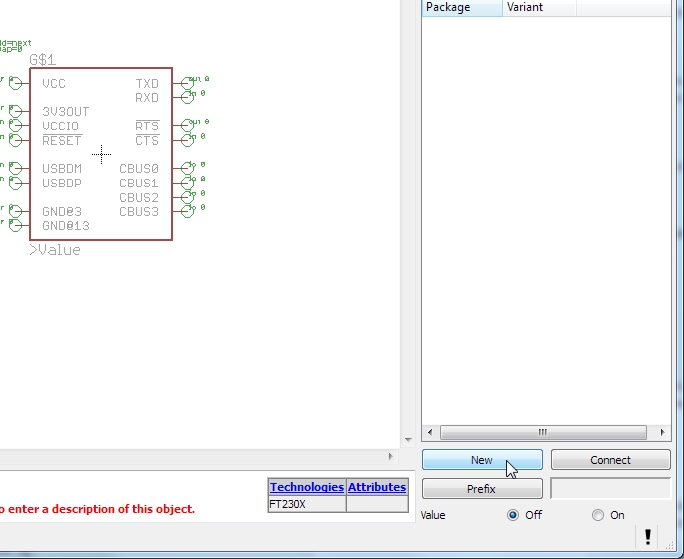
It’s time to create a device. The device maps the make-believe schematic symbol to the real-world footprint. Start by clicking on the device button.
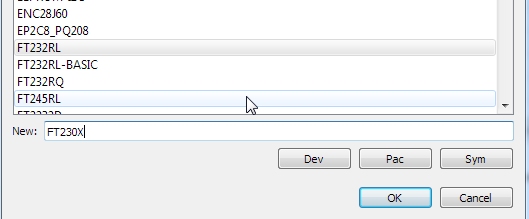
It’s always good practice to check to see if we already have a device created. From the device list you can see that we do not currently have anything like the FT230X device, so let’s create a new one.
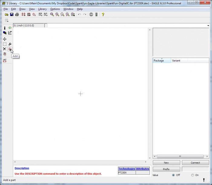
First step, click on ‘add’ to add the schematic symbol to your device. Navigate the list of symbols until you find the ‘FT230X’ you created earlier. Double click it.
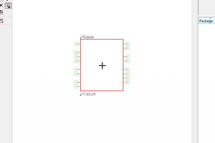
Drop your symbol so that the center of the symbol aligns with the center of the device space and left click your mouse. Hit escape twice to exit back to the main window.
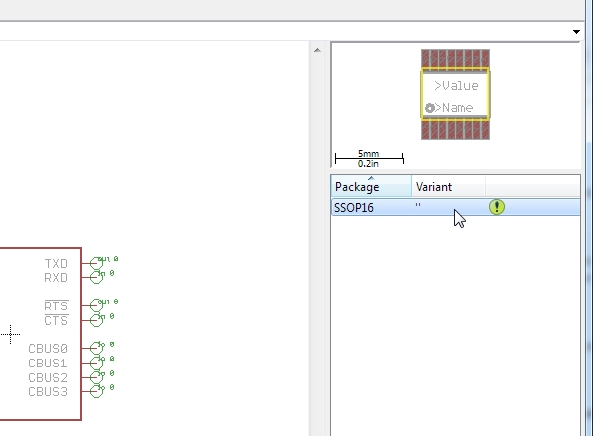
Now click on ‘New’ package. Navigate to the SSOP16 package you created earlier and double click.
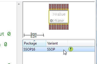
In the main window you’ll see a new package with variant labeled “ (this is the default) and an exclamation point.
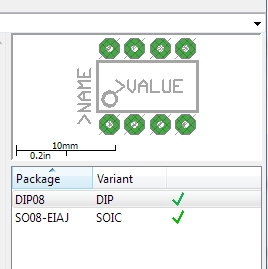
A given integrated circuit may be pacakged in a varienty of different shapes and sizes (for example DIP, SSOP, or smaller QFN type packages). The variant name allows you to have multiple footprints for the same schematic symbol.
The ATtiny shown above is a good example. The IC is the same but it comes in two different footprints: 8 pin DIP and 8 pin SOIC. You cannot have a duplicate variant name so in this example we used 'DIP' and 'SOIC'.
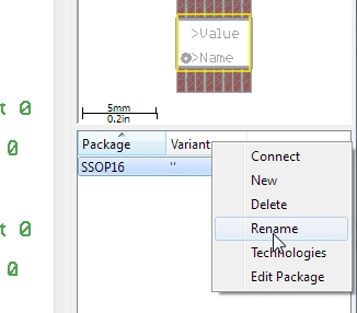
Eagle will not allow you to have two packages with the same variant name. To change the variant name, right click on the package type and click ‘Rename’. Give this package a name such as SMD or DIP or SSOP. Whatever you need to make it clear what package variant this is.
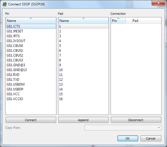
Next we need to tell Eagle what pad on the package goes with which pin on the symbol. Double click the bar under the package window, or click on the button ‘Connect’ at the bottom of the window.
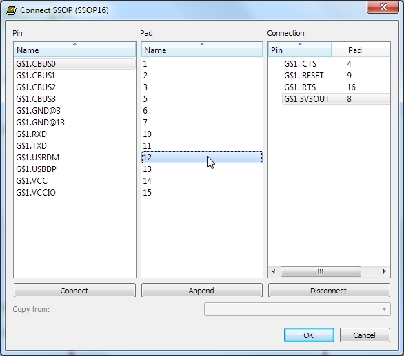
This is a very important step. We must refer to the datasheet for the FT230X and be very careful to correctly connect the pins and pads correctly. CTS is pad 4 so with CTS highlighted, double click on 4 in the pad list.
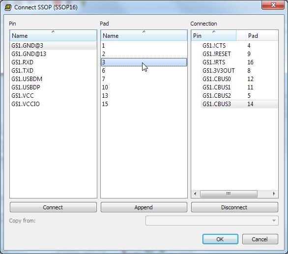
Continue until you’ve connected all the pins to the pads. If you have pins left over, that’s bad and Eagle will complain. However, if you have pads left over, that’s ok - you probably have some pads on the footprint that are left unconnected.
If you do have anything left over, this is a good time to double check that you’ve correctly identified all the pads and pins on your footprint and schematic symbol correctly.
Remember when we named the pins GND@3 and GND@13? Guess which pad GND@3 connects to? Pad 3! And GND@13? Pad 13! This is why we used that @ sign - to make it easier when we have multiple pins of the same name to connect to different pads.
Once you’re done you should have a nice green check mark next to your variant.
Note the G$1 over the symbol. The ‘G’ is wrong for integrated circuits (we normally use ‘U’) and the ‘$’ is super annoying and looks bad on the schematic. To get rid of this, click on the ‘Prefix’ button in the lower right corner and type ‘U’ with nothing else. This will make the default prefix ‘U’ instead of G$. Upon returning to the main window the G$1 will still be there. To change that, press F4 and click on the symbol. You can then change the name to U1.
Be sure to give a good, lengthy description of your device! It will help tremendously when you have a library of 100 different parts. Now save your work!
Resources and Going Further
That’s it! I hope you’ve enjoyed reading this tutorial about how to make a new footprint, schematic symbol and device under Eagle. From here, you should use the device on a PCB!
To learn more, we recommend you checkout the following:
- Connector Basics
- How to layout an SMD PCB
- SMD Soldering
- Steciling and Reflow
- Creating Custom Footprints in Eagle
- Electronics Assembly
If you'd like to share your PCB creations with the world, check out these tutorials:
